行政院國家科學委員會專題研究計畫 成果報告
研發具有高穩定性的主動驅動有機電激發光顯示器之驅動 電路
計畫類別: 個別型計畫
計畫編號: NSC93-2215-E-011-005-
執行期間: 93 年 08 月 01 日至 94 年 07 月 31 日 執行單位: 國立臺灣科技大學電子工程系
計畫主持人: 范慶麟
計畫參與人員: 張志榜
報告類型: 精簡報告
處理方式: 本計畫涉及專利或其他智慧財產權,2 年後可公開查詢
中 華 民 國 94 年 10 月 25 日
I
中文摘要
在本專題計畫的研究中,我們成功證明以準分子雷射(ELA)結晶之複晶矽薄膜電晶體 (poly-Si TFTs)在主動式有機發光顯示器(AMOLEDs)之可用性。研究中所設計之 AMOLEDs 面
板大小為1.9 吋、解析度為 160 x 120 x 3,畫素驅動是由兩顆驅動電晶體與一個儲存電容(2T1C)
所組成,並透過 H-SPICE 模擬軟體針對設計之驅動電路與 AMOLEDs 之亮度均勻性進行模
擬,電路模擬之TFTs 參數採用 RPI poly-Si TFT model 並套用實際製作之 ELA poly-Si TFTs 的
各項特性與參數。由模擬結果顯示,儲存電容之充放電時間為41 μsec,較掃描時間(50 μsec)
短,則TFT2 之輸出電流足夠驅動 AMOLEDs 面板。此外,本研究所設計之 TFT 之漏電流相
當小,當 TFT1 切換至 off 狀態時,對儲存電容之電壓影響不大,因此可獲得一亮度均勻之
AMOLEDs 面板。
關鍵字:準分子雷射、低溫多晶矽、有機發光二極體、主動式
Abstract
We demonstrate the practicability of the ELA poly-Si TFTs fabricated in this project. The devices had been investigated and they were used as active elements in the pixel circuit for a simulation design of a 1.9-inch active-matrix organic light emitting diode displays (AMOLEDs) with a resolution of 120 x 160 x 3 using an H-SPICE circuit simulator. The circuit parameters of the poly-Si TFTs are extracted using the RPI poly-Si TFT model. The main concerning issue of the AMOLEDs pixel design is the uniform brightness throughout the display, and the preferred design approach is the two TFTs per pixel structure in conjunction with a good process control. The results of simulation indicate that the ELA poly-Si TFTs are capable of acting as active elements in the AMOLEDs application.
Keywords: ELA, LTPS TFT, OLED, AMOLED
I. Introduction
A variety of technologies are competing for a share of the flat panel displays (FPDs) market.
Active Matrix Liquid-crystal display (AMLCD) is presently the dominant FPD technology because of its portability and mature manufacturing practice. However, LCD technology has some problems, such as power efficiency and limited viewing angle [1]. Therefore, alternative flat panel technologies will be able to complete. A new emissive technology, kown as organic light emitting diode displays (OLEDs), has been intensely studied since Tang [2] demonstrated efficient electroluminescence (EL) from a bi-layer device. In addition to sharing many of the favorable attributes with liquid crystals, OLEDs are attractive as alternative display elements because of their relative merits of being self-emitting, having large intrinsic viewing angle and fast switching speed.
Thus, many companies have focused their research to develop passive-matrix (PM) [3] and active matrix (AM) driving [4-5] schemes for the OLEDs applications. The AM driving method is better for high-resolution display as the pixels may be driven close to their best power efficiency point.
In this project, we will first extract the parameter of poly-Si TFTs’ Spice-model, and then discuss the concerning issues and design approach of AMOLED pixel circuits. Finally, the design of the 1.9-inch AMOLED with a resolution of 120 x 160 x 3 is demonstrated with H-spice circuit simulator including the extracted circuit parameter of poly-Si TFT.
II. Description and Parameter extraction of poly-Si TFTs’ Spice-model
A semi-empirical analytical model, named as RPI poly-Si model, for the DC characteristics of both n- and p-channel poly-Si TFTs had been developed by Michael S. Shur [6-8]. The models should be physically based so that they employ a minimum of parameters which can be extracted on a routine basis in a manufacturing environment. Thus, the model is suitable for implementation in a H-spice circuit simulator. The RPI poly-Si TFT model describes all four regions of operation including leakage, subthreshold, above threshold, and kink regions.
However, to facilitate quick convergence in SPICE simulator, the models for all regions of operation should be combined into a single expression which is everywhere continuous and smooth.
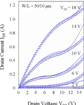
This is accomplished by defining effective voltages which cause the models to become insignificant outside of their regions of applicability. Comparison of the model versus measured data is shown in Fig. 1 and Fig. 2 for n-channel LTP ELA poly-Si TFTs with a dimension of W/L = 50/10 μm. The performance of the modeled poly-Si TFT is improved with fluorine ion implantation. Bases on the mechanism of the RPI poly-Si TFT model, it can be found that the modeling data is quite agreement with the measurements except the deviation of the kink region.
III. Concerning issues and design approach
OLED displays have been designed in both passive matrix and active matrix modes. Within AMOLED designs, a variety of pixel architectures have been proposed [9-12]. Different pixel architectures may contain different number of transistors per pixel. The simplest design uses one transistor per pixel. The design will have a higher yield than designs containing more than 1 TFT per pixel. Each pixel will only emit light for a fraction of the frame period as a result of the lack of
the pixel memory. This requires the peak OLED current to be much higher than the average current corresponding to the average luminance, which leads to faster degradation of the OLED material.
Fig. 3 shows a schematic of the pixel for this approach. To avoid the high current pulses native to the single TFT design, designs involving two transistors per pixel have been proposed, which have the effect of pixel memory [9]. One transistor is used to set a voltage on the gate of a second transistor. The second TFT will deliver a continuous current through the OLED material throughout the entire frame time, as shown in Fig. 4. This design method has the advantages of reduced drive current and thus improved OLED material lifetime compared with the single TFT per pixel approach. The fundamental problem of this pixel circuit is that the variation of characteristics of driving transistor throughout the display area directly corresponds to the pixel-to-pixel brightness non-uniformity.
The OLED brightness is directed related to the current flow through the device as a result of the nature of the light emission process. Thus, it is critical to achieve a constant current flow in the OLED in order to control the FPD brightness uniformity. Therefore, various processing issues regarding the uniformity of device performances will arise for the development of AMOLEDs.
Besides the improvement of process uniformity can lead to the uniform brightness, p-channel poly-Si TFTs are desired to prevent variations in the OLED material turn-on voltage from leading to current variations in the OLED material. In addition, recent work has demonstrated further advantages to place even more transistors (≧3 transistors per pixel) at each pixel, such as improved brightness uniformity by correcting for variations in the transistor electrical characteristics [10-12].
However, the more complicated pixel circuits for the compensation of transistor electrical characteristics usually result in the decreasing of the yield rate. In the mass-production, the trade-off
Fig. 1 Comparison of measured (markers) and modeled(curves) drain current (IDS) vs. gate voltage (VGS) for n-channel fluorine ion implanted ELA Poly-Si TFT.
Fig. 2 Comparison of measured (markers) and modeled (curves) drain current (IDS) vs. drain voltage (VDS) for n-channel fluorine ion implanted ELA Poly-Si TFT.
between the yield rate and the complication of pixel circuits must be considered simultaneously.
Thus, the improved process uniformity and p-channel active elements are the superior candidate than that of the complicated pixel circuits for the purpose of uniform brightness throughout the small size AMOLEDs.
Fig. 3 Schematics of the pixel circuits showing the single TFT per pixel design for active matrix organic light-emitting diode displays.
Fig. 4 Schematics of the pixel circuits showing the two TFTs per pixel design for active matrix organic light emitting diode displays. A pixel is composed of a switching TFT (TFT1), a driving TFT (TFT2), a storage capacitor (Cs), and an organic light-emitting diode (OLED).
IV. Simulation design of 1.9-inch AMOLEDs with a resolution of 120 x 160 x 3
The circuit schematic of the pixel of 1.9 inches AMOLED with a resolution of 120 x 160 x 3 is shown in Fig. 5. The pixel comprises two TFTs, a storage capacitor and a light emitting OLED, which were arranged on a glass substrate. The gate electrode of TFT1 comprises a portion of a gate bus (scan line). The source electrode of TFT1 is electrically connected to a source bus (data line).The gate electrode of TFT2 is electrically connected to the drain electrode of the TFT1. A storage capacitor is charged from an excitation signal source through TFT1, and discharges during the dwell time to provide nearly constant potential to the gate electrode of TFT2. An anode layer is electrically connected to the source electrode of TFT2 and the cathode layer is connected to ground node. The power source driving all pixels is electrically to the drain electrode of the TFT2. The structure is conventional for current consuming devices. However, there are some disadvantages, for example, nonuniformity caused by variation of the characteristics for the driving TFT. We chose the structure because the simplicity is very practical when we avoid the yield rate problem in mass production.
In this circuit, the OLED is represented by a TFT (TFT3) in combination with a diode capacitance (Cdiode) in parallel. The TFT3 and Cdiode were optimized to ensure that under the forward bias condition the current flow in TFT3- Cdiode combination is similar to the one expected for the OLEDs. This circuit has four external terminals including power line (VDD), ground (GND;
OLED cathode), data line (Vdata), and scan line (Vscan). Vscan is the scan line signal and Vdata is data voltage signal. VDD and GND terminals are common power sources connected to all pixels on the panel. The operation of this circuit can be described as follows. In the ON state, when the scan line (Vscan) is high, TFT1 is turned ON. The data line signal (Vdata) then passes through TFT1 and sets the gate voltage of TFT2 and the voltage level of the storage capacitor (Cs). Consequently, the TFT2 will be turned ON as a result of the setting of gate voltage of TFT2 to allow the current flowing from VDD through TFT2 into OLED to ground. In the OFF state, when the pixel circuit is deselected and the select signal is low, the TFT1 is OFF. The TFT2 gate voltage is maintained at the previous level by the charges stored in the storage capacitor Cs. Consequently, the output current (IOUT) is maintained at the same level as that in the ON state. Thus, the continuous emitting-light of the OLED is conducted with a very low peak driving current.
Fig. 5 The pixel electrode circuit using two TFTs for 1.9-inch AMOLEDs with a resolution of 120x160x3.
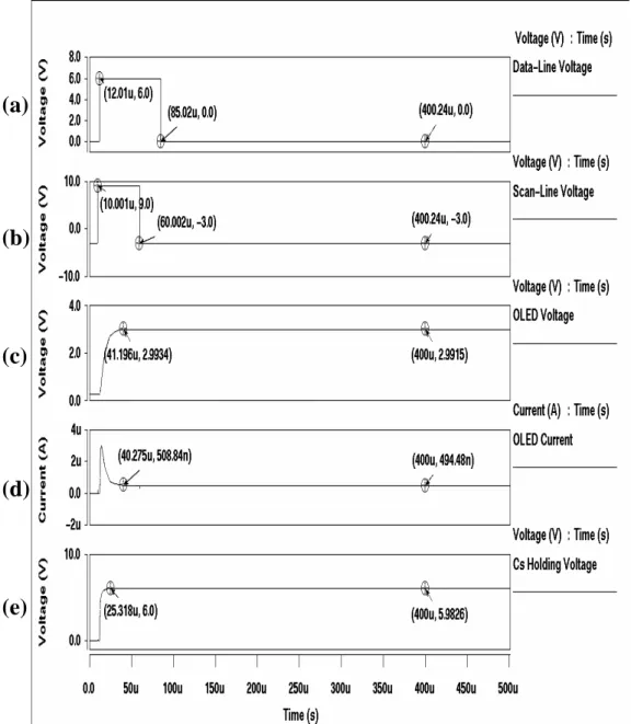
To support the circuit analysis, pixel electrode circuit simulation has been performed on a SUN solaris-8 work-station using H-spice circuit simulator including RPI poly-Si TFT model. The circuit parameter of the ELA poly-Si TFTs that were fabricated using fluorine ion implantation to improve performance has been extracted and included into H-spice circuit simulator. The pixel electrode circuit simulation parameters are tabulated in Table 1. Fig. 6(a)-(b) and Fig. 6(c)-(e) show the input signal and simulation results of the pixel electrode circuit, respectively. The frame rate of the 1.9-inch AMOLEDs with a resolution of 120 x 160 x 3 is 60 Hz. The voltage level of input data is 6 V with a pulse width of 73 μsec, as shown in Fig. 6(a). The input scan voltage level is set from –3 to 9 V with a pulse width of 50μsec, as shown in Fig. 6(b). When the pixel electrode circuit is selected, i.e., Vscan = 9 V, signal data voltage (Vdata) is fed through switch transistor (TFT1) to the gate of drive transistor (TFT2). TFT2 controls the current flowing into OLED in accordance to the fed gate voltage. The Fig. 6(c)-(d) illustrate the simulated voltage and current across OLED. The results indicate that the TFT2 can provide a driving current of 0.5 μA into OLED as well as a corresponding voltage of 3 V across OLED throughout all frame time. In addition, we can also find that the charging time (41 μsec) of Cdiode is smaller than the selecting time of the scan line (50 μsec), which can prove that the on-current of TFT1 is enough to drive the AMOLEDs. Fig. 6(e) shows the transient analysis of the voltage level of storage capacitor. We can find that the decrease of the voltage level of storage capacitor is very small after the TFT1 switching-off as a result of the TFT1s’ low leakage current. Thus, the holding voltage of storage capacitor will enable the pixel to continue providing the almost same current as that in the ON state after the addressing period, as shown in Fig. 6(c). It is to say that the simulation design indicates that the pixel can continue emitting the same light intensity in the ON and OFF state, which is the requirement of the product of 1.9-inch AMOLEDs with a resolution of 120 x 160 x 3.
Table 1 Pixel electrode circuit simulation parameters
VDD (V) Vscan (V) Vdata (V)
μFE (cm2/V.sec) Vth (V)
W1/L1 (μm) W2/L2 (μm) W3/L3 (μm) Cs (pF) Cdiode (PF)
6 -3Æ9 6 70 2.5 4/10 20/10 20/10 0.5 8
Fig. 6 Input signals and transient simulation results for the pixel electrode circuit using two TFTs structure: (a) input data signal, (b) input scan signal, (c) voltage across OLED, (d) current flowing through OLED, and (e) Cs holding voltage.
V. Conclusion
In this project, the ELA poly-Si TFTs has been applied to 1.9-inch AMOLEDs with a resolution of 120 x 160 x 3 as the active elements. The circuit parameters of the poly-Si TFTs are extracted by RPI poly-Si model and are then included into the Hspice circuit simulator. The RPI poly-Si model can be divided into four operation regions for ELA poly-Si TFTs electrical characteristics, including leakage, subthreshold, above threshold, and kink region. The dominate mechanisms in each region are described and the modeling data is quite agreement with the measurements except the deviation of the kink region. The concerning issues of AMOLEDs pixel design mainly is the uniform brightness throughout the display and the preferred design approach is the two TFTs pixel structure with the lowest process variation. Finally, the application of ELA poly-Si TFTs to AMOLEDs with
(a)
(b)
(c)
(d)
(e)
a resolution 120 x 160 x 3 is performed with Hspice circuit simulator. From the simulation results, we can find that the charging time (41 μsec) of Cdiode is smaller than the selecting time of the scan line (50 μsec), which can prove that the on-current of TFT1 is enough to drive the AMOLEDs. We can also find that the decrease of the voltage level of storage capacitor is very small after the TFT1 switching-off as a result of the TFTs’ low leakage current.
VI. 研究成果自評
在本專題計畫的研究中,我們成功證明以準分子雷射(ELA)結晶之複晶矽薄膜電晶體 (poly-Si TFTs)在主動式有機發光顯示器(AMOLEDs)之可用性。研究中所設計之 AMOLEDs 面
板大小為1.9 吋、解析度為 160 x 120 x 3,畫素驅動是由兩顆驅動電晶體與一個儲存電容(2T1C)
所組成,並透過 H-SPICE 模擬軟體針對設計之驅動電路與 AMOLEDs 之亮度均勻性進行模
擬,電路模擬之TFTs 參數採用 RPI poly-Si TFT model 並套用實際製作之 ELA poly-Si TFTs 的
各項特性與參數。由模擬結果顯示,儲存電容之充放電時間為41 μsec,較掃描時間(50 μsec)
短,則TFT2 之輸出電流足夠驅動 AMOLEDs 面板。此外,本研究所設計之 TFT 之漏電流相
當小,當 TFT1 切換至 off 狀態時,對儲存電容之電壓影響不大,因此可獲得一亮度均勻之
AMOLEDs 面板。綜上所述,此計劃之研究成果除可使執行計畫之學生獲得 AMOLEDs 之模 擬設計能力外,對於工業界之實際應用亦有相當的價值。
References
[1] W. Goede, SID Seminar Notes, (1995) M-0.
[2] C. W. Tang and S. A. Vanslyke, Appl. Phys. Lett., 51, 913 (1987).
[3] E.I. Haskal, M. Buechel, A. Sempel, S. K. Heeks, J. C. Carter, W. Wu, J. O’Brien, M. Fleuster,
and R. J. Visser, Proceeding of Asia Display’01, (2001), p. 1411.
[4] Y. He, R. Hattori, and J. Kanicki, IEEE Electron Device Lett., EDL-21, 590 (2000).
[5] M. Stewart, Robert S. Howell, Leo Pires, and Miltiadis K. Hatails, IEEE Trans. Electron
Devices, ED-48, 845 (2001).
[6] Y. Byun, M. Shur, and M. Hack, in Proc. 1991 ISDRS, p.537.
[7] M. Shur, M. Hack, and Y. Byun, in Proc. 1993 ISDRS, p. 165.
[8] M. Jacunski, M. Shur, and M. Hack, IEEE Trans. Electron Devices, ED-43, 1433 (1996).
[9] M. K. Hatails, M. Stewart, C. W. Tang, and J. Burtis, Proc SPIE, 3057, 277 (1997).
[10] Y. He, R. Hattori, and J. Kanicki, IEEE Electron Device Lett., EDL-21, 590 (2000).
[11] R. Dawson, Z. Shen, D. A. Furest, and S. Conner, in Symp. Dig. 1998 SID, p.11.
[12] T. Sasaoka, M. Sekiya, A. Yumoto, and J. Yamada, in Symp. Dig. 2001 SID, p.384.