Deposition of SiO
2Layers on GaN by Photochemical
Vapor Deposition
Shoou-Jinn Chang,a,zYan-Kuin Su,aYu-Zung Chiou,aJung-Ran Chiou,b
Bohr-Ran Huang,bChia-Sheng Chang,aand Jone F. Chena
aInstitute of Microelectronics and Department of Electrical Engineering, National Cheng Kung University, Tainan, Taiwan 70101
b
Institute of Electronics and Information Engineering and Department of Electronic Engineering, National Yunlin University of Science and Technology, Touliu, Taiwan 640
SiO2 insulating layers were first deposited onto GaN by photochemical vapor deposition共photo-CVD兲 technology using a deuterium (D2) lamp as the excitation source. Physical, chemical, and electrical characteristics of the Al/SiO2/GaN metal-insulator-semiconductor共MIS兲 capacitors are reported for the first time. It was also found that the limiting factor of SiO2growth rate was the number of SiH4 and O2 molecules available to provide excited Si and O atoms. Furthermore, it was found from high-frequency capacitance-voltage measurements that the photo-CVD SiO2/n-GaN interface state density, Dit, was estimated to be 8.4⫻ 1011cm⫺2eV⫺1for the photo-CVD SiO
2layers prepared at 300°C. With an applied field of 4 MV/cm, the oxide leakage current density was found to be only 6.6⫻ 10⫺7A/cm2.
© 2003 The Electrochemical Society. 关DOI: 10.1149/1.1534598兴 All rights reserved.
Manuscript submitted February 26, 2002; revised manuscript received May 20, 2002. Available electronically January 6, 2003.
The excellent physical and electrical properties of GaN have made it a good candidate in temperature, power, and high-frequency applications.1 High quality III-V ternaries such as AlxGa1⫺xN and InyGa1⫺yN were also demonstrated for heterojunc-tion field effect transistors 共HFETs兲,2,3 bipolar junction transistors
共BJTs兲,4and light-emitting diodes共LEDs兲.5Nitride-based blue and green LEDs6are already commercially available. The high disloca-tion density measured in these blue/green LEDs has led to the con-clusion that dislocations in group III nitrides are not efficient recom-bination centers. Such a dislocation density also suggested that the number of surface states is small in GaN.7,8 Recently, many re-searches were focused on the fabrication of GaN-based metal-insulator-semiconductor共MIS兲 capacitors with SiO2,9,10Si3N4, and Ga2O311,12as the insulating material. It has been reported that SiO2 layers can be deposited onto GaN by plasma-enhanced chemical vapor deposition9,10and liquid-phase deposition.13Previously, it was shown that photochemical vapor deposition共photo-CVD兲 can also be used to grow high quality SiO2 layers14-18on various semicon-ductor substrates. In using photo-CVD to grow thin films, selecting the proper light source with a radiation spectrum matching the ab-sorption spectra of the reactance gases is very important. In this study, we used a deuterium (D2) lamp as the excitation source. It is known that D2lamp emits strong ultraviolet共UV兲 and vacuum ul-traviolet 共VUV兲, which can effectively decompose SiH4 and O2, since O2could absorb photons in the wavelength region from 133 to 175 nm and SiH4 could absorb photons in the wavelength region below 147 nm.14-18Thus, energy can be directly transferred from the D2lamp to the excited Si and O atoms. In addition, such a photo-CVD system offers better control in the oxide region and selective growth is possible. The quality of oxide layers grown by such a photo-CVD system is close to that grown by thermal oxidation, and the electrical properties of the photo-CVD grown oxide are accept-able for device applications.14-18 In this paper, the deposition of SiO2 layers on GaN and the properties of Al/photo-CVD SiO2/n-GaN MIS capacitors are reported for the first time.
Experimental
Prior to the deposition of SiO2layers, an n-type GaN epitaxial layer was grown on 共0001兲 sapphire substrates by metallorganic chemical vapor deposition共MOCVD兲.19-34The electron concentra-tion of the n-type GaN epitaxial layer was about 5⫻ 1017cm⫺3.
The 50 nm thick SiO2films were subsequently deposited onto the GaN epitaxial layer by 150 W D2lamp photo-CVD under different process pressures and different substrate temperatures. The gas ratio was fixed at SiH4/O2⫽ 0.055.10-14 For comparison, SiO2 films with the same thickness were also deposited on the same GaN epi-taxial layer by rf magnetron sputtering. Atomic force microscopy
共AFM兲 and Auger electron spectroscopy 共AES兲 were then used to
characterize the deposited SiO2films. Al/SiO2/GaN MIS capacitors were subsequently prepared by etching and metal evaporation. The capacitance-voltage共C-V兲 and current-voltage (I-V) characteristics of these fabricated MIS capacitors were then measured by an HP 4284B LCR meter and an HP 4156B semiconductor parameter ana-lyzer, respectively.
Results and Discussion
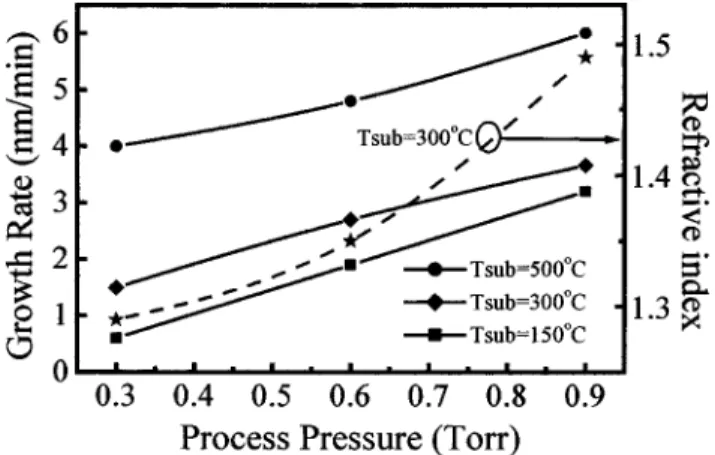
Figure 1 shows SiO2growth rate as a function of process pres-sure for the photo-CVD SiO2 layers grown at different substrate temperatures. It was found that the SiO2growth rate increases as the substrate temperature increases. It was also found that the SiO2 growth rate increases linearly as the process pressure increases. Such a linear increase suggests that the limiting factor for growth rate is the amount of SiH4and O2 molecules available to provide excited Si and O atoms. At higher process pressure, the number of
zE-mail: [email protected]
Figure 1. SiO2 growth rate as a function of process pressure for samples grown at different substrate temperatures. The refractive index of the 300°C grown SiO2layer is also shown.
Journal of The Electrochemical Society, 150共2兲 C77-C80 共2003兲
0013-4651/2003/150共2兲/C77/4/$7.00 © The Electrochemical Society, Inc.
C77
excited Si and O atoms will increase so as to result in a higher SiO2 growth rate. The refractive index of the 300°C photo-CVD grown SiO2 layer prepared at different process pressure is also shown in Fig. 1. It can be seen that the refractive index also increases as the process pressure increases. Such an observation is probably due to the fact that the SiO2layer prepared at high process pressure is more
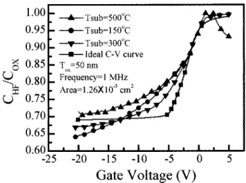
condensed again due to the increased number of excited Si and O atoms. It should be noted that the refractive index of the 300°C photo-CVD grown SiO2 layer prepared at 0.9 Torr is very close to that of the thermally grown SiO2 layer prepared on top of Si sub-strates. Figures 2a, b, and c show the AFM images of bare GaN without SiO2, photo-CVD SiO2 grown at 300°C and sputtered SiO2, respectively. It was found that the root mean square 共rms兲 roughness was 1.85, 2.8, and 1.3 nm for bare GaN without SiO2, photo-CVD SiO2grown at 300°C, and sputtered SiO2, respectively. The smooth surface observed from the sputtered SiO2was probably due to its amorphous nature. Figures 3a and b show the AES depth profiles of sputtered SiO2 and photo-CVD SiO2 grown at 300°C, respectively. It could be seen from Fig. 3b that the depth profile was uniform in the insulating layer with an O/Si ratio almost equal to 2 for the photo-CVD SiO2grown at 300°C. In contrast, although the depth profile was also uniform in the insulating layer for the sput-tered SiO2, its O/Si ratio was only 1.5. Such a result suggests that the composition of the sputtered insulating layer is SiO1.5, instead of SiO2. Such a result also suggests that there exist a large number of dangling bounds in the sputtered SiO2due to the lack of oxygen. Figure 4 shows the C-V characteristics共1 MHz兲 of the photo-CVD SiO2 grown at different temperatures. The ideal C-V curve
Figure 2. AFM images of SiO2films prepared by photo-CVD and sputter.
Figure 3. AES spectra of SiO2films prepared by photo-CVD and sputtering.
Figure 4. High frequency 共1 MHz兲 C-V characteristics of Al/SiO2/GaN MIS capacitors.
Journal of The Electrochemical Society, 150共2兲 C77-C80 共2003兲 C78
was also plotted in the same figure. It was found that no significant hysteresis was observed as the gate voltage varied at 0.1 V/s from
⫹5 V to ⫺20 V and then back to ⫹5 V for all three samples. The
lack of hysteresis in these C-V curves indicated that the number of mobile ions in SiO2 layer is negligibly small. At high frequency measurement共1 MHz兲, there is not enough response time for minor-ity carriers 共holes for n-GaN兲 to be generated in n-GaN, so that significant inversion characteristics could not be observed from this figure. Similar results were also observed by Casey et al.13Using the standard high frequency capacitance method,35we can thus cal-culate the interface state density from these C-V curves
Dit⫽ Cox q
冋
冉
d⌿s dVg冊
⫺1 ⫺ 1册
⫺ Cs q 关1兴where Coxand Cswere the oxide and depletion capacitance, respec-tively,⌿swas the band bending, and Vgwas the gate voltage. From Eq. 1, it was found that Dit equals 1.2⫻ 1012 and 8.4
⫻ 1011
cm⫺2eV⫺1for photo-CVD SiO2layers on GaN prepared at 150 and 300°C, respectively. The smaller Dit for the photo-CVD SiO2layer deposited at 300°C could be attributed to the fact that a higher substrate temperature can significantly improve the SiO2/GaN interfacial properties probably through supplying ther-mal energy to the Si and O atoms. Compared to Ga2O3 on GaN reported by Fu et al., the Ditof our photo-CVD SiO2 prepared at 300°C on GaN was one order of magnitude smaller. The Dit ob-served from our photo-CVD SiO2/n-GaN interface was also com-parable to those observed from PECVD SiO2/n-GaN interfaces re-ported by Arulkumaran et al.10However, Ditwas increased to 6.4
⫻ 1012
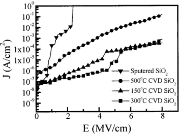
cm⫺2eV⫺1 when the substrate temperature was increased to 500°C. The exact reason for the increase in Ditis not clear yet. Possible reasons for such degradation in oxide quality include too fast an oxide growth rate and/or some interface reactions, which occur at high temperatures. Figure 5 shows the I-V characteristics of the four fabricated Al/photo-CVD SiO2/n-GaN MIS capacitors. During I-V measurement, all capacitors were biased in accumula-tion. It was found that the leakage currents of the photo-CVD grown SiO2layers were all much smaller than that of the sputtered SiO2 layer. This could be understood by the poor quality of the sputtered SiO2layer. Furthermore, it was found that photo-CVD SiO2 depos-ited at 300°C exhibits the smallest leakage current among the four samples. Such a result also agrees well with the C-V data shown in Fig. 4. With an applied field of 4 MV/cm, it was found that the leakage current was only 6.6⫻ 10⫺7 A/cm2 for the photo-CVD SiO2layer deposited at 300°C, as shown in Fig. 5.
Conclusions
In summary, Al/photo-CVD SiO2/n-GaN MIS structures were fabricated by photo-CVD technique using a deuterium (D2) lamp as the excitation source. It was found that the limiting factor for the SiO2growth rate is the number of SiH4and O2molecules available to provide excited Si and O atoms. It was also found that we could achieve a low interface state density, of 8.4⫻ 1011cm⫺2 eV⫺1. Furthermore, it was found that the leakage current was only 6.6
⫻ 10⫺7 A/cm2 with an applied field of 4 MV/cm for the 300°C photo-CVD grown Al/SiO2/GaN MIS capacitor.
Acknowledgments
The authors acknowledge the financial support from the National Science Council for their research grant of NSC 90-2215-E-008-043 and NSC 90-2112-M-008-046.
National Cheng Kung University assisted in meeting the publication costs of this article.
References
1. T. Tojyo, T. Asano, M. Takeya, T. Hino, S. Kijima, S. Goto, S. Uchida, and M. Ikeda, Jpn. J. Appl. Phys., Part 1, 40, 3206共2001兲.
2. J. B. Webb, H. Tang, J. A. Bardwell, and P. Coleridge, Appl. Phys. Lett., 78, 3845
共2001兲.
3. A. Tarakji, G. Simin, N. Ilinskaya, X. Hu, A. Kumar, A. Koudymov, J. Yang, M. Asif Khan, M. S. Shur, and R. Gaska, Appl. Phys. Lett., 78, 2169共2001兲. 4. S. Yoshida and J. Suzuki, Jpn. J. Appl. Phys., Part 2, 38, L851共1999兲. 5. S. Nakamura, T. Mukai, and M. Senoh, J. Appl. Phys., 76, 81989共1994兲. 6. T. Mukai, M. Yamada, and S. Nakamura, Jpn. J. Appl. Phys., Part 1, 38, 3976
共1999兲.
7. S. D. Lester, F. A. Ponce, M. G. Craford, and D. A. Steigerwald, Appl. Phys. Lett., 66, 1249共1995兲.
8. Y. K. Su, Y. Z. Chiou, F. S. Juang, S. J. Chang, and J. K. She, Jpn. J. Appl. Phys.,
Part 1, 40, 2996共2001兲.
9. H. C. Casey, Jr., G. G. Fountain, R. G. Alley, B. P. Keller, and Steven P. DenBaars,
Appl. Phys. Lett., 68, 1850共1996兲.
10. S. Arulkumaran, T. Egawa, H. Ishikawa, T. Jimbo, and M. Umeno, Appl. Phys.
Lett., 73, 809共1998兲.
11. D. J. Fu, Y. H. Kwon, T. W. Kang, C. J. Park, K. H. Baek, H. Y. Cho, D. H. Shin, C. H. Lee, and K. S. Chung, Appl. Phys. Lett., 80, 446共2002兲.
12. L. H. Peng, C. H. Liao, Y. C. Hsu, C. S. Jong, C. N. Huang, J. K. Ho, C. C. Chiu, and C. Y. Chen, Appl. Phys. Lett., 76, 511共2000兲.
13. H. C. Casey, Jr., G. G. Fountain, and R. G. Alley, B. P. Keller, and S. P. DenBaars,
Appl. Phys. Lett., 68, 13共1996兲.
14. C. J. Huang and Y. K. Su, J. Appl. Phys., 67, 3350共1990兲.
15. S. J. Chang, Y. K. Su, F. S. Juang, C. T. Lin, C. D. Chiang, and Y. T. Cherng, IEEE
J. Quantum Electron., 36, 583共2000兲.
16. C. T. Lin, Y. K. Su, S. J. Chang, H. T. Huang, S. M. Chang, and T. P. Sun, IEEE
Photonics Technol. Lett., 9, 232共1997兲.
17. C. T. Lin, Y. K. Su, H. T. Huang, S. J. Chang, G. S. Chen, T. P. Sun, and J. J. Luo,
IEEE Photonics Technol. Lett., 8, 676共1996兲.
18. C. T. Lin, S. J. Chang, D. K. Nayak, and Y. Shiraki, Jpn. J. Appl. Phys., Part 1, 34, 72共1995兲.
19. J. K. Sheu, J. M. Tsai, S. C. Shei, W. C. Lai, T. C. Wen, C. H. Kou, Y. K. Su, S. J. Chang, and G. C. Chi, IEEE Electron Device Lett., 22, 460共2001兲.
20. C. H. Chen, S. J. Chang, Y. K. Su, G. C. Chi, J. Y. Chi, C. A. Chang, J. K. Sheu, and J. F. Chen, IEEE Photonics Technol. Lett., 13, 848共2001兲.
21. W. C. Lai, S. J. Chang, M. Yokoyama, J. K. Sheu, and J. F. Chen, IEEE Photonics
Technol. Lett., 13, 559共2001兲.
22. Y. K. Su, Y. Z. Chiou, F. S. Juang, S. J. Chang, and J. K. Sheu, Jpn. J. Appl. Phys.,
Part 1, 40, 2996共2001兲.
23. C. H. Chen, S. J. Chang, Y. K. Su, G. C. Chi, J. K. Sheu, and I. C. Lin, Jpn. J. Appl.
Phys., Part 1, 40, 2762共2001兲.
24. L. W. Wu, S. J. Chang, T. C. Wen, Y. K. Su, W. C. Lai, C. H. Kuo, C. H. Chen, and J. K. Sheu, IEEE J. Quantum Electron., 38, 446共2002兲.
25. C. H. Kuo, S. J. Chang, Y. K. Su, J. F. Chen, L. W. Wu, J. K. Sheu, C. H. Chen, and G. C. Chi, IEEE Electron Device Lett., 23, 240共2002兲.
26. C. H. Ko, Y. K. Su, S. J. Chang, T. M. Kuan, C. I. Chiang, W. H. Lan, W. J. Lin, and J. Webb, Jpn. J. Appl. Phys., Part 1, 41, 2489共2002兲.
27. J. K. Sheu, C. J. Pan, G. C. Chi, C. H. Kuo, L. W. Wu, C. H. Chen, S. J. Chang, and Y. K. Su, IEEE Photonics Technol. Lett., 14, 450共2002兲.
28. S. J. Chang, W. C. Lai, Y. K. Su, J. F. Chen, C. H. Liu, and U. H. Liaw, IEEE J. Sel.
Top. Quantum Electron., 8, 278共2002兲.
29. C. H. Chen, S. J. Chang, Y. K. Su, G. C. Chi, J. K. Sheu, and J. F. Chen, IEEE J.
Sel. Top. Quantum Electron., 8, 284共2002兲.
Figure 5. The I-V characteristics of the Al/SiO2/GaN MIS capacitors.
Journal of The Electrochemical Society, 150共2兲 C77-C80 共2003兲 C79
30. C. H. Chen, Y. K. Su, S. J. Chang, G. C. Chi, J. K. Sheu, J. F. Chen, C. H. Liu, and U. H. Liaw, IEEE Electron Device Lett., 23, 130共2002兲.
31. C. H. Ko, S. J. Chang, Y. K. Su, W. H. Lan, J. F. Chen, T. M. Kuan, Y. C. Huang,C. I. Chiang, J. Webb, and W. J. Lin, Jpn. J. Appl. Phys., Part 2, 41, L226共2002兲. 32. S. J. Chang, C. H. Kuo, Y. K. Su, L. W. Wu, J. K. Sheu, T. C. Wen, W. C. Lai, J.
F. Chen, and J. M. Tsai, IEEE J. Sel. Top. Quan. Electron., 8, 744共2002兲.
33. J. K. Sheu, C. J. Tun, M. S. Tsai, C. C. Lee, G. C. Chi, S. J. Chang, and Y. K. Su,
J. Appl. Phys., 91, 1845共2002兲.
34. C. H. Kuo, S. J. Chang, Y. K. Su, L. W. Wu, J. K. Sheu, C. H. Chen, and G. C. Chi,
Jpn. J. Appl. Phys., Part 2, 41, L112共2002兲.
35. E. H. Nicollian and J. R. Brews, MOS (Metal Oxide Semiconductor) Physics and
Technology, p. 96, Wiley, New York,共1982兲.
Journal of The Electrochemical Society, 150共2兲 C77-C80 共2003兲
C80