Po-Cheng Shiha)and Kwang-Lung Lin
Department of Materials Science and Engineering, National Cheng-Kung University, Tainan, Taiwan 701, Republic of China
(Received 30 May 2005; accepted 21 July 2005)
Sn–8Zn–3Bi solder paste and Sn–3.2Ag–0.5Cu solder balls were reflowed simultaneously on Cu/Ni/Au metallized ball grid array (BGA) substrates. The correlation between microstructural evolution and the electrical resistance of the joints under various testing conditions of reflow cycles and heat treatment was investigated. The electrical resistance of the Sn–Ag–Cu joints without Sn–Zn–Bi was also conducted for comparison. The average resistance values of Sn–Ag–Cu and Sn–Ag–Cu/Sn–Zn–Bi samples changed, respectively, from 7.1 (single reflow) to 7.3 (10 cycles) m⍀ and from 7.2 (single reflow) to 7.6 (10 cycles) m⍀. Furthermore, the average resistance values of Sn–Ag–Cu and Sn–Ag–Cu/Sn–Zn–Bi samples changed, respectively, from 7.1 (aging 0 h) to 7.8 (aging 1000 h) m⍀ and from 7.2 (aging 0 h) to 7.9 (aging 1000 h) m⍀. It was also noticeable that the average resistance values of Sn–Ag–Cu/Sn–Zn–Bi samples were higher than those of Sn–Ag–Cu samples in each specified testing condition. The possible reasons for the greater resistance exhibited by the Sn–Zn–Bi incorporated joints were discussed.
I. INTRODUCTION
The ball grid array (BGA) technology has become a preferable interconnect technology for electronic pack-aging for the features of high input–output terminal den-sities, small footprints, and better electrical performances than some other conventional packages such as the pin through-hole or the quad flat package.1–7 As for the packaging materials, Sn–Pb (tin-lead) solder ball has been used to joint the BGA packages to printed circuit boards (PCBs) due to its low eutectic temperature (around 183 °C) and good wetting behavior on several substrate metallizations such as Cu, Ag, Pd, and Au.8–10 However, the elimination of toxic lead from electronic products is a global tendency actively driven by legisla-tion. The European Union has set July 2006 as the dead-line for inhibiting the tin-lead solder from electronic products.11
To replace the lead-containing solder, a large number of studies on lead-free solder for device and product interconnections are being conducted worldwide. Among the profitable lead-free solders are Sn–Ag based alloys, holding promise because of their good resistance to thermal fatigue, high ductility,12and better solderabil-ity on copper than Sn–Pb solder.13 Investigations have
been conducted to modify the thermal and mechanical characteristics of eutectic Sn–3.5Ag solder with the ad-dition of Bi, Cu, In, Sb, and Zn.14–19A small addition of Cu to Sn–Ag eutectic solder (eutectic point 221 °C) not only decreases the melting point by four degrees Celsius (217 °C), but also enhances mechanical properties.13,20 Moreover, an addition of Bi to the ternary Sn–Ag–Cu solder can further lower the melting point of the corre-sponding ternary solders.7,13
In spite of the compositional modification, the melting points of the Sn–Ag-based solders are still 25–61 °C higher than that of the Sn–Pb eutectic solder. It is well known that the soldering temperatures of the selected alloys on substrates are roughly 20–40 degree higher than their melting points. Thus, the excessive growth of intermetallic compounds (IMCs), usually having higher electrical resistivity than copper metallization, is ex-pected to form extensively during the soldering proc-ess.21
Not only are the overgrown IMCs detrimental to the bonding property between the solder and the sub-strate due to increased brittleness, but they also change the electrical characteristics of interconnects, which may raise integrated circuit (IC) reliability concerns.22 As a result of higher soldering temperature, such microstruc-ture evolution of solder alloys may affect the electrical property of the packages. To overcome the problems mentioned above, a nickel layer is often used as a diffu-sion barrier to prevent copper from diffusing into the solder to form IMCs.
a)
Address all correspondence to this author. e-mail: [email protected]
Sn–Zn solder (Sn–9 mass% Zn for the eutectic com-position), with a eutectic temperature of 199 °C, has also been investigated as a lead-free solder. Moreover, the addition of Bi to Sn–Zn near eutectic solder can improve the soldering properties by lowering melting temperature to roughly 188–199 °C.10,12,13
The introduction of Sn–Zn–Bi solder paste may lower the soldering temperature of the Sn–Ag–Cu BGA pack-age. The purpose of this study was to investigate the microstructural evolution on the electrical properties of the Sn–Ag–Cu BGA packages which applied the
Sn–Zn–Bi solder paste to lower the reflow temperature. The effect of various reliability testing conditions on the electrical resistances of the Sn–Ag–Cu/Sn–Zn–Bi joints was examined. In comparison with those, the study of the Sn–Ag–Cu joints on the electrical resistance was also conducted.
II. EXPERIMENTAL PROCEDURE
Commercial Sn–8Zn–3Bi solder paste and Sn–3.2Ag– 0.5Cu (mass%) solder balls were used in this study. The
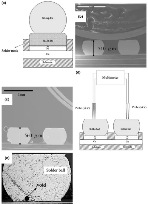
FIG. 1. Cross-sectional features of the samples: (a) the sketch of the Sn–Ag–Cu/Sn–Zn–Bi sample before reflow, (b) the Sn–Ag–Cu solder ball joint, (c) the Sn–Ag–Cu/Sn–Zn–Bi joint, (d) schematic illustration of sample resistance test, and (e) void formation in the Sn–Ag–Cu/Sn–Zn–Bi sample.
solder paste was composed of activated flux and Sn–Zn– Bi solder particles (20–25 m in diameter). The solder balls were 760 m in diameter. Prior to the soldering process, the solder paste with a thickness of 200m was stencil printed onto Cu/electrolytic Ni/Au metallized pad on the commercial BGA substrate, followed by solder ball attachment on the paste-covered pad, as shown in Fig. 1(a). The copper layer was 30m in thickness, and the thicknesses of the nickel and gold layers were 7 and 1m, respectively. In addition to the Sn–Ag–Cu/Sn–Zn– Bi joint, the Sn–Ag–Cu joint without paste was studied for comparison. Multiple reflow was conducted for 1, 5, and 10 cycles. Thermal treatment was performed at 150 °C for 100, 200, 500, and 1000 h The reflow experi-ment was performed in an infrared (IR) furnace under a protective atmosphere of 90%N2–10%H2. The reflow profile consisted of an activation stage at 170 °C with a peak temperature of 210 °C (for Sn–Ag–Cu/Sn–Zn–Bi samples) or 240 °C (for Sn–Ag–Cu samples) for 30 s and then a descent to room temperature over 3–4 min. Please note that Sn–Zn–Bi paste melts whereas Sn–Ag–Cu sol-der ball maintains solid at 210 °C peak temperature.
Electrical properties of the joints were evaluated by measuring the four-point contact resistance. The instru-ment used for electrical resistance measureinstru-ment was a HP3458A multimeter (Hewlett Packard) with a four-point-probe measurement function. Each resistance value showed on this study was the average of 30 testing data, 10 measurements taken for each specimen. For ease of measuring, the solder of the reflowed samples was ground with the No. 1200 sandpaper to a platform, as shown in Figs. 1(b) and 1(c). The probes, contacting with every two adjacent platforms of solder balls, were tested as closely to the center of the platform as possible. A schematic illustration of the sample resistance test is shown in Fig. 1(d). The heights of the reflowed samples after being grinded were roughly 510 m (Sn–Ag–Cu cases) and 560 m [Sn–Ag–Cu/Sn–Zn–Bi cases in which the void was clarified, as shown in Fig. 1(e)]. The resistance measurement was taken soon after grinding to avoid extensive oxidation.
The BGA specimens were also mounted, ground with diverse sandpapers, and polished with 0.3 m Al2O3 powder for cross-sectional investigation by scanning electron microscopy (SEM), energy dispersive x-ray analysis (EDX), and electron probe microanalysis (EPMA).
III. EXPERIMENTAL RESULTS
A. Microstructural evolution and electrical property of the reflowed joints
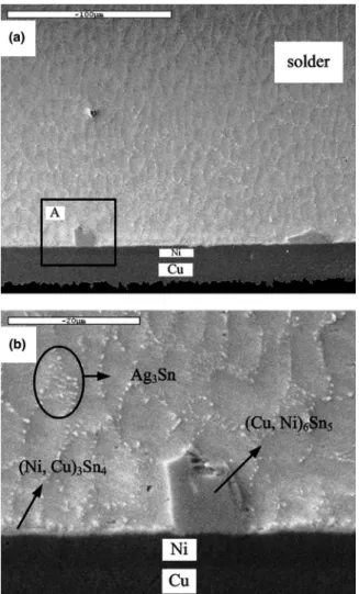
Figure 2(a) shows the SEM micrographs of both the solder bulk and the interface between Sn–Ag–Cu solder
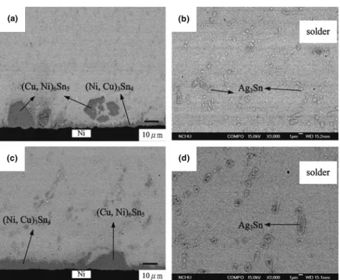
and Cu/Ni BGA substrate after single reflow cycle. Dur-ing reflow solderDur-ing, the topmost Au layer dissolves into the molten solder, leaving the Ni layer exposed to the molten solder. According to the EDS results, the inter-facial reaction between molten solder and the Ni layer results in the formation of pyramid-shaped (Cu, Ni)6Sn5 and layered (Ni, Cu)3Sn4, roughly 1.4 m thick, as shown in Fig. 2(b), a magnification of region A in Fig. 2(a). The microstructure of the bulk material, shown in Figs. 2(a) and 2(b), denotes the darker regions of Sn–rich areas, which are surrounded by brighter particle-sized Ag3Sn intermetallic compounds.
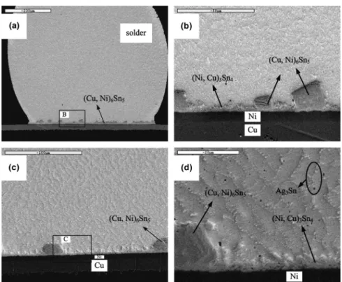
13,23–25 Figures 3(b) and 3(d), magnifications of region B and region C respectively shown in Figs. 3(a) and 3(c) indi-cate that as the increasing reflow goes from 5 [Fig. 3(a) and 3(b)] to 10 [Figs. 3(c) and 3(d)] cycles, the interfacial (Ni, Cu)3Sn4 grows further, toward 4.2 m thick, as shown in Fig. 3(d). Neither the pyramid-shaped (Cu, Ni)6Sn5nor the particle-sized Ag3Sn, in the bulk region, illustrated in Figs. 3(c) and 3(d), shows the significant
FIG. 2. Images of the Sn–Ag–Cu samples soldered at 240 °C: (a) the cross-section image after single reflow cycle and (b) the magnification of region A in (a).
grain growth, showing the similar microstructure to that in the single reflow sample, as shown in Figs. 2(a) and 2(b).
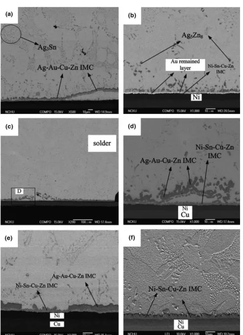
Figure 4(a) shows the SEM micrographs of both the solder bulk and the interface between Sn–Ag–Cu/Sn– Zn–Bi solder materials and the Cu/Ni/Au BGA substrate after single reflow cycle. The reflow results in counter interaction between the solid Sn–Ag–Cu solder ball and the liquid Sn–Zn–Bi solder paste. The two solders have mixed together and do not have a visible interfacial boundary. In the light of the previous study,26a relatively thick layer compound shown in Fig. 4(a), partly detached from the interface, is composed of Ag, Au, Cu, and Zn with varying elemental distribution forms near the inter-face. Furthermore, there exists the discontinuous IMC which consists of Ni, Sn, Cu, and Zn and forms at the interface between the Cu/Ni/Au metallization layers and solder, as shown in Fig. 4(b). Cu involves in N–Sn–Cu– Zn compounds locally.26
The remaining Au layer, ob-served at the interface, indicates that the interfacial reac-tion does not result in the exhausreac-tion of gold during the soldering process at 210 °C. As for the solder region, the needle-shaped Ag5Zn8 and Ag3Sn compounds are ob-served, as shown in Figs. 4(a) and 4(b). Bi is obviously observed in the lower part of the solder joints and distributes uniformly and does not precipitate or associ-ate with any compound after single reflow.26
Figures 4(c) and 4(d) and Figs. 4(e), and 4(f) show the SEM micrographs of both the solder bulk and the
inter-face between Sn–Ag–Cu/Sn–Zn–Bi solder materials and the Cu/Ni BGA substrate after 5 and 10 reflow cycles, respectively. Figure 4(d), a magnification of re-gion D in Fig. 4(c), shows that the Au layer is no longer observed at the interface, while the Ni–Sn–Cu–Zn com-pounds (mainly consist of Ni and Sn) grow significantly after 5 reflow cycles, toward 2–3 m. At 10 reflow cycles, the relatively thick Ag–Au–Cu–Zn layer shows an inclination to decrease, shown in Fig. 4(e), or even shrinks to disappear, shown in Fig. 4(f). The tendency of Ag–Au–Cu–Zn IMC shrinkage is not clarified here and the related studies are in progress. In addition, Bi accu-mulates after 10 cycles.26 The EDS mapping analysis [Figs. 5(a)–5(e)], shows that the coarsened elongated in-termetallic compounds located in the solder region are Ag3Sn. Besides, the contents of Cu and Zn are much less than those of Ag or Sn, nor are they embedded within Ag3Sn. Not only does Ag exist in Ag3Sn compounds (higher Ag concentration) but it is also observed in the solder region (lower Ag concentration).
The electrical resistance (Fig. 6) of Sn–Ag–Cu (la-beled SAC) and Sn–Ag–Cu/Sn–Zn–Bi (la(la-beled SAC + SZB) samples appears to show that the reflow tends to increase the electrical resistance. The average resis-tance values of Sn–Ag–Cu and Sn–Ag–Cu/Sn–Zn–Bi samples are respectively from 7.1 (single reflow) to 7.3 (10 cycles) m⍀ and from 7.2 (single reflow) to 7.6 (10 cycles) m⍀, indicating a 4–6% increase. It is also noticeable that the Sn–Ag–Cu/Sn–Zn–Bi samples
FIG. 3. Images of the Sn–Ag–Cu samples soldered at 240 °C: (a) the cross-section image after 5 reflow cycles, (b) the magnification of region B in (a), (c) the cross-section image after 10 reflow cycles, and (d) the magnification of region C in (c).
exhibit higher resistance than those of Sn–Ag–Cu samples. The explanation to this behavior will be dis-cussed later in Section IV.
B. Microstructural evolution and electrical property of the thermally aged joints
Figures 7(a) and 7(b) and Figs. 7(c) and 7(d), respec-tively, show the SEM micrographs of the solder bulk and the interface between Sn–Ag–Cu solder and Cu/Ni BGA substrate after heat treat of 100 and 1000 h. During the long term thermal aging toward 1000 h, the (Ni, Cu)3Sn4 compounds at the interface [Figs. 7(a) and 7(c)] and Ag3Sn in the solder region [Figs. 7(b) and 7(d)] show the
grain growth behavior, while the (Cu, Ni)6Sn5 com-pounds [shown in Figs. 7(a) and 7(c)] appear not to coarsen substantially.
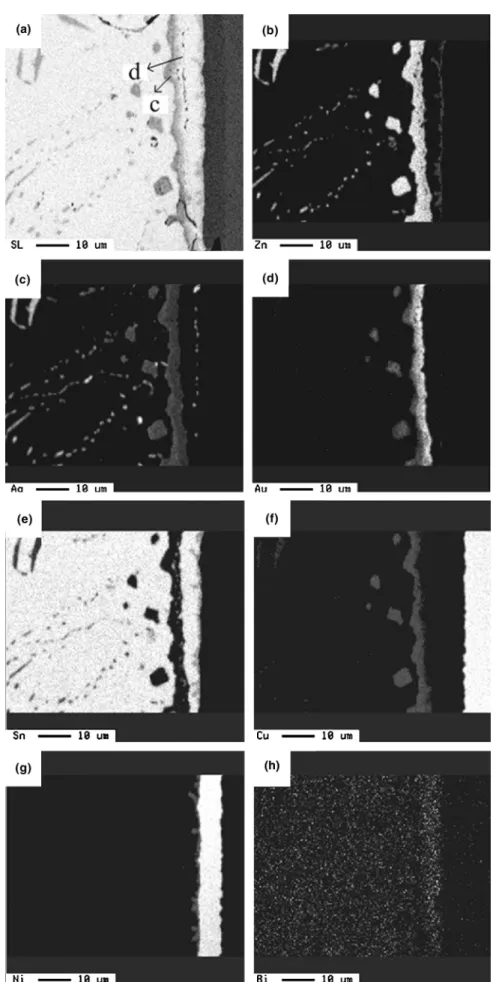
Figure 8(a) shows the SEM micrographs of both the solder bulk and the interface between Sn–Ag–Cu/Sn– Zn–Bi solder materials and Cu/Ni BGA substrate after heat treat of 100 h at 150 °C. Slightly different from the microstructure of the single reflow sample,26the elemen-tal mapping analysis [Figs. 8(b)–8(h)] reveals that at the interface exists continuous but zigzag IMC nodules, con-sisting of Ni, Sn, and Zn. Nevertheless, Cu, observed locally in Ni–Sn–Cu–Zn compounds after single reflow, is hardly identified in Ni–Sn–Zn zigzag compounds. The
FIG. 4. Images of the Sn–Ag–Cu/Sn–Zn–Bi samples soldered at 210 °C, (a, b) cross-section images after single reflow cycle, (c) the cross-section image after 5 reflow cycles, (d) the magnification of region D in (c), (e, f) cross-section images after 10 reflow cycles.
Au diffuses outward while the layered Ni–Sn–Zn com-pounds distributes, with varying distribution of Ag. Fur-thermore, the needle-shaped Ag–Zn–Sn and Ag5Zn8 compounds observed in the solder region of single reflow sample is also identified after 100 h aging test. A rela-tively thick layer compound composed of Ag, Au, Cu, and Zn with varying elemental distribution forms near the interface. It seems to show that Ag–Sn IMC particles are embedded within this compound layer. Bi distributes uniformly in the solder and does not associate with any compound. The region between the Ag–Au–Cu–Zn and the Ni–Sn–Zn compound layers consists of Sn and Bi only, indicating that Zn of the Sn–8Zn–3Bi solder paste migrates outward and inward completely to form the IMCs. The EDS results show that composition ratio of the Ag–Au–Cu–Zn compounds c (farther from the inter-face) and d (closer to the interinter-face) are, respectively, Ag:Au:Cu:Zn ⳱ 12:8:20:60 and 7:16:15:62 (at.%),
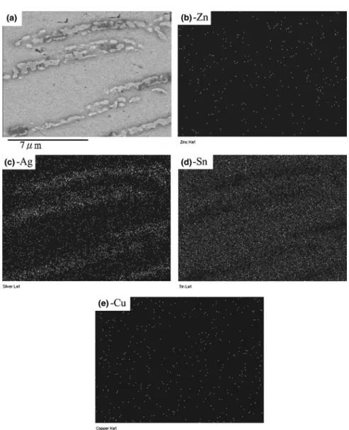
FIG. 5. Elemental analysis in the solder area of the sample soldered at 210 °C after 10 reflow cycles: (a) backscattered electron image, (b) Zn, (c) Ag, (d) Sn, and (e) Cu.
FIG. 6. Effect of reflow cycles on electrical resistance of solder joints
which correspond to the EPMA results for Ag, Au, and Cu elemental distributions of the layer IMCs in Figs. 8(c), 8(d), 8(f). The composition ratio of the Ni– Sn–Zn compound layers are not identified due to its thin crystal layer of less than 1m thick.
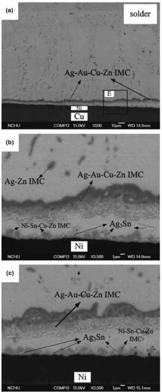
Figure 9(b), a magnification of region E in Fig. 9(a), and Fig. 9(c) shows the noticeable Ag3Sn grain growth near or at the interface after heat treatment of 200 and 500 h. Parts of the Ag3Sn are embedded in the Ni–Sn–Cu–Zn compound (roughly Ni:Sn:Cu:Zn ⳱ 28:45:9:18 at.%, mainly consisting of Ni and Sn), which does not show the significant zigzag nodule growth, and neither do the lay-ered Ag–Au–Cu–Zn compounds thicken, after heat treatment of 500 h. However, the appearance of the Ni–Sn–Cu–Zn compounds transforms from the separate zigzag nodules into the smoother uniform layer [shown in Fig. 10(a), marked with a black-dash line], indicating that the nodule Ni–Sn–Cu–Zn compounds tend to grow between the gaps as the aging time increases toward 1000hrs. Figures 10(a)–10(c) illustrate the micrographs of the Sn–Ag–Cu/Sn–Zn–Bi sample aged at 150 °C for 1000 h. The interfacial Ag3Sn, shown in Fig. 10(a), seems to coarsen to a size of around 2m. In the solder region, the elongated dispersed Ag3Sn (2–5 m) and Ag5Zn8(4–6m), respectively shown in Figs. 10(b) and Fig. 10(c), are observed. The Ag3Sn compounds grow with the aging time. Moreover, Bi is not contained within the compounds or precipitates in the solder region after 1000 h long term aging.
The electrical resistances of Sn–Ag–Cu (labeled SAC) and Sn–Ag–Cu/Sn–Zn–Bi (labeled SAC + SZB) samples as a function of the aging time are shown in Fig. 11. For both solder joints, the electrical resistance increases with aging time. The average resistance values of Sn–Ag–Cu and Sn–Ag–Cu/Sn–Zn–Bi samples are re-spectively from 7.1 (aging 0 h) to 7.8 (aging 1000 h) m⍀ and from 7.2 (aging 0 h) to 7.9 (aging 1000 h) m⍀, show-ing an increase of 9–9.8%. Like the results in multiple reflowed samples, the average resistance values of Sn–Ag–Cu/Sn–Zn–Bi samples are higher than those of Sn–Ag–Cu samples.
IV. DISCUSSION
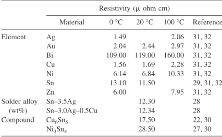
The electrical properties of a solder joint in such elec-tronic packages as ball-grid array, flip-chip, or surface-mount joints, are influenced by several factors, such as interfacial reactions, solder composition, surface finish (or under-bump metallization), solder volume, reflow conditions, and some others.27 In this study, the major goal concentrates on the microstructural evolution of the solder joint on electrical resistance of the Sn–Ag–Cu and Sn–Ag–Cu/Sn–Zn–Bi joints under various testing condi-tions. Table I22,27–32lists the electrical resistivities of the solder alloys, elements and related intermetallic com-pounds. The formation of the Ni–Sn (Ni3Sn4) or Cu–Sn (Cu6Sn5) compound leads to a higher resistivity value
FIG. 7. Cross-section images of the Sn–Ag–Cu samples aged at different time: (a) 100 h (at the interface), (b) 100 h (in the solder area), (c) 1000 h (at the interface), and (d) 1000 h (in the solder area).
FIG. 8. Elemental analysis at the interfacial area of the specimen soldered at 210 °C after 100 h aging at 150 °C: (a) backscattered electron image (c farther from the interface and d closer to the interface), (b) Zn, (c) Ag, (d) Au, (e) Sn, (f ) Cu, (g) Ni, and (h) Bi.
than that of Ni, Sn, or Cu itself. The resistances of in-termetallic compounds are usually higher than those of high Sn-containing solder alloys.27,28,33,34 Under both multiple cycles and heat-treatment testing conditions, the electrical resistances of Sn–Ag–Cu/Sn–Zn–Bi and Sn– Ag–Cu samples show an increasing trend, as shown in
Figs. 6 and 11. The microstructure of the Sn–Ag–Cu samples, under various multiple cycles, shown in Figs. 2(a) and 2(b) and Figs. 3(a)–3(d), indicates that the interfacial (Ni, Cu)3Sn4 compounds, which are the Ni3Sn4 with Cu dissolution, coarsen with the reflow cycles, while the (Cu, Ni)6Sn5compounds do not grow significantly. On the other hand, the Ag3Sn in the solder
FIG. 9. Cross-section images of the Sn–Ag–Cu/Sn–Zn–Bi samples aged at different time: (a) 200 h (at the interface), (b) the magnification of region E in (a), and (c) 500 h (at the interface).
FIG. 10. Cross-section images of the Sn–Ag–Cu/Sn–Zn–Bi samples aged at 1000 h (a) at the interface and (b, c) in the solder areas.
region appears not to grow substantially. Consequently, coarsened (Ni, Cu)3Sn4 may play a crucial role in the gradually increasing resistance. The Sn–Ag–Cu solder ball used in this study and the Ni metallization are of constant volume. In other words, the contents of Sn, Ag, Cu, Ni, and Au are fixed and limited in the batch-type solder system. The gradually grown (Ni, Cu)3Sn4 com-pounds of higher resistivity are attributed to the con-sumption of the low resistivity Ni, Cu, and Sn. As the reflow or heat treatment proceeds, the amount of (Ni, Cu)3Sn4compound in the solder joint increases while the element contents of Cu, Ni, and Sn do the reverse since they form in compounds. As a result, based on the results of Table I, the increasing amount of Ni–Sn compound of higher resistivity possibly indicates the slightly rising resistance values of the joints.
The electrical resistances of Sn–Zn–Bi/Sn–Ag–Cu samples under various reflow cycles, similar to the ten-dency of the Sn–Ag–Cu samples, show several different behaviors in addition to the grain growth of Ni– Sn contained compounds at the interface. As the reflow cycles increase, the Au layer, shown in Fig. 4(b),
diffuses outward from the interface and involves in the formation of Ag–Au–Cu–Zn compounds.26 The ex-hausted Au layer leads to the exposure of the Ni metallization, then resulting in the Ni–Sn–Cu–Zn forma-tion, as shown in Figs. 4(d)–4(f). According to the results shown in Table I, the resistivity of Au is much lower than Sn or high Sn-containing solder materials, and the ex-haustion of Au, together with the grown Ni–Sn–Cu–Zn compounds, are possibly responsible for the increasing resistance value of the samples. However, microstructure of the 10 reflow cycle samples changes significantly. The Ag–Au–Cu–Zn compounds seem to decompose near the interface, while the Ni–Sn–Cu–Zn compounds keep coarsening at the interface, as shown in Figs. 4(e) and 4(f). The decomposition of Ag–Au–Cu–Zn and the growth of Ni–Sn–Cu–Zn may counteract the fluctuation of resistances of Sn–Zn–Bi/Sn–Ag–Cu samples. The rea-son for the decomposition of the Ag–Au–Cu–Zn com-pounds is not clear now and needs further investigation. The Ag and Sn surrounded the Ag3Sn in the 10 reflow cycle solder ball shown in Figs. 5(a)–5(e) might serve as a source for the growth of Ag3Sn compounds. The growth of Ag3Sn at the expense of Ag and Sn contributes to the increasing resistance values of Sn–Zn–Bi/Sn–Ag– Cu samples after 10 reflow cycles.
Generally, long term solid–solid interaction may result in the compound growth. The increase of electrical re-sistances of the Sn–Ag–Cu samples with heat-treatment might be ascribed to the grain growth of the (Ni, Cu)3Sn4 compounds at the interface and Ag3Sn in the solder re-gion, while the (Cu, Ni)6Sn5 compounds appear not to coarsen substantially, as shown in Figs. 2(a)–2(b) and Figs. 7(a)–7(d). It happens that similar behavior occurs for Sn–Zn–Bi/Sn–Ag–Cu samples under heat treatment, as shown in Figs. 4(a), 9(a)–9(c), 10(a)–10(c).
Several factors might affect the electrical resistances of the samples. First of all, the outward diffusion of the Au layer, shown in Fig. 4(b) (after single reflow, or 0 h heat treatment) during long term thermal aging, leads to the exposure of the Ni metallization and the formation of Ni–Sn–Cu–Zn, as shown in Figs. 8(a), 9(b), 9(c), and 10(a). Secondly, the formation of a uniform Ni–Sn–Cu– Zn compound layer may raise the electrical resistance values after 1000 h thermal aging, as shown in Figs. 8(a) and 10(a). Finally, the distribution and coarsening of Ag3Sn [Figs. 10(b) and 10(c)], during the solid-solid in-teraction at 150 °C in the upper part of the solder may also increase the electrical resistance.
It is noticed that the electrical resistance value of Sn–Zn–Bi/Sn–Ag–Cu samples is higher than that of Sn–Ag–Cu samples in all cases. This observation may be ascribed to several reasons. The volume of solder applied for Sn–Ag–Cu is less than that of Sn–Zn–Bi/Sn–Ag–Cu. Figures 1(b) and 1(c) clearly indicate that the height of the Sn–Zn–Bi/Sn–Ag–Cu solder joint is roughly 50 m
TABLE I. Resistivity of specified elements, alloys, and compounds at various temperatures. Resistivity ( ohm cm) Material 0 °C 20 °C 100 °C Reference Element Ag 1.49 2.06 31, 32 Au 2.04 2.44 2.97 31, 32 Bi 109.00 119.00 160.00 31, 32 Cu 1.56 1.69 2.28 31, 32 Ni 6.14 6.84 10.33 31, 32 Sn 13.10 11.50 29, 31, 32 Zn 6.00 7.95 31, 32 Solder alloy Sn–3.5Ag 12.30 28
(wt%) Sn–3.0Ag–0.5Cu 12.34 28 Compound Cu6Sn5 17.50 22, 30
Ni3Sn4 28.50 27, 30
FIG. 11. Effect of aging time on electrical resistance of solder joints.
higher than that of the Sn–Ag–Cu solder joint. The greater solder volume possibly gives rise to the higher electrical resistance. Besides, it is well known that the voids are usually identified during the soldering process as the solder paste is used as the joint materials. Hence, the voids appearing in the Sn–Zn–Bi/Sn–Ag–Cu solder joint might contribute to the increasing electrical resis-tance, as shown in Fig. 1(e). Furthermore, the electrical resistivity (Table I) of Bi (110 ⍀ cm) is significantly higher than that of any listed metal, alloy or compound. The addition of Bi dispersed in the solder will certainly raise the electrical resistance of the Sn–Zn–Bi/Sn–Ag– Cu solder joint compared with Sn–Ag–Cu joints (without Bi addition). Yet we have insignificant information about the effect of Bi accumulation on electrical resistance of Sn–Ag–Cu/Sn–Zn–Bi samples after 10 cycles.
V. CONCLUSION
The microstructural evolution along with the electrical resistance variation of the Sn–Ag–Cu or Sn–Ag–Cu/Sn– Zn–Bi joints was examined under various reflow and heat-treatment conditions. For both types of solder joint, the electrical resistance generally increases with reflow cycles and aging time. The average resistance values of Sn–Ag–Cu and Sn–Ag–Cu/Sn–Zn–Bi samples respec-tively increase from 7.1 to 7.3 m⍀ and 7.2 to 7.6 m⍀ as the reflow cycle increases up to 10. Heat treatment up to 1000 h also increases the electrical resistance of Sn–Ag– Cu and Sn–Ag–Cu/Sn–Zn–Bi samples, respectively, from 7.1 to 7.8 m⍀ and 7.2 to 7.9 m⍀. The incorporation of Sn–Zn–Bi raises the electrical resistance of the joint, although it allows the joining of Sn–Ag–Cu at a rela-tively low temperature of 210 °C. The reason for the electrical resistance variation is ascribed to the micro-structural variation and to the Bi inclusion.
ACKNOWLEDGMENT
The financial support for this work, provided by the National Science Council of the Republic of China (Tai-wan) under Grant No. NSC91-2216-E-006-035, is grate-fully acknowledged. The authors also thank Accurus Sci-entific Co., LTD, Taiwan, for supplying the solder balls.
REFERENCES
1. X. Huang, S-W.R. Lee, C.C. Yan, and S. Hui: Characterization and analysis on the solder ball shear testing conditions, electronic components and technology conference, in 2001 Proceedings, 51st, 29th May–1st June 2001, Orlando, FL, pp. 1065–1071. 2. Y.C. Chan, P.L. Tu, C.W. Tang, K.C. Hung, and J.K. Lai:
Reli-ability studies ofBGA solder joints—Effect of Ni–Sn interme-tallic compound. IEEE Trans. Adv. Pkg. 24, 25 (2001). 3. T. Sugizaki, H. Nakao, T. Kimura, and T. Watanabe: BGA
joint-ing property of Sn–8.8 mass% Zn and Sn–8.0 mass% Zn–3.0
mass% Bi Solder on electroless nickel-phosphorus/immersion gold plated substrates. Mater. Trans. 44, 1790 (2003).
4. C.B. Lee, S.B. Jung, Y.E. Shin, and C.C. Shur: Effect of iso-thermal aging on ball shear strength in BGA joints with Sn–3.5Ag–0.75Cu solder. Mater. Trans. 43, 1858 (2002). 5. C.B. Lee, I.Y. Lee, S.B. Jung, and C.C. Shur: Effect of surface
finishes on ball shear strength in BGA joints with Sn–3.5 mass% Ag solder. Mater. Trans. 43, 751 (2002).
6. K. Uenishi, Y. Kohara, S. Sakatani, T. Saeki, K.F. Kobayashi, and M. Yamamoto: Melting and joining behavior of Sn/Ag and Sn–Ag/Sn–Bi plating on Cu core ball. Mater. Trans. 43, 1833 (2002).
7. M. Nishiura, A. Nakayama, S. Sakatani, Y. Kohara, K. Uenishi, and K.F. Kobayashi: Mechanical strength and microstructure of BGA joints using lead-free solders, Mater. Trans. 43, 1802 (2002).
8. M. Amagai, M. Watanabe, M. Omiya, K. Kishimoto, and T. Shibuya: Mechanical characterization of Sn–Ag-based lead-free solders. Microelectron. Reliab. 42, 951 (2002).
9. A. Hirose, T. Fujii, T. Imamura, and K.F. Kobayashi: Influence of interfacial reaction on reliability of QFP joints with Sn–Ag based Pb free solders. Mater. Trans. 42, 794 (2001).
10. Y. Miyazawa and T. Ariga: Influences of aging treatment on mi-crostructure and hardness of Sn–(Ag, Bi, Zn) eutectic solder al-loys. Mater. Trans. 42, 776 (2001).
11. J. Wu and M.G. Pecht: Contact resistance and fretting corrosion of lead-free alloy coated electrical contacts, in International IEEE Conference on Asian Green Electronics (AGEC) (2004), pp. 127–135.
12. Y. Chonan, T. Komiyama, J. Onuki, R. Urao, T. Kimura, and T. Nagano: Influence of P content in electroless plated Ni–P alloy film on interfacial structures and strength between Sn–Zn solder and plated Au/Ni–P alloy film. Mater. Trans. 43, 1887 (2002). 13. C.M. Chuang, P.C. Shih, and K.L. Lin: Mechanical strength of
Sn–3.5Ag-based solders and related bondings. J. Electron. Mater.
33,1 (2004).
14. J.W. Choi, H.S. Cha, and T.S. Oh: Mechanical properties and shear strength of Sn–3.5Ag–Bi solder alloys. Mater. Trans. 43, 1864 (2002).
15. J.W. Jang, D.R. Frear, T.Y. Lee, and K.N. Tu: Morphology of interfacial reaction between lead-free solders and electroless Ni–P under bump metallization. J. Appl, Phys. 88, 6359 (2000). 16. E. Bradley III and J. Hranisavljevic: Characterization of the
melt-ing and wettmelt-ing of Sn–Ag–X solders, in Proceedmelt-ings of the 50th Electronic Components and Technology Conference, Las Vegas, NV (2000), pp. 1443–1448.
17. P.T. Vianco and J.A. Rejent: Properties of ternary Sn–Ag–Bi sol-der alloys: Part I. Thermal properties and microstructural anaylsis. J. Electron. Mater. 28, 1127 (1999).
18. P.T. Vianco and J.A. Rejent: Properties of ternary Sn–Ag–Bi sol-der alloys: Part II. Wettability and mechanical properties anaylsis. J. Electron. Mater. 28, 1138 (1999).
19. Y. Kariya and M. Otsuka: Effect of bismuth on the isothermal fatigue properties of Sn–3.5mass% Ag solder alloy. J. Electron. Mater. 27, 866 (1998).
20. M. Abtew and G. Selvaduray: Lead-free solders in microelectron-ics. Mater. Sci. Eng. R 27, 95 (2000).
21. S.K. Kang, W.K. Choi, D.Y. Shih, P. Lauro, D.W. Henderson, T. Gosselin, and D.N. Leonard: Interfacial reactions, microstruc-ture and mechanical properties of Pb-free solder joints in PBGA laminates, in Proceedings of the 52nd Electronic Components and Technology Conference, San Diego, CA, pp. 146–153.
22. C.N. Liao and C.T. Wei: Effect of intermetallic compound for-mation on electrical properties of Cu/Sn interface during thermal treatment. J. Electron. Mater. 33, 1137 (2004).
23. S. Ahat, M. Sheng, and L. Luo: Microstructure and shear strength evolution of SnAg/Cu surface mount solder joint during aging. J. Electron. Mater. 30, 1317 (2001).
24. M. He, Z. Chen, and G. Qi: Solid state interfacial reaction of Sn–37Pb and Sn–3.5Ag solders with Ni–P under bump metalli-zation. Acta Mater. 52, 2047 (2004).
25. J.H.L. Pang, B.S. Xiong, C.C. Neo, X.R. Zhang, and T.H. Low: Bulk solder and solder joint properties for lead free 95.5Sn–3.8Ag–0.7Cu solder alloy, in Proceedings of the 53rd Electronic Components and Technology Conference, New Or-leans, LA (2003), pp. 673–679.
26. P.C. Shih and K.L. Lin: Interfacial bonding behavior with intro-duction of Sn–Zn–Bi paste to Sn–Ag–Cu ball grid array package during multiple reflows. J. Mater. Res. 20, 219 (2005). 27. S.K. Kang, W.K. Choi, M.J. Yim, and D.Y. Shih: Studies of the
mechanical and electrical properties of lead-free solder joints. J. Electron. Mater. 31, 1292 (2002).
28. B.A. Cook, I.E. Anderson, J.L. Harringa, and R.L. Terpstra: Effect of heat treatment on the electrical resistivity of near-eutectic Sn–Ag–Cu Pb-free solder alloys. J. Electron. Mater. 31, 1190 (2002).
29. S.K. Kang, J. Horkans, P.C. Andricacos, R.A. Carruthers, J. Cotte, M. Datta, P. Gruber, J.M.E. Harper, K. Kwietniak, C. Sambucetti, L. Shi, G. Brouillette, and D. Danovitch: Pb-free solder alloys for flip chip applications, in Proceedings of the 49th Electronic Com-ponents and Technology Conference San Diego, CA (1999), pp. 283–288.
30. H.P.R. Frederikse, R.J. Fields, and A. Feldman: Thermal and elec-trical properties of copper-tin and nickel-tin intermetallics. J. Appl. Phys. 72, 2879 (1992).
31. F. Seitz: The Modern Theory of Solids (McGraw-Hill, New York, 1940), pp. 10–12.
32. Handbook of Chemistry and Physics, 43rd ed. (Chemical Rubber Publishing, 1961), pp. 2626–2633.
33. B.S. Chiou, K.C. Liu, J.G. Duh, and P.S. Palanisamy: Intermetal-lic formation on the fracture of Sn/Pb solder and Pd/Ag conductor interfaces. IEEE Trans. Comp., Hybrids Mfg. Technol. 13, 267 (1990).
34. J.W. Yoon, S.W. Kim, J.M. Koo, D.G. Kim, and S.B. Jung: Re-liability investigation and interfacial reaction of ball-grid-array packages using the lead-free Sn–Cu solder. J. Electron. Mater. 33, 1190 (2004).