Effects of Mg incorporation on the optical properties of ZnO prepared by the sol-gel method
Yow-Jon Lin,1,a兲Ping-Hsun Wu,1Chia-Lung Tsai,2Chia-Jyi Liu,2Zhi-Ru Lin,2 Hsing-Cheng Chang,3and Ching-Ting Lee4
1Institute of Photonics, National Changhua University of Education, Changhua 500, Taiwan
2Department of Physics, National Changhua University of Education, Changhua 500, Taiwan
3Department of Automatic Control Engineering, Feng Chia University, Taichung 407, Taiwan
4Institute of Microelectronics, Department of Electrical Engineering, National Cheng-Kung University, Tainan 701, Taiwan
共Received 14 January 2008; accepted 8 April 2008; published online 10 June 2008兲
ZnO films with and without Mg doping 共Zn1−xMgxO兲 were deposited on substrates by the sol-gel technique. X-ray photoelectron spectroscopy, x-ray diffraction, photoluminescence, and conductivity measurements were used to characterize the Zn1−xMgxO semiconductors. It is worth noting that the intensity of the band-edge luminescence共BEL兲 of the Zn0.973Mg0.027O film at room temperature was nearly six times the ZnO film. The enhanced BEL intensity has been attributed to the suppression of capacitance variation related to trapping/detrapping of charges, a decrease in the number of nonradiative recombination defects, and an increase in the nonradiative recombination lifetime. © 2008 American Institute of Physics.关DOI:10.1063/1.2939255兴
I. INTRODUCTION
ZnO represents an alternate candidate for use in opto- electronic application in the short wavelength range共green, blue, and ultraviolet兲 because ZnO displays a wide band gap 共⬃3.3 eV兲 comparable to other wide gap semiconductors, such as GaN and SiC.1–4ZnO is another candidate for high transparent contact material. Nakahara et al.5 reported that Ga-doped ZnO was fabricated to serve as p-contacts of InGaN-based light-emitting diodes共LEDs兲. Park et al.6pre- sented the application of ZnO for the anode film of organic LEDs. Several recent papers have reported ZnO-based LEDs.7–11 Yuen et al.7 suggested that the ultraviolet elec- troluminescence 共EL兲 from the n-type ZnO:Al/p-type SiC heterojunction originated from the exciton-exciton scattering inside the n-type ZnO:Al film. Alivov et al.8 suggested that the observed EL from n-type GaN/n-type ZnO/p-type GaN LEDs is most probably a superposition of emission originat- ing from n-type ZnO, n-type GaN, and p-type GaN layers.
Alivov et al.9reported that the 389 nm emission for n-type ZnO/p-type AlGaN heterojunction LEDs is shown to origi- nate from recombination within the ZnO. Jang et al.10 pointed out that the emission for n-type ZnO/p-type ZnO LEDs is mainly from the region close to the p layer. Accord- ing to the reported results,7–10 we find that the brightness of ZnO-based LEDs is deeply related to the optical property of ZnO. In this paper, we report the preparation of ZnO films doped with and without Mg on glass共or Si兲 substrates using a sol-gel spin-coating technique. We find that using Mg dop- ing improves the band-edge luminescence共BEL兲 of ZnO be- cause of the suppression of capacitance variation共related to trapping/detrapping of charges兲 determined in hysteresis-
-type current-voltage 共I-V兲 characteristics. The sol-gel chemical deposition technique is very attractive as it can be easily implemented in a laboratory for the deposition of semiconducting thin films.12,13 This sol-gel technique offers the possibility of preparing a small—as well as large—area coating of ZnO thin films at low cost for technological applications.12
II. EXPERIMENT PROCEDURE
ZnO films with and without Mg doping 共Zn1−xMgxO兲 were prepared by the sol-gel method. For ZnO films, Zn共CH3COO兲2· H2O was added to 20 ml methanol, KOH was added to 20 ml methanol to create the alkaline environ- ment 共pH ⬃9兲, and the resulting mixture was stirred at 50 ° C to yield a clear and homogeneous solution, which served as the coating solution after cooling to room temperature. For ZnO films with light Mg doping, Zn共CH3COO兲2· H2O and Mg共CH3COO兲2· H2O were added to 20 ml methanol, KOH was added to 20 ml methanol to create the alkaline environment 共pH ⬃9兲, and the resulting mixture was stirred at 50 ° C to yield a clear and homoge- neous solution, which served as the coating solution after cooling to room temperature. The solution was dropped onto Si or glass substrates, which were rotated at 3000 rpm for 20 s and rotated again at 5000 rpm for another 10 s. Si and glass substrates were ultrasonically cleaned for 10 min etch in acetone, then in methanol, followed by de-ionized water and dried in nitrogen before spin coating. After depositing by spin coating, the films were dried at 300 ° C for 10 min on a hotplate to evaporate the solvent and remove organic residu- als. The procedures from coating to drying were repeated many times. The films were then inserted into a furnace and annealed in air at 500 ° C for 4 h.. The film thickness was estimated from atomic force microscopy. X-ray diffraction 共XRD兲 and x-ray photoelectron spectroscopy 共XPS兲 were
a兲Electronic mail: [email protected].
JOURNAL OF APPLIED PHYSICS 103, 113709共2008兲
0021-8979/2008/103共11兲/113709/4/$23.00 103, 113709-1 © 2008 American Institute of Physics
Downloaded 07 Oct 2009 to 140.116.208.56. Redistribution subject to AIP license or copyright; see http://jap.aip.org/jap/copyright.jsp
employed to identify crystalline phases, surface morphology, x, and chemical bonding states in Zn1−xMgxO films. To de- termine the change in the atomic concentrations of the ele- ments 共i.e., Zn, O, and Mg兲 in the Zn1−xMgxO films, we obtained the peak area in the XPS spectra of Mg 1s, Zn 2p, and O 1s. The atomic concentrations of the elements were determined using the peak area and the atomic sensitivity factors of the elements. The concentration of Mg2+ was ad- justed to form Zn1−xMgxO thin films with x = 0 and x
= 0.027. In addition, using a Ne-Cu laser共the 248 nm line兲 as an excitation source, the photoluminescence共PL兲 band was observed for Zn1−xMgxO films at room temperature. From these results, the effect of Mg doping on the optical property of Zn1−xMgxO is discussed.
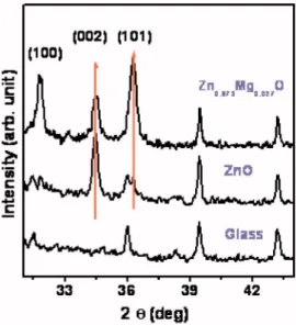
III. EXPERIMENTAL RESULTS AND DISCUSSION Figure 1 shows the XRD patterns of Zn0.973Mg0.027O films and ZnO films, respectively. An XRD pattern of glass is shown in Fig.1, owing to the deposition of Zn0.973Mg0.027O 共or ZnO兲 on glass substrates. It suggests a single phase for- mation having a hexagonal wurtzite structure with a pre- ferred c-axis orientation.13 No evidence of MgO phase was seen, confirming the monophasic nature of these composi- tions共Ghosh and Basak13 suggested that the solubility limit of MgO in Zn1−xMgxO in sol-gel deposited films lies in the composition range of 0.05⬍x⬍0.08.兲. Jung et al.14and Mat- sumura et al.15 reported that the 共200兲 peak due to a MgO bulk crystal with a rocksalt structure is located at 42.7°. Fig- ure 1 also shows a comparison of the XRD patterns from pure ZnO and from Zn0.973Mg0.027O films. By comparing the ZnO film, we can see that the 共002兲 peak slightly shifted toward the high angle for Zn0.973Mg0.027O films. Matsumura et al.15and Ohtomo et al.16 pointed out that the共002兲 peak shifts continuously to the higher angle side when x of Zn1−xMgxO increases, meaning that the lattice constant de- creases with an increase in x. Qiu et al.17 suggested that the
increase in 2 of共002兲 peak with an increase in Mg content indicates that the ionic radius of Mg2+is smaller than Zn2+. Thus, we deduce that a slight shift in the peak position of the 共002兲 peak may result from Mg doping.
Figure 2 shows the PL spectra of ZnO films and Zn0.973Mg0.027O films deposited on Si substrates, respec- tively. Two emission peaks at room temperature were noted.
The peak at ⬃3.4 eV is BEL.18 The green luminescence 共GL兲 关peak position at ⬃2.5 eV 共Refs. 18–20兲兴 is oxygen- vacancy-related emission.18,21 Based on the XPS result, we find that the O/共Zn+Mg兲 atomic concentration ratio in- creases from 0.92 to 1.04 for x of Zn1−xMgxO increasing from 0 to 0.027. Therefore, the enhanced GL intensity is not attributed to an increase in the number of oxygen-vacancy- related defects. In addition, the yield in the BEL intensity is seen to increase up to six fold for Zn0.973Mg0.027O. There- fore, we deduce that the enhanced PL intensity is attributed to a decrease in the number of nonradiative recombination defects and an increase in the nonradiative recombination lifetime 共nr兲. The radiative efficiency 共兲 is defined as
=关1+共r/nr兲兴−1.r is the radiative recombination lifetime.
Asnrincreases,increases. On the other hand, by compar- ing the ZnO film, we can see that BEL shifted toward the high photon energy by 0.07 eV for Zn0.973Mg0.027O films.
From recent optical studies of Zn1−xMgxO, the energy of the fundamental band-to-band transition was found to be strongly blueshifted with increasing Mg content.13,16,22
To demonstrate the effect of changes in the number of nonradiative recombination defects and nr on the optical property of ZnO films with and without Mg doping, we used a simple technique to measure changes in hysteresis-type I-V curves and the displacement current共Id兲. Ti/Au was used as the electrode, which was deposited on top of the ZnO films.
Ti/Au contacts were formed by an SC5750 sputter coater.
With Ir共Iras resistive part of the current兲, the total current is given by I = Ir+ Id. To note the change in Id, the ZnO film thickness was designed to be ⬃15 nm and the gap spacing 共d兲 between the Ti/Au contact pads was designed to be 3 cm. The thin ZnO film and the large d between the Ti/Au contact pads could lead to an increase in the total resistance and a reduction in Ir. Thus, the change in Id can be clearly observed. Smith and Forrest23stated that Idwas found in the
FIG. 1. 共Color online兲 XRD patterns of ZnO films, Zn0.973Mg0.027O films, and glass substrates.
FIG. 2.共Color online兲 PL spectra of ZnO films and Zn0.973Mg0.027O films.
113709-2 Lin et al. J. Appl. Phys. 103, 113709共2008兲
Downloaded 07 Oct 2009 to 140.116.208.56. Redistribution subject to AIP license or copyright; see http://jap.aip.org/jap/copyright.jsp
high-resistivity polymer film, meaning that Id is extremely low. Figure 3 shows hysteresis-type I-V curves for Au/Ti/ZnO/Ti/Au devices for 10 and 5 V loops. The I-V characteristics of the devices were measured with a Keithley model-4200 semiconductor characterization system. The sweep rate was 3.24 V/s. The voltage was incremented in steps of 0.2 V from −10 V共−5 V兲 to 10 V 共5 V兲 and in the reverse direction. In Fig.3, we find that I does not vanish at zero bias 共a positive current at zero bias for a sweep from negative to positive bias and a negative current at zero bias for the reverse sweep direction兲, owing to the presence of Id. Figure3 shows, with a sweep voltage of 10 V, that the cur- rent amplitude at V = 0 共during the sweep from 10 to
− 10 V or the sweep from −10 to 10 V兲 was higher than with a sweep voltage of 5 V and that the voltage amplitude at I
= 0共during the sweep from 10 to −10 V or the sweep from
−10 to 10 V兲 was higher than with a sweep voltage of 5 V, meaning that the contribution of capacitance variation 关V共dC/dt兲兴 on Id is therefore much stronger than that from voltage variation 关C共dV/dt兲兴.24 Id is represented by Id
=共d/dt兲共CV兲=V共dC/dt兲+C共dV/dt兲⬇V共dC/dt兲.25,26 Thus, the total current is given by I = Ir+ Id⬇Ir+ V共dC/dt兲. Based on this result, we deduce that capacitance variation is related to trapping/detrapping of charges within the ZnO film.
Similarly, Ti/Au was used as the electrode, which was deposited on top of the Zn0.973Mg0.027O films. To note the change in Id, the Zn0.973Mg0.027O film thickness was designed to be ⬃20 nm and the gap spacing between the Ti/Au contact pads was designed to be 2.5 cm. The inset of Fig. 3 shows hysteresis-type I-V curves for Au/Ti/Zn0.973Mg0.027O/Ti/Au devices for 10 and 5 V loops. Similarly, the sweep rate was 3.24 V/s. The inset of Fig.3 shows, with a sweep voltage of 10 V, that the current amplitude at V = 0 共during the sweep from 10 to −10 V or the sweep from −10 to 10 V兲 is close to that with a sweep voltage of 5 V and that the voltage amplitude at I = 0共during the sweep from 10 to − 10 V or the sweep from
−10 to 10 V兲 is close to that with a sweep voltage of 5 V, meaning that the contribution of voltage variation 关C共dV/dt兲兴 on Idis therefore much stronger than that due to
capacitance variation 关V共dC/dt兲兴.24 Id is represented by Id
=共d/dt兲共CV兲=V共dC/dt兲+C共dV/dt兲⬇C共dV/dt兲.25,26 Thus, the total current is given by I = Ir+ Id⬇Ir+ C共dV/dt兲. Based on this result, we suggested that trapping/detrapping of charges within the Zn0.973Mg0.027O film could be neglected.
This trend is attributed to light Mg doping possibly leading to the suppression of capacitance variation, a decrease in the number of nonradiative recombination defects, and an in- crease innr, resulting in an increase in the BEL intensity.
IV. CONCLUSIONS
In summary, the effect of Mg incorporation on the opti- cal properties of ZnO prepared by the sol-gel method has been demonstrated in the study. It is worth noting that the BEL intensity of the Zn0.973Mg0.027O film at room tempera- ture was nearly six times the ZnO film. The experimental results show that the enhanced BEL intensity is deeply re- lated to an increase innr, a decrease in the number of non- radiative recombination defects, and the suppression of ca- pacitance variation 共related to trapping/detrapping of charges兲 determined in hysteresis-type I-V characteristics.
ACKNOWLEDGMENTS
The authors acknowledge support in the form of grants from the National Science Council of Taiwan 共Contract No.
96-2112-M-018-001兲.
1S. J. Pearton, D. P. Norton, K. Ip, Y. W. Heo, and T. Steiner,Prog. Mater.
Sci.50, 293共2005兲.
2D. C. Look,Mater. Sci. Eng., B80, 383共2001兲.
3Y. J. Lin and C. L. Tsai,J. Appl. Phys.100, 113721共2006兲.
4Y. J. Lin, C. L. Tsai, Y. M. Lu, and C. J. Liu,J. Appl. Phys.99, 093501 共2006兲.
5K. Nakahara, K. Tamura, M. Sakai, D. Nakagawa, N. Ito, M. Sonobe, H.
Takasu, H. Tampo, P. Fons, K. Matsubara, K. Iwata, A. Yamada, and S.
Niki,Jpn. J. Appl. Phys., Part 243, L180共2005兲.
6S. H. K. Park, J. I. Lee, C. S. Hwang, and H. Y. Chu,Jpn. J. Appl. Phys., Part 244, L242共2005兲.
7C. Yuen, S. F. Yu, S. P. Lau, Rusli, and T. P. Chen,Appl. Phys. Lett.86, 241111共2005兲.
8Y. I. Alivov, Ü. Özgür, S. Doğan, C. Liu, Y. Moon, X. Gu, V. Avrutin, Y.
Fu, and H. Morkoç,Solid-State Electron.49, 1693共2005兲.
9Y. I. Alivov, E. V. Kalinina, A. E. Cherenkov, D. C. Look, B. M. Ataev, A.
K. Omaev, M. V. Chukichev, and D. M. Bagnall,Appl. Phys. Lett.83, 4719共2003兲.
10S. Jang, J. J. Chen, F. Ren, H. S. Yang, S. Y. Han, D. P. Norton, and S. J.
Pearton,J. Vac. Sci. Technol. B24, 690共2006兲.
11H. S. Yang, S. Y. Han, Y. W. Heo, K. H. Baik, D. P. Norton, S. J. Pearton, F. Ren, A. Osinsky, J. W. Dong, B. Hertog, A. M. Dabiran, P. P. Chow, L.
Chernyak, T. Steiner, C. J. Kao, and G. C. Chi,Jpn. J. Appl. Phys., Part 1 44, 7296共2005兲.
12S. W. Xue, X. T. Zu, W. G. Zheng, M. Y. Chen, and X. Xiang,Physica B 382, 201共2006兲.
13R. Ghosh and D. Basak,J. Appl. Phys.101, 023507共2007兲.
14E. Y. Jung, S. G. Lee, S. H. Sohn, D. K. Lee, and H. K. Kim,Appl. Phys.
Lett.86, 153503共2005兲.
15K. Matsumura, A. Ohnishi, M. Sasaki, T. Kakuta, M. Kurihara, and M.
Sakamoto,Jpn. J. Appl. Phys., Part 146, 1432共2007兲.
16A. Ohtomo, M. Kawasaki, T. Koida, K. Masabuchi, H. Koinuma, Y. Saku- rai, and Y. Yoshida,Appl. Phys. Lett.72, 2466共1998兲.
17M. X. Qiu, Z. Z. Ye, H. P. He, Y. Z. Zhang, X. Q. Gu, L. P. Zhu, and B.
H. Zhao,Appl. Phys. Lett.90, 182116共2007兲.
18H. S. Kang, J. S. Kang, J. W. Kim, and S. Y. Lee,J. Appl. Phys.95, 1246 共2004兲.
19T. Monteiro, A. J. Neves, M. C. Carmo, M. J. Soares, M. Peres, J. Wang, FIG. 3.共Color online兲 Hysteresis-type I-V curves of the Au/Ti/ZnO/Ti/Au
device for 10 and 5 V loops. Inset: Hysteresis-type I-V curves of the Au/Ti/Zn0.973Mg0.027O/Ti/Au device for 10 and 5 V loops.
113709-3 Lin et al. J. Appl. Phys. 103, 113709共2008兲
Downloaded 07 Oct 2009 to 140.116.208.56. Redistribution subject to AIP license or copyright; see http://jap.aip.org/jap/copyright.jsp
E. Alves, E. Rita, and U. Wahl,J. Appl. Phys.98, 013502共2005兲.
20Ü. Özgür, Y. I. Alivov, C. Liu, A. Teke, M. A. Reshchikov, S. Doğan, V.
Avrutin, S. J. Cho, and H. Morkoç,J. Appl. Phys.98, 041301共2005兲.
21K. Vanheusden, W. L. Warren, C. H. Seager, D. R. Tallant, J. A. Voigt, and B. E. Gnade,J. Appl. Phys.79, 7983共1996兲.
22S. Choopun, R. D. Vispute, W. Yang, R. P. Sharma, T. Venkatesan, and H.
Shen,Appl. Phys. Lett.80, 1529共2002兲.
23S. Smith and S. R. Forrest,Appl. Phys. Lett.84, 5019共2004兲.
24H. S. Majumdar, A. Bandyopadhyay, A. Bolognesi, and A. J. Pal,J. Appl.
Phys.91, 2433共2002兲.
25H. S. Majumdar, A. Bolognesi, and A. J. Pal,J. Phys. D36, 211共2003兲.
26Y. J. Lin,J. Appl. Phys.103, 063702共2008兲.
113709-4 Lin et al. J. Appl. Phys. 103, 113709共2008兲
Downloaded 07 Oct 2009 to 140.116.208.56. Redistribution subject to AIP license or copyright; see http://jap.aip.org/jap/copyright.jsp