國立台灣大學理學院應用物理研究所 碩士論文
Graduate Institute of Applied Physics College of Science
National Taiwan University Master Thesis
砷化鎵與砷化鎵銦二維電子系統之磁阻震盪研究 Study on magnetoresistance oscillations in GaAs
and InGaAs two-dimensional electron systems
張朝興
Chau-Shing Chang
指導教授:梁啟德 博士 Advisor:Dr. Chi-Te Liang FInstP
中華民國 107 年 7 月 July, 2018
致 謝
謝謝指導教授梁啟德老師以開放的心態,讓非相關領域的我能夠 有機會進入物理這個殿堂一探另一個世界的奧妙。老師總是竭盡所能 的幫助學生,不論是在課業上、研究上甚至是未來的規劃。在時不時 的關心與讓我有足夠自由的時間安排上取的一個很好的平衡,是個值 得效法與追隨的目標。也謝謝老師對我的包容與體諒,在犯下錯誤時 的叮嚀與感到對老師的愧疚,都更加地提醒自己在各方面態度上的不 足與修正。
謝謝實驗室的玠汶學姐、玠沂學姐、稟弋學長與雅琪學姐,不厭 其煩的教導實驗,而實驗上動輒數天至數月的前置作業與量測更是讓 我大開眼界,有別於以前短短幾分鐘便可知道結果的程式設計。更要 謝謝我的同學冠銘,在他的身上我看見知識就是力量、佩服他對知識 的渴望以及謙虛的態度,是我在碩士求學階段能夠順利的主要推手之 一。還有謝謝 Dinesh、Ankit、Umar 與勁辰學弟在實驗上的幫忙與協 助。很慶幸自己能夠加入這個團隊,跟在你們身邊學習。
最後感謝我的父母,一如往常的在背後默默支持著我,也許不明
顯但卻是一股穩定的力量領我向前。
摘 要
介觀系統,是指尺度介於微觀與巨觀尺度間的系統,可以看作是 尺度縮小的巨觀物體。隨著資訊技術的發展,半導體元件大小也逐漸 逼近物理極限,而為了維持或達到更好的效能,許多量子現象也必須 加以考慮。因此,本篇論文利用二維電子系統,探討系統中載子的有 效質量。樣品選擇了 GaAs/AlGaAs 與 InGaAs/InAlAs 這兩個異質結構 所產生的二維電子系統,量測在不同溫度與磁場下的電阻率,並藉由 在進入絕緣-量子霍爾態轉變前的 Shubnikov-de Haas (SdH)震盪求得 載子的有效質量。特別是前者樣品,加入了 InAs 量子點並視為雜質再 施以不同的偏壓,產生不同的載子濃度後,進一步的改變載子屏蔽雜 質的程度,達到在同一樣品上卻有不同雜質數的目的,更容易探討在 此介觀系統中雜質對載子有效質量的影響。我們的實驗結果顯示隨著 增加雜質的程度,載子的有效質量也一同增加,且更進一步地提高電 子-電子的交互作用。也顯示出在研究絕緣-量子霍爾態轉變時,交互 作用為一項需要考慮的因素。
關鍵字:二維電子系統、SdH 震盪、絕緣-量子霍爾態轉變
Abstract
Mesoscopic system, a system with scale between the size of a quantity of atoms and of materials measuring micrometers and can be treated as a tiny macroscopic object.
With the development of information technology, the size of semiconductor device starts to approach the boundary of classical physics and into the region ruled by quantum mechanics. In order to maintain or reach higher performance of semiconductor device, a lot of quantum phenomenon need to be considered. Therefore, in this thesis we use two two-dimensional electron systems to probe the effective mass of carrier. One sample is GaAs/AlGaAs and the other is InGaAs/InAlAs heterostructure. By measuring the longitudinal resistivity at difference temperatures and magnetic fields and before the system enters insulator-quantum Hall (I-QH) transition, we use Shubnikov-de Haas oscillations to determine the effective mass of carriers. Especially the former one, it contains InAs self-assembled quantum dots to further manipulate the effective disorder by means of varying the gate voltage which will change the ability of carrier to screen out the disorder potential. We find that the measured effective mass increases with increasing effective disorder. Such results indicate increasing strength of electron-electron interactions with increasing effective disorder. Therefore, our experimental results suggest that interaction effects need to be considered in the I-QH transition.
Keywords: two-dimensional electron system, SdH oscillations, insulator-quantum Hall transition
Contents
口試委員審定書 I
致謝 II
摘要 III
Abstract IV
Contents V
List of figures VII
Chapter 1 Introduction of low-dimensional electron systems 1
1.1. Two-dimensional electron system . . . 1
1.1.1. The GaAs/AlxGa1-xAs heterostructure . . . 1
1.1.2. Tuning the carrier concentration of a 2DES . . . 3
1.2. GaAs 2DES containing self-assembled InAs quantum dots . . . 4
References . . . 6
Chapter 2 Transport theory in two-dimensional electron systems 7
2.1. Classical Hall effect . . . 7
2.2. Density of states . . . 9
2.3. Landau quantization . . . 10
2.3.1. Landau levels . . . 12
2.3.2. Shubnikov-de Haas oscillations . . . 13
References . . . 15
Chapter 3 Device fabrication and experimental techniques 16
3.1.1. Hall bar . . . 16
3.1.2. Ohmic contacts . . . 17
3.1.3. Front gate . . . 18
3.2. Cryogenic system . . . 20
3.3. Measurement set-up . . . 22
3.3.1. Four-terminal resistance measurement . . . 22
References . . . 24
Chapter 4 Magnetoresistance oscillations in GaAs and InGaAs systems 25
4.1. Introduction . . . 25
4.2. Device structure . . . 25
4.3. Background . . . . . . 25
4.3.1. The radio of Coulomb energy to kinetic energy 𝑟𝑠 . . . 25
4.3.2. Effective mass . . . 27
4.3.3. Insulator-quantum Hall transition . . . 29
4.4. Result and discussion . . . 30
4.4.1. GaAs sample . . . 30
4.4.2. InGaAs sample . . . 44
4.4.3. Conclusion . . . 46
References . . . 47
Chapter 5 Conclusion 48
References . . . 49
List of figures
1.1 (a) GaAs/AlGaAs heterostructure before equilibration. (b) GaAs/AlGaAs heterostructure after equilibration . . . 3 1.2 (a) Structure of the GaAs 2DES containing self-assembled InAs quantum dots
sample. (b) Schematic of the conduction band profile in the growth direction, at the site of InAs deposition . . . 5 2.1 A schematic diagram of the measurements of the classical Hall effect . . . 8 2.2 Experimental curves for the Hall resistance 𝜌𝑥𝑦 and the longitudinal resistivity
𝜌𝑥𝑥 of a heterostructure as a function of magnetic field B . . . 11 2.3 Schematic diagrams of density of state in a 2DES and 𝑁(𝐸) is density of state and 𝜔𝑐 = 𝑒𝐵/𝑚∗ is proportional to 𝐵. (a) At 𝐵 = 0, 𝑁 is constant. (b) At 𝐵 ≠ 0, 𝑁 is quantized by Landau quantization. (c) With the existence of disorder, Landau levels are broadened . . . 13 3.1 A schematic diagram illustrating the optical lithography processing steps . . . . 17 3.2 An optical photograph (50 Χ magnification) of a completed Hall bar of GaAs with ohmic contacts and a transparent full gate and lower one is InGaAs . . . . 19 3.3 Phase diagram of 3He-4He mixtures . . . 21 3.4 A schematic diagram showing a dilution refrigerator . . . 21 3.5 A schematic diagram of van der Pauw electrical configuration with contacts on the boundary of the sample . . . 22 3.6 A schematic diagram of a four-terminal resistance measurement with a Hall bar device . . . 23
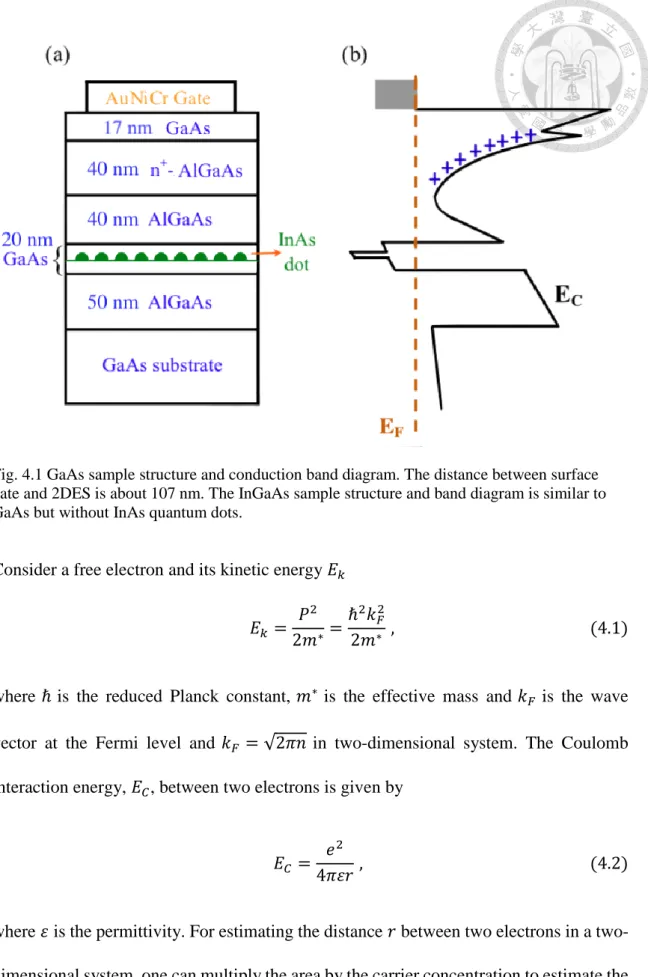
4.1 GaAs sample structure and conduction band diagram. The distance between surface gate and 2DES is about 107 nm. The InGaAs sample structure and band diagram is similar to GaAs but without InAs quantum dots. . . . . . 26 4.2 𝜌𝑥𝑥(𝐵) and 𝜌𝑥𝑦(𝐵) at 𝑉𝑔 = -0.274 V at various temperatures.. . . 31 4.3 The fitting result of equation (4.13) and one can use parameter B to determine
effective mass which is 0.162 𝑚0 where 𝑚0 is the rest mass of electron . . . 31 4.4 Upper figure is the 𝐵 − 𝜌𝑥𝑥 plot at 𝑉𝑔 = -0.284 V and the Δ𝜌𝑥𝑥 are 7.96 kΩ,
6.61 kΩ, 6.02 kΩ, 5.11 kΩ, 3.92 kΩ, 2.95 kΩ and 2.29 kΩ from temperature 0.01 K to 0.73 K respectively. The lower figure shows the result fitted by using SdH oscillations and the effective mass is 0.199 𝑚0 by using equation (4.14) . 32 4.5 Upper figure is the 𝐵 − 𝜌𝑥𝑥 plot at 𝑉𝑔 = -0.282 V and the Δ𝜌𝑥𝑥 are 6.58 kΩ,
5.49 kΩ, 4.78 kΩ, 4.06 kΩ, 3.38 kΩ, 2.52 kΩ, 2.04 kΩ from temperature 0.02 K to 0.74 K respectively. The lower figure shows the result fitted by using SdH oscillations and the effective mass is 0.194 𝑚0 by using equation (4.14) . . . 33 4.6 Upper figure is the 𝐵 − 𝜌𝑥𝑥 plot at 𝑉𝑔 = -0.280 V and the Δ𝜌𝑥𝑥 are 5.33 kΩ,
4.58 kΩ, 4.08 kΩ, 3.62 kΩ, 2.99 kΩ, 2.22 kΩ and 1.98 kΩ from temperature 0.03 K to 0.75 K respectively. The lower figure shows the result fitted by using SdH oscillations and the effective mass is 0.18 𝑚0 . . . 34 4.7 Upper figure is the 𝐵 − 𝜌𝑥𝑥 plot at 𝑉𝑔 = -0.276 V and the Δ𝜌𝑥𝑥 are 3.97 kΩ, 3.53 kΩ, 3.21 kΩ, 2.78 kΩ, 2.35 kΩ, 1.9 kΩ and 1.61 kΩ from temperature 0.05 K to 0.77 Krespectively. The lower figure shows the result fitted by using SdH oscillations and the effective mass is 0.169 𝑚0 . . . 35
4.8 Upper figure is the 𝐵 − 𝜌𝑥𝑥 plot at 𝑉𝑔 = -0.272 V and the Δ𝜌𝑥𝑥 are 3.01 kΩ, 2.85 kΩ, 2.5 kΩ, 2.2 kΩ, 1.98 kΩ, 1.67 kΩ and 1.4 kΩ from temperature 0.07 K to 0.79 K respectively. The lower figure shows the result fitted by using SdH oscillations and the effective mass is 0.154 𝑚0 . . . 36 4.9 Upper figure is the 𝐵 − 𝜌𝑥𝑥 plot at 𝑉𝑔 = -0.268 V and the Δ𝜌𝑥𝑥 are 2.34 kΩ, 2.27 kΩ, 2.02 kΩ, 1.75 kΩ, 1.67 kΩ, 1.42 kΩ and 1.26 kΩ from temperature 0.08 K to 0.80 K respectively. The lower figure shows the result fitted by using SdH oscillations and the effective mass is 0.14 𝑚0 . . . 37 4.10 Upper figure is the 𝐵 − 𝜌𝑥𝑥 plot at 𝑉𝑔 = -0.264 V and the Δ𝜌𝑥𝑥 are 1.8 kΩ, 1.81 kΩ, 1.68 kΩ, 1.55 kΩ, 1.43 kΩ, 1.29 kΩ and 1.15 kΩ from temperature 0.09 K o 0.81 K respectively. The lower figure shows the result fitted by using SdH oscillations and the effective mass is 0.12 𝑚0 . . . 38 4.11 Upper figure is the 𝐵 − 𝜌𝑥𝑥 plot at 𝑉𝑔 = -0.260 V and the Δ𝜌𝑥𝑥 are 1.53 kΩ, 1.49 kΩ, 1.40 kΩ, 1.32 kΩ, 1.34 kΩ, 1.22 kΩ and 1.1 kΩ from temperature 0.1 K to 0.82 K respectively. The lower figure shows the result fitted by using SdH oscillations and the effective mass is 0.099 𝑚0 . . . 39 4.12 Upper figure is the 𝐵 − 𝜌𝑥𝑥 plot at 𝑉𝑔 = -0.256 V and the Δ𝜌𝑥𝑥 are 1.29 kΩ, 1.3 kΩ, 1.27 kΩ, 1.2 kΩ, 1.16 kΩ and 1.17 kΩ from temperature 0.11 K to 0.71 K respectively. The lower figure shows the result fitted by using SdH oscillations and the effective mass is 0.074 𝑚0 . . . 40 4.13 Effective mass of GaAs changed by apply more negative gate voltage start from 0.074 𝑚0to 0.199𝑚0where 𝑚0 is the rest mass of electron . . . 41
4.15 Interaction strength 𝑟𝑠 become higher with apply more negative 𝑉𝑔 . . . 43 4.16 Relation between normalized effective mass 𝑚∗⁄ and interaction strength 𝑟𝑚 𝑠
where 𝑚∗ is the experimental result of effective mass of GaAs and 𝑚 is the ideal value of effective mass of GaAs . . . 44 4.17 The 𝐵 − 𝑅𝑥𝑥 plot and the Δ𝑅𝑥𝑥 at 𝐵 around 1.45T are 43.09 Ω, 42.62 Ω, 42.77 Ω, 42.16 Ω, 40.2 Ω, 39.08 Ω, 38.18 Ω, 37.32 Ω, 35.87 Ω, 35.04 Ω, 34.02 Ω, 33.18 Ω, 31.86 Ω, 30.44 Ω, 28.57 Ω and 26.64 Ω from temperature 0.1 K to 4.0 K respectively and the radio of width and length of the channel for deriving resistivity is 0.23 . . . 45 4.18 The result fitted by using SdH oscillations and the effective mass is 0.043 𝑚0 by using equation (4.14) . . . 45
1. Introduction of low-dimensional electron systems
1.1. Two-dimensional electron system
The two-dimensional electron system (2DES) has made a tremendous impact on modern condensed matter physics, materials science, and, to perhaps a lesser extent, statistical mechanics and quantum field theory. It lies at the boundary between three- dimensional electron systems, which are generally Fermi liquids, and one-dimensional systems, which are not. It also lies at another boundary which is between metals and insulators. The three-dimensional electron system in the presence of disorder (impurities and defects) can be an electrical conductor or insulator, but in the presence of any disorder, a one-dimensional system is always an insulator. Previously it was thought that the two-dimensional electron system was insulating [1], but recent experiments have shown that at low enough densities it can in fact be conducting [2]. In addition, it has a low electron density, which may be readily varied by means of an electric field. The low density implies a large Fermi wavelength (typically 10 nm), comparable to the dimensions of the smallest structures (nanostructures) that can be fabricated today. The electron mean free path can be quite large (exceeding 10 μm). Therefore, due to the combination of a large Fermi wavelength and large mean free path, quantum transport is conveniently studied in a 2DES.
1.1.1. The GaAs/Al
xGa
1-xAs heterostructure
In order to study quantum-mechanical effects in a 2DES, it is necessary to make a heterojunction using semiconductor materials that are as free from random unintentional potential modulation as possible. Because of the difference in their band gaps and to
electrons may form at the heterojunction interface. This accumulation layer is very thin (~ 100 Å ), such that the electron's motion in the direction perpendicular to the interface is quantized. The drawback with the metal-oxide-semiconductor junction is that there are occupied dopant states in the oxide-semiconductor interface region exactly where the two-dimensional system forms. In addition, the oxide barrier is not smooth and contains a high density of trapped charge since it is amorphous. The GaAs/AlxGa1-xAs heterostructure partly solves these problems: these heterostructures are grown by molecular beam epitaxy and the interface region where the 2DES forms is flat to within a monolayer with no trapped charge. Through the modulation doping, extremely high 2DES mobility can be obtained [3, 4].
The band structure of a GaAs/AlxGa1-xAs heterostructure in which a 2DES forms is shown in figure 1.1(a) before equilibration of the donor states. AlxGa1-xAs has a larger band gap than that of GaAs but has the same lattice structure, Al atoms substituting for Ga atoms, and approximately the same lattice constant. Electrons in the donor region in figure 1.1(a) are well above the bulk chemical potential and therefore flow out to the surface and interface regions during equilibration. As with the metal-oxide- semiconductor junction a dynamically 2DES can form at the interface, here at the GaAs/AlGaAs interface, if the doping concentration and length scales are chosen correctly. Figure 1.1(b) shows the result of equilibration, and the other sample of InAlAs/InGaAs also use the same concept to form 2DES at the interface.
Fig. 1.1 (a) GaAs/AlGaAs heterostructure before equilibration. (b) GaAs/AlGaAs heterostructure after equilibration. (Taken from Ref. [5])
1.1.2. Tuning the carrier concentration of a 2DES
The dependence of the carrier density 𝑛2𝐷 on surface gate voltage for both the metal-oxide-semiconductor junction and the GaAs/AlGaAs heterostructure may be calculated from a simple capacitor model. One plate of the capacitor is a metal surface gate and the other is the two-dimensional electron system. The capacitance of the device is approximately, 𝐶 = 𝜀𝐴/𝑑 where 𝑑 is the distance from the surface gate to the two- dimensional electron system and 𝐴 is the area of the device. If we substitute this into the capacitor equation 𝑄 = 𝐶𝑉𝑔 we have
𝑒Δ𝑛2𝐷𝐴 =𝜀𝐴
𝑑 Δ𝑉𝑔 , (1.1)
for an electron system, where Δ𝑛2𝐷 is the change in carrier density of the two- dimensional electron system caused by a change in gate voltage Δ𝑉𝑔, this simplifies to
Δ𝑛 = 𝜀
Δ𝑉 , (1.2)
it is the reason why we can adjust the two-dimensional electron density only by varying the applied gate voltage. By applying a negative bias to the metal surface, the height of the gate barrier is increased and the potential well at the GaAs/AlGaAs interface is reduced in energy. Eventually, the bound state in the potential minima is raised above the Fermi energy, depleting the well of free carriers. Conversely, by applying a positive bias to the gate, one may capacitively induce carriers into the 2DES [6].
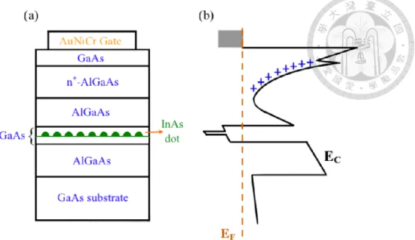
1.2. GaAs 2DES containing self-assembled InAs quantum dots
The fabrication of quantum dots has attracted a great deal of interest, both for investigating fundamental physics and device applications such as quantum dot solar cells [7], lasers [8], quantum computation [9], etc. Moreover, it has been discovered that dots can be self-assembled during a modified growth of highly lattice-mismatched semiconductors [10]. We note that, physicists have used InAs dots embedded in GaAs as a studied system which exhibits those behaviors [7-10].
The dots arise from this modified growth mechanism in which about 1 monolayer InAs uniformly covers the GaAs, which is called the wetting layer, but the subsequent InAs aggregates into three dimensional islands strained to the GaAs because of the about 7 % lattice mismatch between InAs and GaAs. Figure 1.2(a) shows the typical structure of the sample with a GaAs 2DES containing self-assembled InAs quantum dots. Figure 1.2(b) shows the schematic of the conduction band profile in the growth direction, at the site of InAs deposition.
Fig. 1.2 (a) Structure of the GaAs 2DES containing self-assembled InAs quantum dots sample.
(b) Schematic of the conduction band profile in the growth direction, at the site of InAs deposition.
When InAs self-assembled quantum dots are grown in the center of a GaAs/AlGaAs quantum well, the quantum dots provide the scattering for the 2DES. For example, in order to observe insulator-quantum Hall transition, Kim et al. showed that by depositing self-assembled InAs quantum dots in GaAs well as a short-range repulsive scattering site [11]. Sakaki et al. showed that by inducing InAs quantum dots in the vicinity (150-800 Å ) of a 2DES can dramatically reduce the transport mobility from 1.1×10⁵ to 1.1 ×103 cm2/V [12]. Moreover, Yoh et al. placed InAs quantum dots even closer to 2DES were able to measure some charging effects [13]. Therefore, it was shown how self-assembled InAs dots can tailor the electrical properties of 2DES. This provides new opportunities for controlled studies of the scattering of electrons in a 2DES. Here we used InAs self-assembled quantum dots growth in the region of a GaAs/AlGaAs heterostructure to study magnetoresistance oscillations in the strongly insulating regime as described in chapter 4.
References
1. Abrhams E, Anderson P W, Licciardello D C and Ramakrishnan T V 1979 Phys.
Rev. Lett. 42 763
2. Morán-López J L 2009 Fundamental of physics - Volume II
3. Stӧrmer H L, Dingle R, Gossard A C, Weigmann W and Sturge M D 1979 Solid State Commun. 29 705
4. Stӧrmer H L 1983 Surf. Sci. 132 519
5. Barnes C H W 2008 Quantum Electronics in Semiconductors 6. Kim G H, Ph.D. thesis 1998 Cambridge University
7. Nozik A J 2002 Physica E 14 115
8. Fafand S, Hinzer K, Raymond S, Dion M, McCaffrey J, Feng Y and Charbonnean S 1996 Science 274 1350
9. Fischer K A, Hanschke L, Wierzbowski J, Simmet T, Dory C, Finley J J, Vučković J and Müller K 2017 Nat. Phys. 13 649
10. Tsuchiya M, Gaines J M, Yan R H, Simes R J, Holtz P O, Coldren L A and Petroff P M 1989 Phys. Rev. Lett. 62, 466
11. Kim G H, Nicholls J T, Khondaker S I, Farrer I and Ritchie D A 2000 Phys. Rev. B 61 10910
12. Sakaki H, Yusa G, Someya T, Ohno Y, Noda T, Akiyama H, Kadoya Y and Noge H 1995 Appl. Phys. Lett. 67 3444
13. Yoh K, Konda J, Shiina S and Nishiguchi N 1997 Jpn. J. Appl. Phys. Part 1 36 4134
2. Transport theory in two-dimensional electron systems
2.1. Classical Hall effect
The significance of the Hall effect [1, 2] lies in determining the type and concentration of charge carriers which are two fundamental parameters for a semiconductor sample. This effect is easy to understand on the basis of the free-electron theory of a conductor. Let us consider a p-type semiconductor sample. When a magnetic field is present, these charges experience a force, called the Lorentz force. As illustrated in figure 2.1, a uniform magnetic field applied along the y-axis and a current I traverses the homogeneous sample along the x-direction. Thus, the Lorentz force
𝐹⃗ = 𝑞𝑣⃗ × 𝐵⃗⃗ = 𝑞𝑣𝑑𝐵𝑦𝑘̂ , (2.1)
where 𝑣𝑑 is the drift velocity of charge carrier, will deflect the trajectory of the carrier from its course. This mechanism leads to an accumulation of positive charges at the z-direction side of the sample. However, an electric field 𝐸𝐻 is inevitably produced toward the opposite z-direction to resist the Lorentz force. An equilibrium quickly develops in which the electric force on each positive charge builds up until it just cancels the Lorentz force. It means that when
𝑞𝐸𝐻= 𝑞𝑣𝑑𝐵𝑦 ⇒ 𝐸𝐻 = 𝑣𝑑𝐵𝑦 , (2.2)
the drifting carriers move along the specimen without further accumulation. A Hall potential difference 𝑉𝐻 is associated with the Hall field 𝐸𝐻 across sample width 𝑊 . The terminal voltage 𝑉𝐻= 𝐸𝐻𝑊 can be measured by connecting a voltmeter across the sample width. Furthermore, the drift velocity is related to the current density through
𝐽 = 𝑛𝑒𝑣𝑑 , (2.3)
where 𝑛 is the carrier concentration of the sample. This leads to
𝐸𝐻 = 1
𝑛𝑒𝐽𝐵𝑦 . (2.4)
The Hall field is thus proportional both to the current and to the magnetic field. In two dimensions, the proportionality constant 𝐸𝐻/𝐽𝐵𝑦 is known as the Hall coefficient, and is usually denoted by 𝑅𝐻= 1/𝑛𝑒 . Since 𝑅𝐻 is inversely proportional to the carrier concentration 𝑛, it follows that we can determine 𝑛 by measuring the Hall field. It is worth mentioning that the carrier concentration in a semiconductor may be different from the impurity concentration. In addition, the sign of the Hall coefficient depends on the sign of the charge carriers. Thus electrons and holes, being negatively and positively charged, lead to a negative and positive Hall coefficient respectively.
Fig. 2.1 A schematic diagram of the measurements of the classical Hall effect.
2.2. Density of states
The concept of density of states plays an important role in the study of electron transport properties. Density of states is the number of available electronic states per unit volume per unit energy around an energy 𝐸. For the free electron gas, the energy of the two-dimensional electrons in a single subband is given by
𝐸(𝑘⃗⃗) =ℏ2𝑘⃗⃗2
2𝑚∗ , (2.5)
where 𝑘⃗⃗ is the wave vector and 𝑚∗ is the effective mass of carrier. In a two-dimensional system, the k-space area between vector 𝑘⃗⃗ and 𝑘⃗⃗ + 𝑑𝑘⃗⃗ is 2𝜋𝑘𝑑𝑘. The k-space area per state is (2𝜋/𝐿)2. Therefore, the number of electron states in the region between 𝑘⃗⃗ and 𝑘⃗⃗ + 𝑑𝑘⃗⃗ are
2𝜋𝑘𝑑𝑘
4𝜋2 𝐿2 = 𝑘𝑑𝑘
2𝜋 𝐿2. (2.6)
Denoting the energy and energy interval corresponding to 𝑘⃗⃗ and 𝑑𝑘⃗⃗ as 𝐸 and 𝑑𝐸, we see that the number of electron states between 𝐸 and 𝐸 + 𝑑𝐸 per unit area are
𝑁(𝐸)𝑑𝐸 =𝑘𝑑𝑘
2𝜋 = 𝑚∗
2𝜋ℏ2𝑑𝐸 . (2.7)
Because electron can have two states for a given 𝑘-value: spin-up or spin-down, the density of states becomes
𝑁(𝐸) = 𝑚∗
𝜋ℏ2 . (2.8)
It is worth mentioning that in a 2DES the density of state shows no energy dependence.
Additionally, the ground state of electron is filled at zero temperature, we can obtain the relation
𝑛 = 𝑚∗
𝜋ℏ2𝐸𝐹 , (2.9)
where 𝑛 is the carrier density and 𝐸𝐹 is the Fermi energy. Using the above equation, the Fermi wave vectors (the radius of Fermi circle) is determined by
𝑘𝐹 =√2𝑚∗𝐸𝐹
ℏ = √2𝜋𝑛 . (2.10)
2.3. Landau quantization
The quantum Hall effect (QHE) was first discovered on condition that the degenerate electron gas in the inversion layer of a metal-oxide-semiconductor field-effect transistor is fully quantized when the transistor is operated in a strong magnetic field of order 15 T and at liquid helium temperatures [3]. The characteristic feature of quantum Hall effect is that the Hall resistance shows a serious of steps and precisely quantized Hall plateaus with applied magnetic field difference from the classical one which shows monotonic linear increasing resistance. It is impressive that the quantized Hall resistance 𝑅𝑥𝑦= ℎ/𝑣𝑒2, where ℎ is the Planck constant and 𝑣 is an integer filling factor, depends exclusively on fundamental constants and is not affected by irregularities in the semiconductor like impurities or interface effects. Normally, the energy E of mobile electrons in a semiconductor is quasi-continuous can be compared with the kinetic energy of free electrons with wave vector 𝑘 but with an effective mass 𝑚∗ ,
𝐸 = ℏ2
2𝑚∗(𝑘𝑥2+ 𝑘𝑦2+ 𝑘𝑧2) . (2.11)
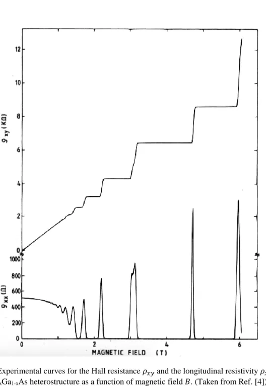
If the energy for motion in one direction (usually the z-direction) is fixed, one obtains a 2DES, and a strong magnetic field perpendicular to the two-dimensional plane will lead to a fully quantized energy spectrum, which is necessary for the observation of the QHE [4]. Figure 2.2 shows the typical QHE as a function of perpendicular magnetic field.
Fig. 2.2 Experimental curves for the Hall resistance 𝜌𝑥𝑦 and the longitudinal resistivity 𝜌𝑥𝑥 of a GaAs-AlxGa1-xAs heterostructure as a function of magnetic field 𝐵. (Taken from Ref. [4])
2.3.1. Landau levels
Here we will consider the conducting behavior of one electron in a two- dimensional plane with a strong perpendicular magnetic field applied. The Hamiltonian is given by
𝐻 = 1
2𝑚∗(𝑝⃗ − 𝑒𝐴⃗)2 , (2.12)
where 𝐴⃗ is the vector potential satisfies the condition 𝐵⃗⃗ = ∇⃗⃗⃗ × 𝐴⃗. To represent the Schrödinger equation 𝐻Ψ = 𝐸Ψ explicitly it is necessary to choose a gauge. Two particularly convenient gauges are the Landau gauge and the rotationally invariant symmetric gauge. The latter gauge is most useful in the study of interacting electrons [5].
So with suitable gauge transformation, the vector potential becomes 𝐴⃗ = (0, 𝐵𝑥, 0) , which gives a magnetic field in the z-direction 𝐵⃗⃗ = 𝐵𝑍̂. Then we can obtain the energy eigenvalues 𝐸𝑛 after solving the Schrödinger equation.
𝐸𝑛(𝑝𝑧, 𝑛) = 𝑝𝑧2
2𝑚∗+ (𝑛 +1
2) ℏ𝜔𝑐, 𝑛 = 0, 1, 2, 3, ⋯ , (2.13)
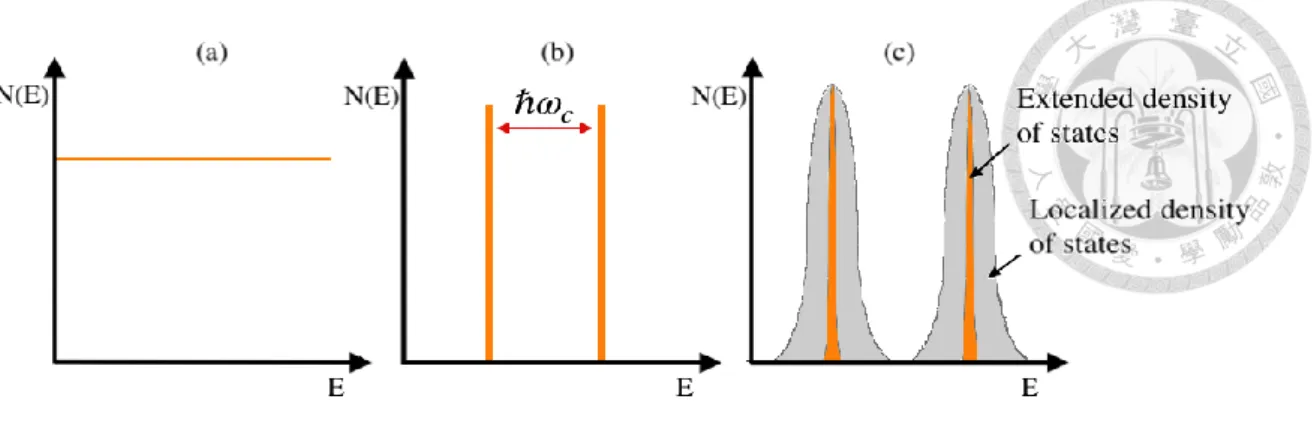
where 𝜔𝑐 = 𝑒𝐵/𝑚∗ is called cyclotron frequency. When in 2DES, the energy will be quantized into Landau levels, i.e. 𝐸𝑛 = (𝑛 + 1/2) ℏ𝜔𝑐 because of the confinement of electron to the x-y plane with 𝑝𝑧= 0. It is worth noting that the density of states of an unbound two-dimensional system is modified form the continuous band of states in zero magnetic field into the discrete energy levels, as shown in figure 2.3.
As shown in figure 2.3(b), in an ideal system, the density of states is like delta functions and the energy separation between the Landau levels is ℏ𝜔𝑐. However, in a real
Fig. 2.3 Schematic diagrams of density of state in a 2DES and 𝑁(𝐸) is density of state and 𝜔𝑐 = 𝑒𝐵/𝑚∗ is proportional to 𝐵. (a) At 𝐵 = 0, 𝑁 is constant. (b) At 𝐵 ≠ 0, 𝑁 is quantized by Landau quantization. (c) With the existence of disorder, Landau levels are broadened.
system, as shown in Fig 2.3(c) the Landau levels are broadened because of the existence of disorder.
2.3.2. Shubnikov-de Haas oscillations
The formation of Landau levels results in oscillations in the resistivity of a material essentially for the same reasons as discussed above. For measuring the effective mass of electron, these oscillations, known as Shubnikov-de Haas (SdH) effects has become a powerful tool to use in heterostructures and alloys.
At zero temperature and in the presence of a magnetic field the density of states 𝑔 acquires an oscillatory component Δ𝑔 which, at low fields, can be written [6]
Δ𝑔(𝜀)
𝑔0 = 2 ∑
𝑠=1
∞
exp(−𝑠𝜋/𝜔𝑐𝜏𝑞)cos (2𝑠𝜋𝜀
ℏ𝜔𝑐 − 𝑠𝜋) , (2.14)
where 𝑔0 is the zero-field density of states, 𝜔𝑐 = 𝑒𝐵/𝑚∗ is the cyclotron frequency, and 𝜀 is the electron energy. The above equation is valid subject to the Landau levels are broadened and each can be represented by a Lorentzian with a width Γ independent of energy or magnetic field, such that 𝜏𝑞 = ℏ/2Γ. When one gradually varies the magnetic
field perpendicular to the sample, the Fermi energy is swept by the alternate maxima and minima of density of states. These lead to a series of oscillations in the longitudinal resistivity, known as the SdH oscillations. Assuming only one subband is occupied and neglecting the contribution of higher harmonics, the oscillatory part Δ𝜌𝑥𝑥 of the magneto- resistivity can be expressed as [7]
Δ𝜌𝑥𝑥(𝐵, 𝑇) = 4𝜌0𝐷(𝑚∗, 𝑇)exp(− 𝜋
𝜇𝑞𝐵) , (2.15)
where 𝜌0 is a constant and expected to be the zero-filed longitudinal resistivity 𝜌𝑥𝑥(𝐵 = 0) although there are reports on the deviations [8], 𝜇𝑞 is the quantum mobility, the temperature factor 𝐷(𝑚∗, 𝑇) = 𝜒
𝑠𝑖𝑛ℎ𝜒, 𝜒 = 2𝜋2𝑘𝐵𝑚∗𝑇/ℏ𝑒𝐵, ℏ is the reduced Planck constant, 𝑘𝐵 is the Boltzmann constant, and 𝑚∗ is the electron effective mass. This equation is expected to hold true for small magneto-oscillations before well-developed quantum Hall states and zero longitudinal resistivity appear with increasing 𝐵 . This provide a useful tool for calculating effective mass 𝑚∗ and quantum lifetime 𝜏𝑞 from the temperature and magnetic field dependences of the SdH oscillations.
References
1. Huang K 1963 Statistical Mechanics, Wiley
2. Omar Ali M 1974 Elementary Solid State Physics, Addison-Wesley, Inc.
3. von Klitzing K, Dorda G and Pepper M 1980 Phys. Rev. Lett. 45 494
4. von Klitzing K 1986 Rev. Mod. Phys. 58 519
5. Prange R E and Girvin S M 1990 The Quantum Hall Effect, Springer-Verlag, Inc.
6. Isihara A and Smrčka L 1986 J. Phys. C 19 6777
7. Cho H-I, Gusev G M, Kvon Z D, Renard V T, Lee J-H and Portal J C 2005 Phys.
Rev. B 71 245323
8. Coleridge P T, Stoner R and Fletcher R 1989 Phys. Rev. B 39 1120
3. Device fabrication and experimental techniques
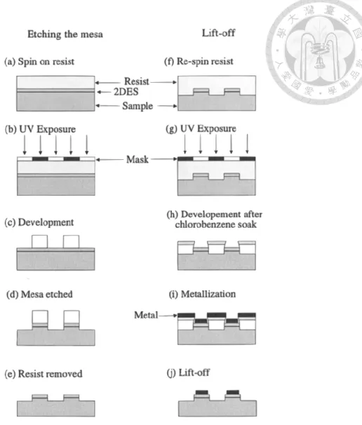
3.1. Device processing 3.1.1. Hall bar
Optical lithography is used to fabricate relative large structures like Hall bar, ohmic contact and gate pads [1]. Figure 3.1 shows the standard steps in the optical lithography processes. The cleaved chip is first immersed in dilute HCl solution to remove surface oxides. Mesa fabrication begins by spinning photoresist onto the surface of the cleaved chip. The chip is then backed for 10 minutes at 90°C in a fan oven to dry off any remaining solvent and harden the photoresist. A chrome-on-quartz glass photomask designed for a Hall bar is held above the sample to selectively expose the photoresist using ultra-violet light. The positive photoresist is broken into smaller organic units that are much more easily dissolved by developers that do not attack the unexposed material.
Therefore, the unexposed photoresist remaining on the surface of the chip will protect it from the subsequent wet-etch. The chip is then immersed in H2SO4 : H2O2 : H2O mixture, which etches the unprotected regions. The etching is allowed to proceed such that the underneath 2DES is completely destroyed, thereby electrically isolating the unetched regions. All resist is removed from the chips' surface by immersing the sample in acetone.
Accordingly, a Hall bar shaped mesa is left above the cleaved chip as shown in figure 3.1(a)~(e).
Fig. 3.1 A schematic diagram illustrating the optical lithography processing steps. (Taken from Ref. [1])
3.1.2. Ohmic contacts
An annealed AuGeNi metallization is the most common technique used to fabricate conventional ohmic contacts to a 2DES. The chip is soaked in chlorobenzene to harden the top surface of the photoresist after exposure through a second photomask. The hardened surface of the resist develops at a slower rate than the lower layers and an overhang edge profile is produced. This is necessary for easy lift-off of the subsequent metallization stages [1]. In order to improve the adhesion of the ohmic metallization, dipped the sample in a dilute HCl solution to remove the oxide layer from surface. The
AuGeNi are evaporated onto the surface of the sample in the required thickness. After the evaporation, used the acetone to remove the metal deposited on it and the remaining resist, leaving the metal lying directly in contact with the surface of the sample.
Subsequently the evaporated metal was annealed such that the metal diffused down through the chip and contacts the 2DES. This is the procedure for fabricating ohmic contacts as illustrated in figure 3.1(f)~(j). The quality of the contacts is examined by linear I-V characteristics both at room temperature and at 77 K to check whether the contact is
good or not to the 2DES. It is quite common for contacts to freeze-out at low temperatures. If this is the case, the chip may be re-annealed to improve poor contacts.
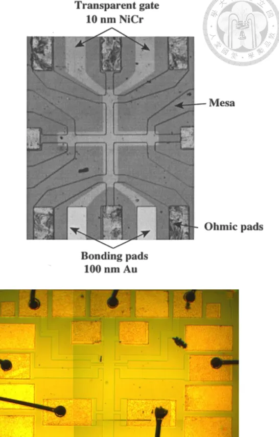
3.1.3. Front gate
The procedure for depositing a front gate is similar to depositing the ohmic contact metallization but without the annealing stage. For better adhering to the GaAs surface, the gate metallization used a 10 nm layer of NiCr. In order to make electrical contact to the NiCr gate, a 100 nm Au layer is evaporated to create bond pads (see figure 3.2). The completed Hall bar is shown in figure 3.2.
Fig. 3.2 An optical photograph (50 × magnification) of a completed Hall bar of GaAs with
3.2. Cryogenic system
An Oxford Instruments dilution refrigerator can perform measurement at temperatures from 600 mK to 20 mK and magnetic fields up to 13.6 T. A device is mounted on a probe and gently lowered into the 3He space. Base temperature is reached in about 2-3 hours after fully insert the sample. When the mixture of liquid 3He and 4He is cooled below a tri-critical point (about 869 mK, see figure 3.3), it separates into two phases: One phase contains more 3He, so called the concentrated phase. The other contains less 3He, so called the dilute phase (6% 3He in 94% 4He). The cooling mechanism is obtained from the evaporating of 3He from the concentrated phase into the dilute phase and 3He which are removed from the dilute phase are recondensed into liquid 3He at the still.
The pumping system at room temperature then return 3He to concentrated phase by removing the 3He gas from the still and passes it through the nitrogen and helium cold trap to remove impurities. And the 3He is condensed by passing it through a tube in thermal contact with the helium main bath and condensing on the 1 K pot. A flow impedance is used to maintain a high enough pressure in the 1 K pot region for the gas to condense whilst allowing a flow pass through at a reduced pressure. After passing through the heat exchanger, the liquid 3He enter the condensed phase. This circulation of 3He allows the base temperature to be maintained indefinitely.
Fig. 3.3 Phase diagram of 3He-4He mixtures.
3.3. Measurement set-up
3.3.1. Four-terminal resistance measurement
The four-terminal resistance measurement is the normal technique for the transport measurement without the influence of contact resistance. The technique is based on the van der Pauw method, and the following conditions need to be satisfied:
1. The sample must have a flat shape of uniform thickness.
2. The sample must not have any isolated holes.
3. The sample must be homogeneous and isotropic.
4. All four contacts must be located at the edges of the sample.
5. The contacts are sufficiently small.
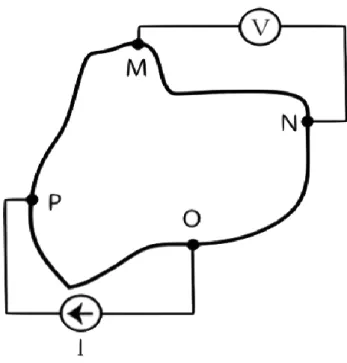
Fig. 3.5 A schematic diagram of van der Pauw electrical configuration with contacts on the boundary of the sample. (Taken from Ref. [2])
Figure 3.5 shows an arbitrarily shaped sample with four contacts at the edges. Base on the theoretical result deduced by van der Pauw in 1958 [2]:
exp{−𝜋𝑑
𝜌 𝑅𝑀𝑁,𝑂𝑃} + exp{−𝜋𝑑
𝜌 𝑅𝑁𝑂,𝑃𝑀} = 1 , (3.1)
where 𝜌 is the resistivity and 𝑑 is the thickness of the sample and the definition of resistance 𝑅𝑀𝑁,𝑂𝑃 is
𝑅𝑀𝑁,𝑂𝑃 ≡ 𝑉𝑀𝑁
𝐼𝑂𝑃 , (3.2)
where 𝑉𝑀𝑁 is the potential difference between contact 𝑀 and 𝑁 when a current 𝐼𝑂𝑃 is passed through contact 𝑂 and 𝑃. We can derive the resistivity of the sample from the equation above by numerical method after the measurement.
In the measurement, the standard four-terminal AC lock-in techniques were used on the sample with Hall bar shape as shown in figure 3.6. The longitudinal resistance can be defined as 𝑅𝑥𝑥 = 𝑉34/𝐼, and Hall resistance can be defined as 𝑅𝑥𝑦= 𝑉24/𝐼.
References
1. Kim G H, Ph.D. thesis 1998 Cambridge University
2. Lim S H N, McKenzie D R and Bilek M M M 2009 Rev. Sci. Instrum. 80 075109
4. Magnetoresistance oscillations in GaAs and InGaAs systems
4.1. Introduction
This chapter discusses magnetoresistance measurements performed on GaAs/
AlGaAs and InGaAs/InAlAs heterostructures. The former one contains self-assembled InAs dots which have been inserted in the center of the GaAs quantum well. The data was taken by Gil-Ho Kim and detailed analysis in the strongly insulating regime was done by me. The latter one is measured by me and other group members and detailed analysis was also done by me. As mentioned in section 2.3.2, here we use the SdH oscillations to determine the effective mass of GaAs and InGaAs. Since we can tune the GaAs sample’s effective disorder of this 2DES by changing the bias, we have obtained the relation between disorder and effective mass and will discuss it later.
4.2. Device structure
The structure and conduction band diagram of GaAs sample are schematically shown in figure 4.1. The self-assembled InAs quantum dots serve as scattering centers for the 2DES.
4.3. Background
4.3.1. The radio of Coulomb energy to kinetic energy 𝑟
𝑠Here we define a symbol 𝑟𝑠 as the radio of Coulomb energy to kinetic energy to compare how large is the disorder interaction in 2DES.
Fig. 4.1 GaAs sample structure and conduction band diagram. The distance between surface gate and 2DES is about 107 nm. The InGaAs sample structure and band diagram is similar to GaAs but without InAs quantum dots.
Consider a free electron and its kinetic energy 𝐸𝑘
𝐸𝑘 = 𝑃2
2𝑚∗ =ℏ2𝑘𝐹2
2𝑚∗ , (4.1)
where ℏ is the reduced Planck constant, 𝑚∗ is the effective mass and 𝑘𝐹 is the wave vector at the Fermi level and 𝑘𝐹 = √2𝜋𝑛 in two-dimensional system. The Coulomb interaction energy, 𝐸𝐶, between two electrons is given by
𝐸𝐶 = 𝑒2
4𝜋𝜀𝑟 , (4.2)
where 𝜀 is the permittivity. For estimating the distance 𝑟 between two electrons in a two- dimensional system, one can multiply the area by the carrier concentration to estimate the average distance between two electrons
(𝜋𝑟2)𝑛 = 1 ⇒ 𝑟 = 1
√𝜋𝑛 . (4.3)
From the equation above, we obtain
𝑟𝑠 = 𝐸𝐶 𝐸𝑘 =
𝑒2 4𝜋𝜀 1
√𝜋𝑛 ℏ2𝑘𝐹2
2𝑚∗
= 𝑒2 4𝜋𝜀 1
√𝜋𝑛 ℏ2(2𝜋𝑛)
2𝑚∗
= 𝑚∗𝑒2
4𝜋𝜀ℏ2√𝜋𝑛∝𝑚∗
√𝑛 , (4.4)
since we can tune the carrier density by varying the bias, the effective disorder will change together and the effective mass may change, too. That is the reason we cannot treat the effective mass as a constant in this 2DES. In later analysis of the experiment data, by using the SdH oscillations, we will show that the effective mass does change with bias.
4.3.2. Effective mass
The electrons in crystal are not free, but instead interact with the periodic potential of the lattice. The movement of electrons in periodic potential over long distances larger than the lattice spacing, can be very different from their motion in vacuum. The canonical definition given for the effective mass is that it is related to the curvature of the conduction and valence bands in the band structure (energy dispersion in terms of k-vector) for electrons and holes respectively. We can see that from the following: the definition of group velocity 𝑣𝑔 = 𝑑𝜔/𝑑𝑘 and the frequency associated with a wave function of energy 𝜖 by quantum theory is 𝜔 = 𝜖/ℏ, and so
𝑣𝑔 =1 ℏ
𝑑𝜖
𝑑𝑘 , (4.5)
and then differential the above group velocity to obtain
𝑑𝑣𝑔 𝑑𝑡 =1
ℏ 𝑑2𝜖 𝑑𝑘𝑑𝑡= 1
ℏ(𝑑2𝜖 𝑑𝑘2
𝑑𝑘
𝑑𝑡) . (4.6) The work 𝛿𝜖 done on the electron by the electric field 𝐸 in the time interval 𝛿𝑡 is
𝛿𝜖 = −𝑒𝐸𝑣𝑔𝛿𝑡 , (4.7)
and by using (4.5) we observe that
𝛿𝜖 = 𝑑𝜖
𝑑𝑘𝛿𝑘 = ℏ𝑣𝑔𝛿𝑘 , (4.8)
on comparing (4.6) with (4.7) we have
𝛿𝑘 = −(𝑒𝐸
ℏ)𝛿𝑡 , (4.9)
where ℏ𝑑𝑘/𝑑𝑡 = −𝑒𝐸. So we can write (4.9) in terms of the external force 𝐹⃗ as
ℏ𝑑𝑘⃗⃗
𝑑𝑡 = 𝐹⃗ . (4.10)
According to (4.10), (4.6) becomes
𝑑𝑣𝑔 𝑑𝑡 = (1
ℏ2 𝑑2𝜖
𝑑𝑘2)𝐹 . (4.11)
If we identify ℏ2/(𝑑2𝜖/𝑑𝑘2) as a mass, then (4.11) assumes the form of Newton’s second law and define the effective mass 𝑚∗ by
1 𝑚∗ = 1
ℏ2 𝑑2𝜖
𝑑𝑘2 , (4.12)
and that is the canonical definition of effective mass. But with the help of SdH oscillations, we can get the effective mass as well which I will introduce in section 4.5.
4.3.3. Insulator-quantum Hall transition
Insulator-quantum Hall (I-QH) transition is an interesting physical phenomenon in the field of two-dimensional physics and is predicted by Kivelson, Lee and Zhang [1]
in their seminal work on the global phase diagram (GPD). It is worth mentioning that the scattering introduced by the self-assembled InAs quantum dots provides the necessary disorder to observe I-QH transitions. It is possible to manipulate the screened random potential experienced by the electrons by varying their density. From section 1.1.2 we know that by varying the gate voltage 𝑉𝑔, the carrier density 𝑛 can be varied therefore 𝑉𝑔 can be regarded as a means of varying the effective disorder of the sample, an important parameter in the study of I-QH transition [2]. The temperature-independent points in 𝜌𝑥𝑥 at a critical magnetic field BC are the signature of I-QH transition.
For B < BC, 𝜌𝑥𝑥 decreases with increasing temperature, characteristics of an insulating regime and for B > BC, 𝜌𝑥𝑥 increasing with increasing temperature, which shows that the 2DES is in quantum Hall regime. Within the GPD, the only allowed I-QH transition is the spin-degenerate 0-2 transition where the symbols 0 and 2 correspond to the insulating state and the 𝜈 = 2 QH state, respectively [1].
In most cases, before a strongly-disordered 2D system enters the I-QH transition, no oscillations in 𝜌𝑥𝑥 can be observed in the insulating state. However, in our GaAs 2DES containing self-assembled InAs quantum dots, pronounced oscillations in 𝜌𝑥𝑥 can be observed. Such features provide compelling experimental evidence for Landau quantization in the insulating state. As a result, we intend to further probe these interesting oscillations in the insulating state.
4.4. Result and discussion 4.4.1. GaAs Sample
This section shows how we calculate the effective mass of GaAs sample by using the observed SdH oscillations. Figure 4.2 presents one of the experimental results for showing the procedure of determining the effective mass. According to section 2.3.2, we calculate Δ𝜌𝑥𝑥(𝐵, 𝑇), the amplitude of SdH oscillations, first by connecting the inflection point around filling factor 𝜈 = 4 and find the difference between the dashed lines at 𝜈 = 4 to the lowest point of corresponding curve (with same color) and then divided by 2 which are 3.41 kΩ, 3.17 kΩ, 2.9 kΩ, 2.48 kΩ, 2.16 kΩ, 1.73 kΩ and 1.49 kΩ from 0.06 K to 0.78 K respectively. When this method is applied, one usually chooses 𝜈 much greater than we do to avoid appearance of spin splitting and quantum Hall state but in this paper, they determine the effective mass with 𝜈 → 1/2 [3]. On the other hand, based on the experimental result, 𝜈 = 4 is the suitable choice we get to calculate Δ𝜌𝑥𝑥(𝐵, 𝑇).
The temperature-independent points in 𝜌𝑥𝑥 at BC1 ≈ 1.2 T and BC2 ≈ 2.1 T and this transition is referred to as 0-2-0. Based on the GPD, the only allowed I-QH transition is the spin-degenerate 0-2 transition therefore the oscillation we use to calculate Δ𝜌𝑥𝑥 is 𝜈 = 4 (as we can see in the measured Hall resistance xy).
To fit the Δ𝜌𝑥𝑥 with equation (2.15), we first rewrite the equation to this form
Δ𝜌𝑥𝑥(𝐵, 𝑇) = 4𝜌0𝐷(𝑚∗, 𝑇)exp(− 𝜋
𝜇𝑞𝐵) ⇒ (2.15) Δ𝜌𝑥𝑥 ≡ 𝑦(𝑇) = αβ𝑇
sinh(β𝑇), α = 4𝜌0exp (− 𝜋
𝜇𝑞𝐵) , β =2𝜋2𝑘𝐵𝑚∗
ℏ𝑒𝐵 , (4.13)
where 𝜌0 is a constant and expected to be the zero-filed longitudinal resistivity, 𝜇𝑞 is the quantum mobility, the temperature factor 𝐷(𝑚∗, 𝑇) = 𝜒
𝑠𝑖𝑛ℎ𝜒, 𝜒 = 2𝜋2𝑘𝐵𝑚∗𝑇/ℏ𝑒𝐵 , ℏ is the reduced Planck constant, 𝑘𝐵 is the Boltzmann constant and 𝑚∗ is the electron effective mass. From equation (4.13) we can now determine the effective mass.
𝑚∗ = β ∙ ℏ𝑒𝐵
2𝜋2𝑘𝐵 . (4.14)
0.0 0.5 1.0 1.5 2.0 2.5
0 20 40 60
BC2
0.42 K 0.54 K 0.66 K 0.78 K 0.06 K 0.18 K 0.30 K 0.42 K 0.54 K 0.66 K 0.78 K
xx& xy (k)
B (T)
Vg = -0.274 V
BC1
Fig. 4.2 𝜌𝑥𝑥(𝐵) and 𝜌𝑥𝑦(𝐵) at 𝑉𝑔 = -0.274 V at various temperatures.
0.0 0.1 0.2 0.3 0.4 0.5 0.6 0.7 0.8
2 3
Δxx SdH fit of Δxx
Δxx (kΩ)
T (K)
Model sdH (User)
Equation α * β * x / sinh(β * x) Reduced
Chi-Sqr
0.0035
Adj. R-Squar 0.99336
Value Standard Erro
△ ρxx α 3.37032 0.03995
β 3.17321 0.06701
The following figures are the rest of experiment data of 𝐵 − 𝜌𝑥𝑥 plot and its 𝑇 − Δ𝜌𝑥𝑥 plot start from gate voltage 𝑉𝑔 = −0.284 V to 𝑉𝑔 = −0.256 V.
0.0 0.2 0.4 0.6 0.8 1.0 1.2 1.4 1.6 1.8 2.0 0
20 40 60 80 100 120
0.01 K 0.13 K 0.25 K 0.37 K 0.49 K 0.61 K 0.73 K
xx (kΩ)
B (T) Vg = -0.284 V
0.0 0.1 0.2 0.3 0.4 0.5 0.6 0.7
2 3 4 5 6 7 8
Δxx
SdH fit of Δxx
Δ xx (kΩ)
T (K)
Model sdH (User)
Equation α * β * x / sinh(β * x) Reduced
Chi-Sqr
0.11184
Adj. R-Square 0.97327
Value Standard Error
△ ρxx α 7.41814 0.2239
β 4.2096 0.20113
Fig. 4.4 Upper figure is the 𝐵 − 𝜌𝑥𝑥 plot at 𝑉𝑔 = -0.284 V and the Δ𝜌𝑥𝑥 are 7.96 kΩ, 6.61 kΩ, 6.02 kΩ, 5.11 kΩ, 3.92 kΩ, 2.95 kΩ and 2.29 kΩ from temperature 0.01 K to 0.73 K
respectively. The lower figure shows the result fitted by using SdH oscillations and the effective mass is 0.199 𝑚0 by using equation (4.14).
0.0 0.5 1.0 1.5 2.0 0
20 40 60 80 100 120
0.02 K 0.14 K 0.26 K 0.38 K 0.50 K 0.62 K 0.74 K
xx (k)
B (T) Vg = -0.282 V
0.0 0.1 0.2 0.3 0.4 0.5 0.6 0.7
2 4 6
Δxx
SdH fit of Δxx
Δ xx (kΩ)
T (K)
Model sdH (User)
Equation α * β * x / sinh(β * x) Reduced
Chi-Sqr
0.10043
Adj. R-Square 0.96187
Value Standard Erro
△ ρxx α 6.08012 0.21347
β 4.04656 0.22598
Fig. 4.5 Upper figure is the 𝐵 − 𝜌𝑥𝑥 plot at 𝑉𝑔 = -0.282 V and the Δ𝜌𝑥𝑥 are 6.58 kΩ, 5.49 kΩ, 4.78 kΩ, 4.06 kΩ, 3.38 kΩ, 2.52 kΩ and 2.04 kΩ from temperature 0.02 K to 0.74 K
respectively. The lower figure shows the result fitted by using SdH oscillations and the effective mass is 0.194 𝑚0 by using equation (4.14).
0.5 1.0 1.5 2.0 0
20 40 60 80 100 120
xx (k)
0.03 K 0.15 K 0.27 K 0.39 K 0.51 K 0.63 K 0.75 K
B (T) Vg = -0.280 V
0.0 0.1 0.2 0.3 0.4 0.5 0.6 0.7
2.0 2.5 3.0 3.5 4.0 4.5 5.0 5.5
Δxx
SdH fit of Δxx
Δ xx (kΩ)
T (K)
Model sdH (User)
Equation α * β * x / sinh(β * x) Reduced
Chi-Sqr
0.04704
Adj. R-Square 0.96884
Value Standard Erro
△ ρxx α 5.01204 0.14467
β 3.66392 0.17703
Fig. 4.6 Upper figure is the 𝐵 − 𝜌𝑥𝑥 plot at 𝑉𝑔 = -0.280 V and the Δ𝜌𝑥𝑥 are 5.33 kΩ, 4.58 kΩ, 4.08 kΩ, 3.62 kΩ, 2.99 kΩ, 2.22 kΩ and 1.98 kΩ from temperature 0.03 K to 0.75 K respectively.
The lower figure shows the result fitted by using SdH oscillations and the effective mass is 0.18 𝑚0.
0.5 1.0 1.5 2.0 0
20 40 60 80
Vg = -0.276 V 0.05 K
0.17 K 0.29 K 0.41 K 0.53 K 0.65 K 0.77 K
xx (k)
B (T)
0.0 0.1 0.2 0.3 0.4 0.5 0.6 0.7 0.8
1.5 2.0 2.5 3.0 3.5 4.0
Δxx
SdH fit of Δxx
Δ xx (kΩ)
T (K)
Model sdH (User)
Equation α * β * x / sinh(β * x) Reduced
Chi-Sqr
0.0115
Adj. R-Square 0.98461
Value Standard Erro
△ ρxx α 3.82249 0.0722
β 3.34673 0.10949
Fig. 4.7 Upper figure is the 𝐵 − 𝜌𝑥𝑥 plot at 𝑉𝑔 = -0.276 V and the Δ𝜌𝑥𝑥 are 3.97 kΩ, 3.53 kΩ, 3.21 kΩ, 2.78 kΩ, 2.35 kΩ, 1.9 kΩ and 1.61 kΩ from temperature 0.05 K to 0.77 K respectively.
The lower figure shows the result fitted by using SdH oscillations and the effective mass is


![Figure 3.5 shows an arbitrarily shaped sample with four contacts at the edges. Base on the theoretical result deduced by van der Pauw in 1958 [2]:](https://thumb-ap.123doks.com/thumbv2/9libinfo/9608689.634196/34.892.179.780.97.1131/figure-arbitrarily-shaped-sample-contacts-theoretical-result-deduced.webp)