國立臺灣大學電機資訊學院光電工程學研究所 碩士論文
Graduate Institute of Electro-Optical Engineering College of Electrical Engineering & Computer Science
National Taiwan University Master Thesis
製作抗反射與低滑落角的 次波長複層結構於矽基板上
Fabrication of subwavelength dual structures on silicon substrates with anti-reflection and low sliding angles
江杰修
Chiao-Hsiu Chiang
指導教授:王 倫 博士 Advisor: Lon A. Wang, Ph. D
中華民國 99 年 7 月 July, 2010
致謝
本篇論文能夠順利完成,首先要感謝的是王倫教授的指導,再來 就是家人朋友的支持,以及實驗室夥伴們的協助,感謝永彬、哲豪、
智昇、子軒關於實驗上的指導,冠宇、信傑同儕間共患難的革命情感,
以及學弟治賢、慶東在實驗上的協助,還有明遠、家翔、榮春、瑞禎 在實驗以及行政上的幫助。
很感謝台積電的張先生提供我們光阻,還有張所鈜教授提供我們
AFM。
最後也許還有我沒有想到但是曾經幫助過我的人,在這裡我也衷 心感謝。
摘要
在各式各樣的光學應用中,例如在太陽能電池上的抗反射結構,
自清潔功能也成了一個潛在需要的性質。而自清潔功能與小的滑落角 息息相關。
從先前的文獻中我們發現同時擁有抗反射與較小滑落角的奈米 結構已經被製作出來了,然而在文獻中此種擁有兩種特性的結構通常 具有高深寬比。蟬翅上的奈米結構被發現可同時擁有此兩種特性,深 寬比較低,並且某部份的這種結構屬於複層的結構。於是我們提出一 個新的製程方法來製作這樣的結構。利用干涉微影及乾蝕刻的技術,
我們製作出奈米複層結構,並且我們利用自行組裝的反射儀、接觸角 量測儀跟滑落角量測儀來量測此種複層結構的反射率、接觸角及滑落 角。
關鍵字:干涉微影、 抗反射、疏水性
Abstract
For various optical applications such as anti-reflection surfaces on solar cells, self-cleaning property is potentially required. The self-cleaning property is related to low sliding angle.
From previously published paper, some kinds of nano structures were fabricated to have anti-reflection and low sliding angle. However, these structures which possess both properties usually had high aspect ratios.
It was found that the nano structure on the surface of cicada wing possessed both properties simultaneously and has low aspect ratio. Some of the structures were found to be dual structures. We introduce a new method to fabricate this kind of dual structure. By using two-beam interference lithography and dry etching processes, the nano dual structures have been fabricated. The reflectance, contact angle, and sliding angle of the nano dual structures were measured by our home made reflectometer, contact angle analyzer, and sliding angle analyzer.
Keywords:Two-beam interference lithography, anti-reflection and hydrophobicity
Statement of Contributions
General Contributions
The following are substantial items although not my original contributions.
1. Uniformity improvement of film thickness over a 4” silicon wafer.
2. Setup for contact angle and sliding angle measurement.
Contents
致謝 ... I 摘要 ... II Abstract ... III Statement of Contributions ... IV
Contents ... 1
List of Figures ... 3
Chapter 1. Introduction ... 6
1-1 Background and Motivation... 6
1-1-1 Wettability of a Solid Surface ... 10
1-1-2 Anti-Reflective Nano Structure ... 15
1-1-3 Hydrophobic and Anti-Reflective Nano Structure ... 20
1-2 Organization of the Thesis ... 27
Chapter 2. Design and Simulation ... 28
2-1 Grating Equation, TFT and EMT ... 28
2-2 Simulated Reflectance of Bell-shaped Structure, Cone structure, and Dual Structure by Using RCWA ... 33
2-3 Summary ... 38
Chapter 3. Fabrication ... 39
3-1 ARC and PR Coating ... 41
3-2 Two-beam Interference Lithography ... 48
3-2-1 Exposure Principle of Two-beam Interference Lithography ... 48
3-2-2 Exposure and Development ... 48
3-3 Pattern Transfer to ARC and Silicon Dioxide by RIE ... 55
3-4 Pattern Transfer from ARC and Silicon Dioxide Pattern to Silicon Substrate by ICP-RIE ... 59
3-5 Tunable Ratio of the Heights between Upper Part and Lower Part of the Structure ... 66
3-6 Surface Modification ... 69
3-7 Summary ... 70
Chapter 4. Measurement ... 71
4-1 Measurement of Contact Angle and Sliding Angle ... 71
4-2 Measurement of Reflectance ... 78
Chapter 5. Conclusion and Future Work ... 85
5-1 Conclusion ... 85
5-2 Future Work... 86 References ... 87
List of Figures
Fig. 1-1 An SEM image of a lotus leaf shows the two-scale roughness [1].. 7 Fig. 1-2 Images of the non-wetting leg of a water strider. (a) A water droplet on a leg with a contact angle of 167.6o±4.4o; (b) and (c), SEM images of the leg show numerous oriented spindly microsetae (b) and the fine nano scale grooved structures on a seta (c). Scale bars: (b) 20 mm, (c) 200 nm [2]... 8 Fig. 1-3 An SEM image of a cicada wing [3]. ... 9 Fig. 1-4 (a) Wenzel state [4], (b) Cassie-Baxter state [5]. ... 12 Fig. 1-5 (a, b) Field emission SEM images of the cobalt hydroxide films
observed from the top and side, respectively. (c) TEM images of the cobalt hydroxide films. (d) A simple model of the film with the fractal structure [6]. ... 13 Fig. 1-6 Measured reflectance spectrum and simulated reflectance spectra
by using RCWA and TFT models [11]. The SEM image of the structure is shown in the upper-left corner of the figure. ... 17 Fig. 1-7 (a) Inverted pyramid structure on a silicon substrate
(b)Experimental (solid) and RCWA-simulated (dotted) specular optical reflectivity at normal incidence. Black: bare (100) silicon wafer. Red:
360 nm size pyramids template from 320 nm silica spheres [15]. ... 19 Fig. 1-8 Inverted pyramid arrays on a silicon substrate [16]. ... 21 Fig. 1-9 Silicon nanopillar array fabricated by nano particles and reactive
ion etching [17]. ... 22 Fig. 1-10 High aspect ratio hollow-tip array on silicon substrate [18]. ... 24 Fig. 1-11 TEM image of the hollow-tip detached from the substrate [18]. 24 Fig. 1-12 A general shape of dual structure. The aspect ratio of top part is
defined by w1/h1. The aspect ratio of the total structure is defined by w2/h2. ... 26 Fig. 2-1 Reflective light of higher order appears when the period of the
grating is larger than the wavelength. ... 29 Fig. 2-2 Only reflective light of zero order appears when the period of the
grating is smaller than the wavelength of incident light and the angle of incident light is not large. ... 30 Fig. 2-3 Subwavelength structure is divided into nine layers. ... 32 Fig. 2-4 General structure for simulation. ... 34 Fig. 2-5 (a) Structure shapes for simulation (b) Average reflectance of dual
structures, cones array, and bell-shaped structures array corresponding
to different structure heights. ... 37
Fig. 3-1 Processing steps. ... 40
Fig. 3-2 Reflectance in the interface between PR and ARC layers. ... 43
Fig. 3-3 Spin speed curve of ARC [20]. ... 44
Fig. 3-4 Spin speed curve of PR [21]. ... 46
Fig. 3-5 Exposure system of two-beam interference lithography. ... 49
Fig. 3-6 Two-beam interference image with higher exposure dosage. ... 51
Fig. 3-7 Two-beam interference image with lower exposure dosage. ... 51
Fig. 3-8 SEM image: PR pattern of posts array (total exposure dosage: 58mJ). ... 52
Fig. 3-9 SEM image: PR pattern of holes array (total exposure dosage: 42mJ). ... 52
Fig. 3-10 SEM image: side view of PR pattern of posts array. ... 54
Fig. 3-11 AFM image of ARC and silicon dioxide pattern. ... 58
Fig. 3-12 ICP system located in the Institute of Physics, Academia Sinica. 61 Fig. 3-13 The influence of passivation time on profile control. Passivation time:(a) 6s (b) 7.5s (c) 9s. ... 62
Fig. 3-14 The influence of oxygen flow rate on profile control. Oxygen flow rate:(a) 0sccm (b) 2sccm (c) 7sccm. ... 63
Fig. 3-15 Dual structure A. ... 64
Fig. 3-16 Dual structure B. ... 64
Fig. 3-17 Dual structure C. ... 65
Fig. 3-18 Dual structure D. ... 67
Fig. 3-19 Dual structure E. ... 67
Fig. 4-1 Contact angle analyzer. ... 73
Fig. 4-2 Setup for sliding angle measurement for <5o. ... 74
Fig. 4-3 Setup for sliding angle measurement (a) First calibration (b) Then sliding angle measurement. ... 74
Fig. 4-4 Setup for sliding angle measurement >5o ... 75
Fig. 4-5 Dual structure A, B, C, D, and E. ... 76
Fig. 4-6 Simple structures. ... 77
Fig. 4-7 Setup for reflectance measurement. ... 80
Fig. 4-8 Measured reflectance spectra of 5 dual structures and flat silicon. 81 Fig. 4-9 (a) Dual structure B (b) Reflectance spectra of dual structure B and simulated SWSs. The shapes shown in the up-left corner were used for simulation and the structure height for simulation is 540 nm. The 3 shapes were described by Eq. (2.3) and v was 4 here. ... 82
Fig. 4-10 (a) Structure shapes for simulation and the structure height is set to 405 nm (b) Dual structure C (c) Simulated reflectance spectra of Fig.
4-10 (a) and flat silicon and measured reflectance of dual structure C.
... 83
Chapter 1. Introduction
1-1 Background and Motivation
Naturally occurring structures is a rich source of products that meets specific functions which are imposed by natural selection. The surface relief structure of animals and plants is one of the most attractive topics. Many papers have revealed lots of micro and nano structures on the surface of creatures. Some kinds of these structures were observed complex. A lotus leaf, the most famous superhydrophobic example, was observed by W. Barthlott et al. in 1997 [1]. As shown in Fig. 1-1, the microscopic SEM image of a lotus leaf showed the two-scale roughness, dots on a dot array. The water contact angle of a lotus leaf is 161 o. Legs of a water strider, another famous superhydrophobic example, were observed by X. F. Gao et el. in 2004 [2]. As shown in Fig. 1-2, the leg of a water strider also shows two-scale roughness and the water contact angle was 167o. Nano structures on cicada wing, an anti-reflective surface relief example, were observed and replicated by G.Y. Xie et al. in 2008 [3].
As shown in Fig. 1-3, the nano structure of the cicada wing is also complex structure, rods on rod arrays. In Reference 3, the authors replicate the cicada wing to PMMA material and the PMMA replica showed excellent anti-reflective property compared to a flat PMMA sheet.
Fig. 1-1 An SEM image of a lotus leaf shows the two-scale roughness [1].
Fig. 1-2 Images of the non-wetting leg of a water strider. (a) A water droplet on a leg with a contact angle of 167.6o±4.4o; (b) and (c), SEM images of the leg show numerous oriented spindly microsetae (b) and the fine nano scale grooved structures on a seta (c). Scale bars: (b) 20 mm, (c) 200 nm [2].
Fig. 1-3 An SEM image of a cicada wing [3].
After reviewing some papers about biometric surface relief structures, it is believed that the micro or nano scale complex structures can have hydrophobic or anti-reflective property. The two properties related to wettability of a solid surface and optics. The two issues have been widely investigated recently and progressed very fast.
1-1-1 Wettability of a Solid Surface
The first topic, wettability of a solid surface, is an important property in practical applications. An intuitive expression about this property is water contact angle to any solid surface. The water contact angle to a surface below 90o is called hydrophilic. In contrary, the water contact angle to a surface beyond 90o is called hydrophobic.
Surfaces with water contact angle higher than 150o are super-hydrophobic or ultrahydrophobic. In fact, the super-hydrophobic surfaces are usually covered with micro- or nano- scale asperities. The water contact angles between rough surface and the original flat surface with the same material are different. The difference is expressed by two equations derived by Wenzel [4] in 1936 and Cassie et al [5] in
1944.
cos
cos
w r
(1.1)1 ) 1 cos (
cos
c f r
f
(1.2)
is the water contact angle on a flat surface, r is the roughness value of wet area, r
is the ratio of total surface area to the total base area, f is the ratio of the suspended water contact area to the total base area. Water drop on rough surfaces can either penetrate the asperities or suspend above the asperities. As shown in Fig. 1-4 (a), the first case that water drop penetrates the asperities is called Wenzel state and the
contact angle in this state,w, is expressed by Eq. (1.1). As shown in Fig. 1-4 (b), the second case that water drop suspends above the asperities is called Cassie-Baxter state
and the water contact angle in this state,c, is expressed by Eq. (1.2). The two states and their mathematic expressions are guidelines in determining water contact angle of any rough surface.
In pursuit of super-hydrophobic surface, higher contact angle and rough surface are needed. Water contact angles of rough surface in the two states can be higher than that of a flat surface. By taking advantage of the progress of chemistry and semi-conductor technology, many micro- and nano- scale rough surfaces can be prepared. Hydrophobic surfaces can be obtained by micro- or nano- structured hydrophilic surface. In this case, an extreme example was revealed by E. Hosono et al.
in 2005 [6]. A super-hydrophobic surface with water contact angle of 178o was fabricated on glass substrates. The glass substrate was originally hydrophilic.
Fig. 1-4 (a) Wenzel state [4], (b) Cassie-Baxter state [5].
Fig. 1-5 (a, b) Field emission SEM images of the cobalt hydroxide films observed from the top and side, respectively. (c) TEM images of the cobalt hydroxide films. (d) A simple model of the film with the fractal structure [6].
In other words, f of the top area is very small in Eq. (1.2) and cosc approaches -1.
When cosc approaches -1, c approaches 180o. The case was in Cassie-Baxter state.
Many researches focused on fabrication of superhydrophobic surface, but superhydrophobic surface doesn’t possess self-cleaning property absolutely. Some papers showed high-adhesion superhyFdrophobic surface was possible [7]. Actually, for self-cleaning property low sliding angle is more important than high contact angle.
A water drop is placed on a horizontal plane and slowly inclined. When the drop starts to slide, the angle between the tilt plane and horizontal plane is called sliding angle.
Lower sliding angle of a surface represents better self-clean property of a surface.
C. J. Lv et al. fabricated three kinds of square-shaped pillar-structured surfaces at micro scale with different period and related sliding angle to solid fraction and its contact angle of flat surface [8]. The solid fraction here means the area ratio of the structure top and the base. Reference 8 suggested lower solid fraction of squared-shaped pillar-structure can have lower sliding angle. The author of reference 8 also took note that this expression was established for pillar-structured surfaces with square-distributed square cross-sectional at micro scale and may not be applicable to other type roughness and scales. It still provided a guideline for designing roughness with low sliding angle.
1-1-2 Anti-Reflective Nano Structure
Nano scale surface relief structure can be designed to have anti-reflective property. Bernhard et al. discovered the outer surface of the facet lenses in moth-eyes consists of an array of cuticular protuberances. The structure is called corneal nipples.
This discovery initialized a large amount of researches about anti-reflective nano structure. The structure has graded refractive index from air to the interior part of moth eye. The graded refractive index reduces insertion loss when light propagates from outside into the moth eye. Later, many papers revealed all kinds of surface relief structures on insects, such as cicada wings [3] and butterfly eyes [9]. In additional to these surface structures of insects, many artificial nano structures have been fabricated.
With increasing solar cell applications and progress of semi-conductor technology, the artificial anti-reflective nano structures have been usually fabricated on silicon-based substrates.
A nano pillar array with tapered side wall and round top was one of the most popular artificial nano structures. As shown in Fig. 1-6, C.H. Sun et al. fabricated such moth-eye like structure on silicon substrate by silica colloidal lithography and reactive ion etching [10]. The average reflectance in visible range (wavelength between 400nm to 700nm) was about 1.2%. Rigorous coupled-wave analysis (RCWA) and thin film theory (TFT) simulated results were compared with the measurement
result. The spectra do not fit each other perfectly but the simulation results show the tendency of the measured reflectivity. H. M. Wu et al. fabricated similar structure on silicon and gallium nitride substrate by the same silica colloidal lithography and different reactive ion etching parameters [11]. The average reflectance in visible range was about 2.22%.
S. Wang et al. fabricated random nano pillars array in different feature size with tapered side wall on silicon by using metal film island mask and reactive ion etching [12]. The average reflectance in visible range was about 4%.
Y. Kanamori et al. fabricated periodic nano cone array by electron beam lithography and reactive ion etching [13]. The average reflectivity in visible range was 0.8%. H. L. Chen et al. fabricated periodic pillar array with cone top by colloidal lithography and reactive ion etching [14]. The lowest average reflectivity in visible range in this paper was 1.4%.
Fig. 1-6 Measured reflectance spectrum and simulated reflectance spectra by using RCWA and TFT models [11]. The SEM image of the structure is shown in the upper-left corner of the figure.
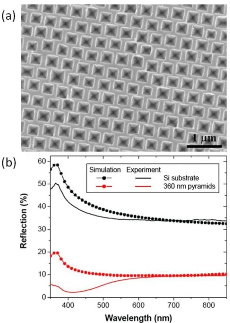
As shown in Fig. 1-7, C. H. Sun et al. fabricated periodic inverted pyramid array by colloidal lithography and KOH wet etching [15]. The reflectance in visible range was about 6%. The simulated result by using RCWA was compared to the measured reflection spectrum. The two spectra had a good agreement with each other in long wavelength but they had some deviation in short wavelength.
The best three structures, pillar with round top, pillar with cone top and cone array, are mentioned. RCWA or TFT simulation can be used to provide some information to determine how low the reflectivity of the structure can be. Some papers show that fill factor has important influence on reflectivity [11]. In other words, the base area of the anti-reflective structure should be as large as possible.
Fig. 1-7 (a) Inverted pyramid structure on a silicon substrate (b)Experimental (solid) and RCWA-simulated (dotted) specular optical reflectivity at normal incidence. Black:
bare (100) silicon wafer. Red: 360 nm size pyramids template from 320 nm silica spheres [15].
1-1-3 Hydrophobic and Anti-Reflective Nano
Structure
From discussion above, nano structure with small top area and proper shape can have high contact angle and low reflectivity. Recently, some papers reported on the fabrication of micro or nano structures which have the two properties simultaneously.
As shown in Fig. 1-8, Y. C. Chang et al. fabricated inverted pyramid array on silicon substrate by electron beam lithography and KOH wet etching in 2007 [16].
The period of the structure was 300 nm and the height was 212 nm. The aspect ratio of the structure was 0.7. The nano structure was coated with Teflon film and the wettability of the surface was changed from hydrophilic to hydrophobic. The average reflectance of the nano structure in visible range was 17%. The contact angle of the structure was 135.9o. The theoretical contact angle of the nano structure was 142.7 o and the case was in Wenzel state. The two contact angles are very close. The sliding angle was not reported.
As shown in Fig. 1-9, W. L. Min et al. fabricated periodic pillars array on silicon substrates by colloidal nano particles and reactive ion etching in 2008 [17].
The period of the structure was 98 nm and the height was 400 nm. The aspect ratio of the structure was 4.08.
Fig. 1-8 Inverted pyramid arrays on a silicon substrate [16].
Fig. 1-9 Silicon nanopillar array fabricated by nano particles and reactive ion etching [17].
The average reflectance of this nano structure in visible range was 1.58%. The structure was then fluorosilane modified. The measured contact angle of the modified nano structure was 158 o. The sliding angle was not reported here.
In 2009, Y. F. Li et al. fabricated biomimetic silicon hollow-tip arrays by using metal catalytic wet etching silicon followed by a short time reactive ion etching process [18]. The initial pattern was achieved by non close packed polystyrene particles. The tip arrays were vertical to the substrate with 686 nm in root diameter, 792 nm spacing, and 7.1μm in height. The SEM graph of the tip arrays are shown in Fig. 1-10. The aspect ratio of the needle array was higher than 12. From Fig. 1-11, the TEM image of the silicon tip, we can see straight pores inside, and the distribution of pores in the tip was random. The diameters of the pores were about 50–150 nm. The specular reflectance in the 250-1600 nm was lower than 1%. The measured water contact angle was 165o for the 7.1μm height hollow-tip arrays which was fluorosilane modified. The sliding angle was 2°. Actually, the artificial mirco or nano structures which possess both low reflectivity and hydrophobic property usually have high aspect ratios. The aspect ratios of these structures are usually higher than 4.
Many structures with moth-eye effect observed from butterfly usually have low aspect ratio. The aspect ratio of the structures on the surface of butterfly is usually lower than 2 [9].
Fig. 1-10 High aspect ratio hollow-tip array on silicon substrate [18].
Fig. 1-11 TEM image of the hollow-tip detached from the substrate [18].
This phenomenon may be explained by the requirement of mechanical strength.
Intuitively, micro or nano structure with low aspect ratio can bear higher mechanical loading. In the field of micro or nano engineering, nano structures with high aspect ratio have bad durability and make nano imprint process much harder.
The complex nano structure on cicada wing introduced by G.Y. Xie et al. [3] fit the two geometric requirements: small top area and large base area. The structure had low aspect ratio which was 2. The definition of aspect ratios for a dual structure is shown in Fig. 1-12. The authors replicate the nano structure from cicada wing to PMMA by gold evaporation and nano imprint. The replica of PMMA shows one fourth reflectance than that of a flat PMMA film. Other report also showed that cicada wing had anti wetting property [19]. The contact angle of cicada wing could be as high as 147o.
In this thesis, we introduce a process to fabricate subwavelength dual structure which was inspired by the structure of cicada wing. We also demonstrate that the dual structure can possess both anti-reflection and low sliding angle simultaneously.
Fig. 1-12 A general shape of dual structure. The aspect ratio of top part is defined by h1/w1. The aspect ratio of the total structure is defined by h2/w2.
1-2 Organization of the Thesis
In Chapter 2, grating equation, TFT and effective medium theory (EMT) will be introduced briefly. The three theories provided intuitive physical meaning of anti-reflective structures. RCWA, a much more accurate model for reflectance simulation of anti-reflective subwavelength structures will also be introduced. The simulated reflectance of complex subwavelength structure array will be compared to the simulated reflectance of bell-shaped structure and cone structure.
In Chapter 3, the whole fabrication process of complex structure will be presented. The modulation of structure shape by changing exposure dosage, RIE parameter, and ICP-RIE parameter will also be described.
In Chapter 4, the measured reflectance, contact angle, and sliding angle of our dual structure will be shown.
In Chapter 5, the conclusion of current work and results will be made. Possible future works will also be described.
Chapter 2. Design and Simulation
In this chapter, modeling of subwavelength optics will be shown. Some rules and theories for designing hydrophobic and anti-reflective structures will be discussed.
Main focus will be on the design of anti reflection structure, because the rule for designing hydrophobic structure is simple: sharp peaks.
2-1 Grating Equation, TFT and EMT
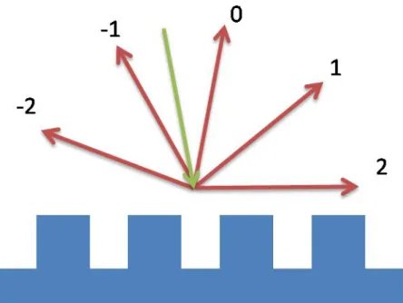
In our laboratory two-beam interference lithography was made to generate periodic patterns. By Eq. (2.1), the grating equation, the period of nano structure should be smaller than the wavelength of normal incident light to prevent reflective light of higher orders. The phenomenon is shown in Fig. 2-1 and Fig. 2-2.
m a
sin
sin
(2.1)where is the incident angle of the light,
is the reflected angle of the light, and a is the period of the structure.Fig. 2-1 Reflective light of higher order appears when the period of the grating is larger than the wavelength.
Fig. 2-2 Only reflective light of zero order appears when the period of the grating is smaller than the wavelength of incident light and the angle of incident light is not large.
Anti-reflective coating is a common topic in TFT. A general way to eliminate reflection between two different mediums is to insert one or more layers between the two medias. The refractive indices of these inserted layers should be between the refractive indices of the two mediums and this can creates a continuous refractive index gradient. The combination of TFT and EMT provided an intuitive physical meaning of anti-reflective structure. As shown in Fig. 2-3, a periodic subwavelength structure can be optically equivalent to thin film layers. The effective refractive index of each layer is decided by the volume ratio of every substance involved in that layer.
The simplest way to represent the refractive index of each layer is by linear combination of refractive indices (Eq. (2.2)).
2
f) 1
-
(1
f , (2.2) where f is the volume fraction of the first substance in each layer, 1 is the refractive index of the first substance, 2is the refractive index of the second substance.
When the structure is positively tapered, the structure can be optically equivalent to many thin film layers that creates a continuous refractive index gradient and the anti reflection is thus achieved. Positively tapered structure means that the diameter of the structure increases from top to bottom. In order to match the refractive index to the substrate, the fill factor of the structure should be as large as possible. The fill factor means the ratio of the base area to the area of a unit cell.
Fig. 2-3 Subwavelength structure is divided into nine layers.
2-2 Simulated Reflectance of Bell-shaped Structure, Cone
structure, and Dual Structure by Using RCWA
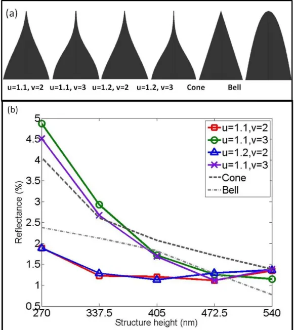
From the discussion of Section 2-1 and Chapter 1, a subwavelength structure should have sharp peak and high fill factor to achieve anti reflection and hydrophobicity simultaneously. Furthermore, the aspect ratio of the structure is also considered for durability. Our goal of the aspect ratio is under 2. Since the period of our two-beam interference is set to 270 nm, the goal of the structure height is set to be under 540 nm. To achieve the goal, an error function is used to model the subwavelength structure.
(z) = erf(z × v − h × u × v) + c (2.3) where z is the distance from the top of the structure, u is used to change the z position of inflection point, v is used to change the slope at the inflection point, c was used to change the top area of the structure (usually equals to 1), and h is the total structure height . The structure described by this function is shown in Fig. 2-4.
RCWA, an accurate tool for optical simulation, was used to simulate the reflectance of the structures. The computation step was set to be 40 nm. The period of a unit square lattice was 270 nm. The simulated wavelength was in the visible range which was from 400 nm to 700 nm.
Fig. 2-4 General structure for simulation.
In order to find an optimized solution efficiently, average reflectance was the major value to be lowered. The average reflectance of the structure described by error function of different u and v will be compared.
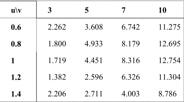
Firstly, h was set to be 540 nm and then different u and v were applied to observe the variation of average reflectance. u was set to be 0.6, 0.8, 1, 1.2 and 1.4. v was set to be 3, 5, 7, and 10. The results are shown in Table 2-1. The lowest average reflectance in this table occurs when u is 1.2 and v is 3. To find a better solution, u was set to be 1.1, 1.2, 1.3 and v was set to be 2, 3, and 4. The results are shown in Table 2-2. It can be seen that average reflectance can be further lowered when u is 1.1 and v is 3.
Now variable h was also changed to observe the variation of average reflectance.
h are set to 270, 337.5, 405, 472.5, and 540 nm. u was set to be 1.1 and 1.2. v was set to be 2 and 3. The results are shown in Fig. 2-5. Here the average reflectance of cones array and bell-shaped structures array are also plotted in Fig. 2-5. It can be seen the dual structures have lower reflection at lower structure height (<475 nm) at u of 1.1 and v of 2.
When u was changed from 1.1 to 1.2, the inflection point shifted 5% of total structure height at z direction. When v was changed from 2 to 3, the slope at inflection point became 1.35 times larger.
u\v 3 5 7 10 0.6
2.262 3.608 6.742 11.2750.8
1.800 4.933 8.179 12.6951
1.719 4.451 8.316 12.7541.2
1.382 2.596 6.326 11.3041.4
2.206 2.711 4.003 8.786Table 2-1 Average reflectance corresponding to different u and v at height 540 nm.
u\v 2 3 4
1.1
1.347 1.148 1.871.2
1.366 1.382 1.4331.3
1.756 1.516 1.483Table 2-2 Average reflectance corresponding to different u and v at height 540 nm.
Fig. 2-5 (a) Structure shapes for simulation (b) Average reflectance of dual structures, cones array, and bell-shaped structures array corresponding to different structure heights.
2-3 Summary
In this chapter, the average reflectance of dual structure, cones array, and bell-shape structures are compared by changing the heights of these structures. The simulation results show that the reflectances of dual structure with v of 2 and u of 1.1 or 1.2 are lower than those of cones array and bell-shaped structures when the heights of the structures are smaller than 470 nm. The results show that dual structures with v of 2 and u of 1.1 or 1.2 can be an efficient structure since it can provide low reflectance with low aspect ratio. Besides, this shape also has sharper peak than cone shape, and thus it can provide better hydrophobicity and lower sliding angle.
Chapter 3. Fabrication
The dual structure on a cicada wing has been revealed by G.Y. Xie et al. [3].
Though the structure could be replicated on PMMA films by Au deposition and nano-imprint, the size of the structure could not be made change. Furthermore, the size of the sample was limited by the original cicada wing. In this chapter, we will show how to fabricate dual structure on a silicon substrate. The whole processing steps are shown in Fig. 3-1.
Fig. 3-1 Processing steps.
3-1 ARC and PR Coating
First, we get thermal oxidized wafers from NDL (National Nano Device Laboratories). 60nm thick silicon dioxide is grown on each wafer. Prior to spin coating, RCA clean process should be applied. Next, anti-reflection coating (ARC) and photoresist (PR) are coated layer by layer by using a spin coater. The specific parameters of ARC and photoresist coating are shown in Table 3-1. ARC, HXRIC-16, is provided by Brewer Science Asia. Photoresist, Sumiresist PFI-34A2, is provided by Sumitomo Chemical.
The thickness of ARC layer should be controlled very accurately. The reflectance in the interface of ARC and PR changes with the variation of ARC thickness. In subsequent lithography process, the reflectance in the interface of ARC and PR has bad influence on profile of PR patterns.
If the reflectance in the interface of ARC and PR approaches zero, the sidewall of the PR pattern will be vertical and there will be no residue PR layer between the PR patterns and ARC. On the contrary, if the reflectance in the interface of ARC and PR is higher than 1%, there will be residue PR layer and there will be standing wave on side wall of the PR pattern. The residue PR layer made subsequent etching process unstable because it should take one more etching process to remove the residue PR layer before performing subsequent process. The residue PR layer not only needs one
more process step to remove it but also makes the height of the PR pattern lower since the original thickness of the PR layer is held constant by the coating process.
To achieve the lowest reflectance in the interface of ARC and PR, the most suitable thickness of ARC is calculated by thin film theory. As shown in Fig. 3-2, the lowest reflectance in the interface of ARC and PR can be achieved when the thickness of ARC is 128nm. Referring to the data sheet of ARC shown in Fig. 3-3 [23], it was found that the 128 nm thickness of ARC could be achieved by setting rotation speed of spin coater to 3200 rpm. In fact, the rotation speed of spin coater is set to be 5500 rpm. Due to storage condition and continual degradation of ARC, the parameters for ARC coating change day by day.
After ARC layer is coated on the wafer, the wafer is baked on a hot plate with temperature at 175 o C for 60 seconds. This process drives the solvent away and releases some residue stress in the structure of ARC film.
It is desired to have thicker PR layer in considering the process of pattern transfer to ARC and silicon dioxide. Pattern transfer to ARC and silicon dioxide is not the only factor in determining the thickness of the PR layer. The thickness of PR layer should be controlled to prevent the PR pattern from collapsing.
Fig. 3-2 Reflectance in the interface between PR and ARC layers.
Fig. 3-3 Spin speed curve of ARC [20].
The PR pattern is prone to collapse if the aspect ratio of the PR pattern was higher than 2. The thickness of PR layer should be larger than the thickness of ARC.
The thickness of the PR layer was determined to be 200 nm. Referring to the data sheet of the PR shown in Fig. 3-4 [24], it is found that 200 nm thickness of PR layer could be achieved by setting the rotation speed of spin coater to 4000 rpm. In our experiment, the rotation speed of PR coating is set to 4000rpm and the thickness of PR is 224 nm.
After PR is coated on wafer, the wafer is soft-baked on a hot plate at temperature of 110oC for 60 seconds. The baking process drives the solvent in PR away and makes the film property stable. The specific baking parameters are listed in Table 3-2. After the wafer is baked, the wafer is cut into 7 smaller chips for subsequent processing.
Fig. 3-4 Spin speed curve of PR [21].
Table 3-1:Coating parameters of ARC and photoresist.
1st step 2nd step
speed (rpm) time (seconds) speed (rpm) time (seconds)
ARC 500 18 5500 60
PR 500 10 4000 60
Table 3-2:Baking parameters of ARC and PR.
soft bake post bake hard bake
temperature time temperature time temperature time
(℃) (seconds) (℃) (seconds) (℃) (seconds)
ARC 175 60
PR 90 60 110 60 140 60
3-2 Two-beam Interference Lithography
3-2-1 Exposure Principle of Two-beam Interference
Lithography
Two-beam interference lithography is a simple method in fabricating large area periodical nano patterns. In comparison with E-beam lithography, two-beam interference lithography could be more economic and time-saving. As shown in Fig.
3-5, this is our whole exposure system.
The period of grating pattern which is fabricated by two-beam interference lithography can be expressed by
sin
2
(3.1) where is the period, is the wavelength of incidence, and is the angle of incident light.
3-2-2 Exposure and Development
The chip coated with ARC and PR was placed on a stage and then the exposure was performed. As mentioned above, the PR recorded the dosage distribution of the two-beam interference image which was spatially sinusoidal.
Fig. 3-5 Exposure system of two-beam interference lithography.
After development of the exposed chip, PR grating pattern was formed on the chip. To achieve two dimensional PR patterns, the chip was exposed with half exposure dosage and the chip was rotated ninety degrees to perform another exposure with half exposure dosage.
The PR in our experiment was positive type. There was a threshold of exposure dosage for the positive PR to be washed out in the development. The PR with exposure dosage higher than the threshold will be washed away in development.
The PR pattern can be made to be posts array or holes array by changing the total exposure dosage. For example, we assume the dosage distribution of the interference pattern as shown in Fig. 3-6 and Fig. 3-7, and the exposure threshold of the PR is 40 (arbitrary unit, the same with the unit of the color bar in Fig. 3-6 and Fig. 3-7). The dosage distribution shown in Fig 3-6 will result in PR pattern to be posts array after development because only the deep blue part of the PR in Fig. 3-6 remains. The dosage distribution shown in Fig. 3-7 will result in holes array of PR pattern after development because the red part of the PR in Fig. 3-7 will be washed away. As shown in Fig. 3-8 and Fig. 3-9, the PR pattern of posts array can be made by exposing higher total dosage and the PR pattern of holes array can be made by exposing lower total dosage.
Fig. 3-6 Two-beam interference image with higher exposure dosage.
Fig. 3-7 Two-beam interference image with lower exposure dosage.
Fig. 3-8 SEM image: PR pattern of posts array (total exposure dosage: 58mJ).
Fig. 3-9 SEM image: PR pattern of holes array (total exposure dosage: 42mJ).
In our experiment, higher total exposure dosage was chosen to make the final PR pattern to be posts array. Various total exposure dosage can be achieved by changing the exposure time. As shown in Fig. 3-5, the shutter which was driven by computer can control the exposure time very precisely. After exposed by using the two-beam interference lithography system, the chip was baked on the hot plate at temperature of 110oC for 60 seconds. After post baked, the chip was developed by EPD-1000 for 60 seconds. EPD-1000 was the standard developer of our PR which was provided by Everlight Chemical Industrial Co. The development was composed of 2.38%
Tetramethylammonium hydroxide. The top view and side view of the posts array PR pattern are shown in the SEM images, Fig. 3-8 and Fig. 3-10. The period of our PR pattern was 270nm.
Fig. 3-10 SEM image: side view of PR pattern of posts array.
3-3 Pattern Transfer to ARC and Silicon Dioxide by
RIE
After the PR pattern of posts array has been achieved, we started to transfer the pattern from PR layer to ARC and silicon dioxide. Silicon dioxide was used to be the mask of subsequent ICP process. The ICP process will be discussed in the following section.
In considering the geometry and scale of our pattern, anisotropic etch was needed. RIE (Samco RIE 10NR) in this step was used.
The first step of dry etching process in our experiment is to transfer pattern from PR to underlying ARC layer. ARC, a species of polymer, is usually etched by oxygen-based RIE in dry etching process. Here, CF4 (25sccm) and O2 (6sccm) were used as the feeding gases of RIE to transfer pattern from PR to ARC layer. In our experiment, the power of RIE was set to 150W and the pressure is set to 1.3 Pa.
The mechanism of CF4/O2 RIE to etch polymer was discussed by A. M. Wrobel et al. [22]. The oxygen atoms caused aromatic ring opening and increased carbonyl (C
= O) bond concentration. They found addition of CF4 to O2 dramatically increased the etch rate. First, even small amounts of CF4 (<10%) could result in oxygen atomic concentration. Secondly, atomic fluorine was produced by dissociation of the CF4
molecule. Fluorine atoms could abstract hydrogen atoms from the polymer, thus creating radical sites on the surface which readily undergo reactions with oxygen atoms.
The hydrogen abstraction by fluorine ions is sufficiently exothermic to cleave carbon-carbon bonds. Combined with carbon-oxygen bonds formation with oxygen atoms, this eventually leads to the observed volatile reaction products. When the ration of CF4 in the mix CF4/O2 gases increases to a certain level, the polymer surface is passivated by the formation of chemically stable fluorocarbon groups which strongly impede the etching process.
This phenomenon may lead to some good property in our experiment because of the vertical side wall of the PR pattern can be protected by the fluorocarbon layer.
Addition of CF4 to the etching gases lead to inhibitor layer on the whole surface of the PR pattern. Since the ions bombarded the samples mostly in the vertical way, the side wall which is protected by the fluorocarbon layer is not etched. On the contrary, the etching gas chemistry of pure oxygen leads to certain critical dimension loss without inhibitor layer on the side wall of the PR pattern.
The second step of our dry etching process is to transfer ARC pattern to silicon dioxide layer. In this step CHF3 (30 sccm) was chosen as the feed gas chemistry in RIE. Referring to some text book about semi-conductor technology, we used CHF3 to
etch silicon dioxide. In this step the pressure was set to 1.3 Pa and the power of RIE was set to 100W. The etching time was 260 seconds. Then the ARC pattern was etched by RIE with O2 gas. This process reduced the ARC posts to smaller sharp tips.
The final ARC and silicon dioxide patterns are shown in Fig. 3-11.
Fig. 3-11 AFM image of ARC and silicon dioxide pattern.
3-4 Pattern Transfer from ARC and Silicon Dioxide
Pattern to Silicon Substrate by ICP-RIE
In this step ARC and silicon dioxide pattern was transferred to silicon substrate to form dual structure by ICP. The etching tool we used in this step was Elionix EIS-700 Inductively Coupled Plasma Etching system. The ICP system was shown in Fig. 3-14. This ICP system is located in the Institute of Physics, Academia Sinica. The ICP recipe is shown in Table 3-4. Initially negative tapered structure was fabricated by recipe 1 which was provided by the manager of this ICP system. Negative tapered pillar structure means the diameter of the topper part is larger than the diameter of the base. To make the slope of the pillar from negative to positive, process time for passivation was increased. When the process time in recipe 3 was increased to 9 seconds, the structure became positive tapered. The influence of passivation time on profile control is shown in Fig. 3-13. The results fabricated by ICP recipes 1, 2, and 3 in Table 3-4 are shown in Fig. 3-13 (a), (b), and (c). Addition of oxygen in etching gas also helps to fabricate positive tapered structure. The addition of oxygen can lower SF6 ratio in the etching gas flow and the etching rate is suppressed. The influence of oxygen flow rate on profile control is shown in Fig. 3-14. The results fabricated by ICP recipes 1, 2, and 3 in Table 3-4 are shown in Fig. 3-14 (a), (b) and
(c).The dual structures were fabricated by recipe 2, 6, and 9. These dual structures are shown in Fig. 3-15, Fig. 3-16, and Fig. 3-17 Dual structure C respectively. The upper part of the structure was shorter than the lower part because silicon dioxide was a stronger mask than ARC. The side wall of the structure shown in Fig. 3-15 is more vertical than the side wall of the structure shown in Fig. 3-16 because the structure is prone to be vertical by using recipe 2.
Fig. 3-12 ICP system located in the Institute of Physics, Academia Sinica.
Fig. 3-13 The influence of passivation time on profile control. Passivation time:(a) 6s (b) 7.5s (c) 9s.
Fig. 3-14 The influence of oxygen flow rate on profile control. Oxygen flow rate:(a) 0sccm (b) 2sccm (c) 7sccm.
Fig. 3-15 Dual structure A.
Fig. 3-16 Dual structure B.
Fig. 3-17 Dual structure C.
3-5 Tunable Ratio of the Heights between Upper Part
and Lower Part of the Structure
In Section 3-4, the dual structure with shorter upper part is fabricated. In this section, the process for fabricating dual structure with shorter height of the lower part will be described.
As shown in Fig. 3-1, one more RIE process was performed after O2 etching process. In this step, the etching gas was CHF3 and the recipe was the same as the recipe used to transfer pattern from ARC to silicon dioxide. The etching time of this step was 45 seconds. After this RIE step, ICP process was performed to transfer pattern into silicon substrate. The fabrication results are shown in Fig. 3-18 and Fig.
3-19. By performing one more CHF3 RIE step, the dual structures with shorter lower part were fabricated because part of the uncovered Si dioxide mask was etched.
Fig. 3-18 Dual structure D.
Fig. 3-19 Dual structure E.
Table 3.4 ICP-RIE parameters.
Platen (W)
Bias (V)
Etch time (s)
SF6
(sccm) O2
(sccm)
Platen (W)
Bias (V)
process time(s)
C4F8
(sccm) 1
600 200 2 20 0 400 0 6 50
2
600 200 2 20 0 400 0 7.5 50
3
600 200 2 20 0 400 0 9 50
4
600 200 2 20 2 400 0 7.5 50
5
600 200 2 20 7 400 0 7.5 50
6
600 200 2 20 2 400 0 9 50
7
600 200 2 20 0 400 0 8.3 50
8
600 200 2 20 0 400 0 7.6 50
9
600 150 2 20 12 400 0 9 50
10
600 150 2 20 0 400 0 7.5 50
11
600 0 0 0 0 400 0 10 50
3-6 Surface Modification
The dual structures were surface modified by ICP-RIE. The surface modification process was performed by using the 11th recipe of ICP-RIE which is listed in Table 3.4. The deposited fluorocarbon film was hydrophobic and had a static water contact angle of 109°.
3-7 Summary
In this chapter, the fabrication process of dual structures is detailed. The overall diameter of the structures can be modified by initial exposure dosage of two-beam interference. The sharp tips of the dual structures can be formed by using O2 RIE to reduce the ARC posts pattern to small sharp tips pattern. The height of the lower part of dual structure can be reduced by one more CHF3 RIE process after O2 RIE process.
Chapter 4. Measurement
In this chapter, the measurement results of contact angles and sliding angles of our dual structures will be reported. Measured reflection spectra of our dual structures will also be shown.
4-1 Measurement of Contact Angle and Sliding Angle
As mentioned in Chapter 1, an intuitive way to describe the wettability of a solid surface is by measuring its contact angle. For self-cleaning property, sliding angle is more important than contact angle. Here the two angles will be measured. The setup of the contact angle analyzer is shown in Fig. 4-1 Contact angle analyzer, which is home made. The home made setup for sliding angle measurement is shown in Fig. 4-2 and Fig. 4-3. The setup for sliding angle measurement was consisted of a laser pointer and a concentric ruler. As shown in Fig. 4-3 (a), the laser pointer was calibrated by a wafer floating on water. The laser light shot to the wafer floating on water and then shot back to the laser pointer. This process made sure that the laser light was parallel to a plumb line. As schematically shown in Fig. 4-3 (b), the sample was placed at a stage that can tilt small angles. A 20 μl water drop was placed on the sample and the stage started to tilt, once the water drop slide and the distance from the laser pointer and the reflected laser light on the concentric ruler was recorded. The sliding angle
can be calculated by Eq. (4.1).
= (arctan(d/L))/2 (4.1) The setup of sliding angle measurement shown in Fig. 4-3 is used to measure low sliding angle (<5o). When the sliding angle is larger than 5o, another setup of sliding angle measurement is used, which is shown in Fig. 4-4 Setup for sliding angle measurement.
The measured contact angles and sliding angles of dual structures are listed in Table 4.1. The shapes of the 5 dual structures are also shown. From Table 4.1, the 5 types of dual structures are all superhydrophobic. The sliding angles of these dual structures were all lower than 5°. The sharp peaks of the dual structures are smaller than 75 nm in diameter. In comparison to the dual structures which have sharp peaks, the simple structures with larger top diameters have larger sliding angles. The measured contact angles and sliding angles of 3 simple structures are listed in Table 4.2. The structure shapes are shown in Fig. 4-6.The sliding angles of the 3 simple structures are all larger than 18o. The top diameters of the simple structures are larger than 140 nm. The top diameter of the three structures which are shown in Fig. 4-6 (a), (b), and (c) are 150, 160, and 220 nm, respectively. From the results, the sharp peaks of the subwavelength structures did help to have low sliding angles.
Fig. 4-1 Contact angle analyzer.
Fig. 4-2 Setup for sliding angle measurement for <5o.
Fig. 4-3 Setup for sliding angle measurement (a) First calibration (b) Then sliding angle measurement.
Fig. 4-4 Setup for sliding angle measurement >5o
Table 4.1 The contact angles and sliding angles of dual structures. The corresponding structure shapes are shown in the figures below.
Contact angle Sliding angle
A 157° 4.5°
B 155° 2.4°
C 162° 2.7
D 157° 3°
E 162° 1.8°
Fig. 4-5 Dual structure A, B, C, D, and E.
Table 4.2 The contact angles and sliding angles of simple structures. The corresponding structure shapes are shown in the figures below.
Contact angle Sliding angle
I 150o 18o
II 146o 20o
III 137o 37o
Fig. 4-6 Simple structures.
4-2 Measurement of Reflectance
The reflectance spectra of the dual structures were measured by our home made reflectometer shown in Fig. 4-7.
The measured reflectance spectra of our 5 dual structures are shown in Fig. 4-8.
The structure shapes of the 5 dual structures are shown in Fig. 4-5.
The dual structure A has the highest reflectance because it has negatively tapered side wall. The dual structure D and E have higher reflectance than that of dual structure B and C. The increased reflectance of dual structure D was due to its low fill factor. The increased reflectance of dual structure E was due to its vertical side wall.
The dual structure B has lower reflectance than that of dual structure A, D, and E and its average reflectance is 3.83%. The optical response of dual structure B is similar to the optical response of the structure shapes shown in Fig. 4-9 (b). The three shapes shown in Fig. 4-9 (b) are described by Eq. (2.3) and v is 4 here. From the v value, it can be understood that the increased reflectance of dual structure B over 500 to 700 nm is caused by the obvious transition between top part and bottom part.
The dual structure C has the lowest average reflectance. The reflectance of dual structure is lower than 5% at 400 to 700 nm and its average reflectance is 1.8%. The slope of the side wall slightly changes in the middle of the structure. The reflectance spectrum of dual structure C and the reflectance spectra of the better 2 structure
shapes proposed in Chapter 2 are shown in Fig. 4-10 (c). The reflectance spectra of the 3 structures are all lower than 5% from 400 to 700 nm but the spectra are different.
This may be due to the peak of the shapes proposed in Chapter 2 is sharper than the peak of dual structure C. Moreover, the uniformity of dual structure C is not so perfect and causes the structure shape deviation between each pillar. The deviation may also cause the reflectance spectrum to be changed. The sample picture of dual structure C is shown in Fig. 4-11. The dark red color indicates that there is scattering lights from the sample.
Fig. 4-7 Setup for reflectance measurement.
Fig. 4-8 Measured reflectance spectra of 5 dual structures and flat silicon.
Fig. 4-9 (a) Dual structure B (b) Reflectance spectra of dual structure B and simulated SWSs. The shapes shown in the up-left corner were used for simulation and the structure height for simulation is 540 nm. The 3 shapes were described by Eq. (2.3) and v was 4 here.
Fig. 4-10 (a) Structure shapes for simulation and the structure height is set to 405 nm (b) Dual structure C (c) Simulated reflectance spectra of Fig. 4-10 (a) and flat silicon and measured reflectance of dual structure C.
Fig. 4-11 Sample picture of dual structure C.
Chapter 5. Conclusion and Future Work
5-1 Conclusion
Subwavelength dual structures were fabricated. Dual structure C had 1.8%
average reflectance and 2.7o sliding angle. Though the shape of dual structure C did not match the shape we proposed in Chapter 2 perfectly but it did possess both anti-reflection and low sliding angle simultaneously. The top part aspect ratio of dual structure C is 2 and the total aspect ratio of dual structure C is 1.5. The aspect ratios of dual structure C show that it has good mechanical durability.
The ARC pattern reduction process introduced in Section 3-3 made the Si dual structure had sharp tips, and the tips were confirmed to help the structures have low sliding angles.
The methods for shape modulation are discussed in Section 3-7, and these parameters used in the methods can be further modified to approach better shape and thus the dual structures can have better anti-reflection or sliding angle.
5-2 Future Work
Though dual structure C possesses both good anti reflection and low sliding angle simultaneously, there is still something to be improved about this structure.
Reproducibility is the first issue. More samples should be made by the same process and parameters. The large amounts of samples are used to confirm the reproducibility.
Uniformity is the second issue. From AFM image shown in Fig. 3-11, we can find out that the uniformity of the small ARC dots on silicon dioxide post is not very good. The ARC dot is not always located at center of the silicon dioxide post. The RIE parameters of oxygen plasma should be modified to improve the uniformity.
Decreasing flow rate of oxygen in RIE process is a possible solution.
Manufacturing is the third issue. Nano-imprint process is a good way to mass production or replication. The structure height of dual structure C is only 406 nm and the aspect ratio of it is only 1.5. The low structure height and aspect ratio make it possible for dual structure C to be manufactured by using nano-imprint.
References
1. W. Barthlott and C. Neinhuis, "Purity of the sacred lotus, or escape from
contamination in biological surfaces," Planta, Vol. 202, pp. 1-8 (1997).
2. X. F. Gao and L. Jiang, "Biophysics: Water-repellent legs of water striders,"
Nature, Vol. 432, pp. 36-36 (2004).
3. G. Y. Xie, G. M. Zhang, F. Lin et al., "The fabrication of subwavelength
anti-reflective nanostructures using a bio-template," Nanotechnology, Vol. 19, 095605 (2008).
4. R. N. Wenzel, "Resistance of solid surfaces to wetting by water," Ind. Eng.
Chem. Res., Vol. 28, pp. 988-994 (1936).
5. A. B. D. Cassie and S. Baxter, "Wettability of porous surfaces," Trans. Farad.
Soc., Vol. 40, pp. 0546-0550 (1944).
6. E. Hosono, S. Fujihara, I. Honma et al., "Superhydrophobic perpendicular
nanopin film by the bottom-up process," J. Am. Chem. Soc., Vol. 127, pp.
13458-13459 (2005).
7. M. H. Jin, X. J. Feng, L. Feng et al., "Superhydrophobic aligned polystyrene
nanotube films with high adhesive force," Adv. Mater., Vol. 17, pp. 1977 (2005).
8. C. J. Lv, C. W. Yang, P. F. Hao et al., "Sliding of Water Droplets on
Microstructured Hydrophobic Surfaces," Langmuir, Vol. 26, pp. 8704-8708 (2010).
9. D. G. Stavenga, S. Foletti, G. Palasantzas et al., "Light on the moth-eye corneal
nipple array of butterflies," Proc. Soc. Exp. Biol. Med., Vol. 273, pp. 661-667 (2006).
10. Chih-Hung Sun, Peng Jiang, and Bin Jiang, "Broadband moth-eye antireflection
coatings on silicon," Appl. Phys. Lett., Vol. 92, 061112 (2008).
11. H. M. Wu, C. M. Lai, and L. H. Peng, "Optical response from lenslike
semiconductor nipple arrays," Appl. Phys. Lett., Vol. 93, 211903 (2008).
12. S. Wang, X. Z. Yu, and H. T. Fan, "Simple lithographic approach for
subwavelength structure antireflection," Appl. Phys. Lett., Vol. 91, 061105 (2007).
13. Y. Kanamori, M. Sasaki, and K. Hane, "Broadband antireflection gratings
fabricated upon silicon substrates," Opt. Lett., Vol. 24, pp. 1422-1424 (1999).
14. H. L. Chen, S. Y. Chuang, C. H. Lin et al., "Using colloidal lithography to
fabricate and optimize sub-wavelength pyramidal and honeycomb structures in solar cells," Opt. Express, Vol. 15, pp. 14793-14803 (2007).
15. C. H. Sun, W. L. Min, N. C. Linn et al., "Templated fabrication of large area
subwavelength antireflection gratings on silicon," Appl. Phys. Lett., Vol. 91, 231105 (2007).
16. Y. C. Chang, G. H. Mei, T. W. Chang et al., "Design and fabrication of a
nanostructured surface combining antireflective and nhanced-hydrophobic effects," Nanotechnology, Vol. 18, 285303 (2007).
17. W. L. Min, P. Jiang, and B. Jiang, "Large-scale assembly of colloidal
nanoparticles and fabrication of periodic subwavelength structures,"
Nanotechnology, Vol. 19, 475604 (2008).
18. Y. F. Li, J. H. Zhang, S. J. Zhu et al., "Bioinspired silicon hollow-tip arrays for
high performance broadband anti-reflective and water-repellent coatings," J.
Mater. Chem., Vol. 19, pp. 1806-1810 (2009).
19. T. L. Sun, L. Feng, X. F. Gao et al., "Bioinspired surfaces with special
wettability," Acc. Chem. Res., Vol. 38, pp. 644-652 (2005).
20. Spin speed curve of HXRIC-16, Brewer Science Asia (2006).
21. Spin speed curve of Sumiresist PFI-34A2, Sumitomo Chemical.
22. A. M. Wrobel, B. Lamontagne, and M. R. Wertheimer, "Large-Area
Microwave and Radiofrequency Plasma-Etching of Polymers," Plasma. Chem.
Plasma. P., Vol. 8, pp. 315-329 (1988).
![Fig. 1-1 An SEM image of a lotus leaf shows the two-scale roughness [1].](https://thumb-ap.123doks.com/thumbv2/9libinfo/9607330.633083/12.892.139.754.444.824/fig-sem-image-lotus-leaf-shows-scale-roughness.webp)
![Fig. 1-3 An SEM image of a cicada wing [3].](https://thumb-ap.123doks.com/thumbv2/9libinfo/9607330.633083/14.892.265.631.331.800/fig-sem-image-cicada-wing.webp)
![Fig. 1-6 Measured reflectance spectrum and simulated reflectance spectra by using RCWA and TFT models [11]](https://thumb-ap.123doks.com/thumbv2/9libinfo/9607330.633083/22.892.145.754.331.802/measured-reflectance-spectrum-simulated-reflectance-spectra-using-models.webp)
![Fig. 1-9 Silicon nanopillar array fabricated by nano particles and reactive ion etching [17]](https://thumb-ap.123doks.com/thumbv2/9libinfo/9607330.633083/27.892.141.762.307.857/fig-silicon-nanopillar-array-fabricated-particles-reactive-etching.webp)
![Fig. 1-10 High aspect ratio hollow-tip array on silicon substrate [18].](https://thumb-ap.123doks.com/thumbv2/9libinfo/9607330.633083/29.892.175.787.146.799/fig-high-aspect-ratio-hollow-array-silicon-substrate.webp)