ZnO hexagonal microboxes enclosed only by
ˆ0001‰ facets with epitaxial
nanowalls
Ruey-Chi Wang
Department of Chemical and Materials Engineering, National University of Kaohsiung, Kaohsiung 811, Taiwan
Chuan-Pu Liua兲and Jow-Lay Huang
Department of Materials Science and Engineering, National Cheng Kung University, Tainan 70101, Taiwan and Center for Micro/Nano Science and Technology, National Cheng Kung University, Tainan 70101, Taiwan
共Received 29 April 2006; accepted 10 September 2006; published online 25 October 2006兲 Hexagonal ZnO microboxes constructed of ZnO 兵0001其 facets with vertical and horizontal single-crystalline nanowalls were synthesized on Si共001兲 via a self-assembled process by thermal chemical vapor deposition. High-resolution transmission electron microscopy images show that ZnO sheets with nanowalls on top can be assembled at 86° and 62° to each other by twinning and epitaxy, respectively. The room-temperature cathodoluminescence spectrum of the microboxes shows a strong and sharp ultraviolet emission as well as a negligible green emission. The vertical and horizontal nanowalls have potential to be applied as templates for growth of vertically and horizontally aligned nanowires for three-dimensional nanoelectronics. © 2006 American Institute of Physics. 关DOI:10.1063/1.2369791兴
The bottom-up approach for fabricating nanostructures or nanodevices is highly desired, not only because the self-assembly process can overcome size limitations but also be-cause of the variety of low-dimensional nanomaterials avail-able as the building blocks. Nevertheless, although various novel one-dimensional 共1D兲 nanomaterials, including nanobelts,1 nanosprings,2 nanopencils,3 nanoscrews,4 conic nanotubes,5tetrapodlike nanostructures,6hexagonal arrays of nanowire-nanorod integrated structures,7 and so on, have been synthesized, successful demonstration of a three-dimensional 共3D兲 architecture by naturally integrating low-dimensional nanomaterials still remains a difficult challenge. ZnO nanostructures have stimulated intensive research interest due to the direct wide band gap共3.37 eV兲 and large exciton binding energy 共60 meV兲. Compared to many re-search activities on various 1D ZnO nanomaterial growth, fewer studies have been reported on the growth of two-dimensional ZnO nanowall structures,8–12which have poten-tial applications in photocatalysts, biosensors, solar cells, and other fields demanding high surface-to-volume ratios, as well as templates for growth of other types of nanomaterials.13 Here we report on the fabrication of 3D self-assembled hex-agonal ZnO microboxes by integrating a top face and six sidewalls with vertically and horizontally aligned single-crystalline nanowalls along the c axis, which is notably dif-ferent from other similar morphologies through surface oxi-dation followed by sublimation of a Zn crystal.14,15 Cathodoluminescence measurements of the nanowalls show excellent ultraviolet emission. The growth mechanisms of the microboxes are also proposed.
The nanostructures were synthesized by a simple catalyst-free thermal chemical vapor deposition. A cleaned Si共001兲 substrate and zinc powder 共purity 99.9%, 100 mesh兲 were inserted into a horizontal quartz tube. The substrate was
placed downstream from the sources. The gap between the source and substrate was 2 – 3 cm. The experiment started with an argon flow of 100 SCCM共SCCM denotes cubic cen-timeter per minute at STP兲 into the deposition system, and the working pressure was kept at 1 Torr. Subsequently, the sources and substrate were heated at a rate of 25 ° C / min from room temperature to 500 ° C. Once the temperature of 500 ° C was reached and maintained for 5 min, oxygen was then introduced with a flow rate of 10 SCCM. After heating at 500 ° C for 60 min, the substrate was slowly cooled down in the furnace to room temperature.
The as-synthesized products are sixfold symmetric mi-croboxes. Figure 1共a兲 shows a low-magnification scanning electron microscopy 共SEM兲 image of the as-synthesized nanostructures. The sizes of the sixfold symmetric nanostruc-tures are in a range of 5 – 20m. Interestingly, the
mi-a兲Author to whom correspondence should be addressed; electronic mail: [email protected]
FIG. 1. SEM images of a ZnO hexagonal microbox:共a兲 Low magnification, 共b兲 medium magnification in tilted view, 共c兲 medium magnification in side view, and共d兲 high magnification of nanowalls.
APPLIED PHYSICS LETTERS 89, 173121共2006兲
0003-6951/2006/89共17兲/173121/3/$23.00 89, 173121-1 © 2006 American Institute of Physics
croboxes only show two types of orientations共marked with dashed and dotted arrows兲, which rotate 30° to each other, indicating a strong substrate effect in the growth. Figure1共b兲 is a close-up tilted SEM image of a hexagonal microbox, showing a top face and six sidewalls with vertically and hori-zontally aligned single-crystalline nanowalls. The six side-walls were assembled at apparent angles of 60° to each other and 90° to the top face. Figure 1共c兲 is the side-view SEM image of another smaller microbox. There were some nano-wires grown in an oblique direction from the junction re-gions of the vertical and horizontal nanowalls. Figure 1共d兲 shows a high-magnification SEM image of the nanowalls. The thickness and the height of the nanowalls are in the ranges of 30–70 and 300– 500 nm, respectively.
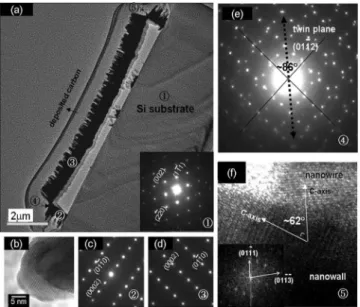
The microstructures and crystallographic orientations of the integrated nanostructures were characterized by high-resolution transmission electron microscopy共HRTEM兲. Fig-ure2共a兲shows a low-magnification TEM bright-field image of a ZnO microbox/Si共001兲 sample prepared by focused ion beam. The image shows that the nanowalls grown out of thick ZnO films are either vertical or horizontal to the Si substrate and a thin layer formed on the substrate, which should act as a seed layer for the growth of other vertical faces. Furthermore, a few nanowires and even nanowalls were grown from the seed layer. All the nanowalls are single-crystalline wurtzite structures along the ZnO 关0001兴 direc-tion, as demonstrated in Fig.2共b兲, and epitaxially grown on thick ZnO films for all faces, as evidenced in the diffraction patterns of Figs.2共c兲and2共d兲 from regions 2 and 3 in Fig.
2共a兲. This indicates that all the facets on the microboxes are the same兵0001其 planes with all the surface normal pointed to,关0001兴 suggesting that the microboxes should be formed sequentially via self-assembly rather than the commonly ob-served mechanism with surface oxidation followed by inte-rior sublimation of a single-crystalline polyhedral Zn particle,14,15 which would lead to porous microboxes
en-closed by different faceted planes. Moreover, we have shown an incomplete microbox in Fig. S1 of the supporting materi-als, clearly demonstrating an intermediate stage during the self-assembly process.
How can differently oriented ZnO sheets be assembled at the particular angles? On examining Fig.2共e兲from region 4 in Fig.2共a兲, representing a joint region connecting vertical and horizontal nanowalls, the diffraction pattern shows a twin with two sets of wurtzite single-crystal diffraction spots rotated by 86° to each other, with both along 关21¯1¯0兴 This indicates that ZnO thick films with nanowalls can be self-assembled by the twinning mechanism with 共011¯2兲 as the twin plane, by which the horizontal and vertical nanowalls in the microboxes were apparently connected to each other perpendicularly.
As for how the horizontal nanowalls connect at an ap-parent 60° to each other in a sixfold symmetric microbox, Fig.2共f兲of a high-resolution image from zone 5 in Fig.2共a兲
may represent the case, since this region contains the vertical nanowalls connected by an oblique single-crystalline nano-wire at an apparent angle of 60°, which is regarded the same as the hexagonal faces of the microbox. The figure reveals that the two materials are connected epitaxially, as repre-sented by the Fourier transform of the vertical nanowalls in the inset. After experiencing slight lattice distortion, the ep-itaxial relationship is characterized to be 兵0002其nanowires 储 兵011¯1其nanowalls and 具022¯0典nanowires 储具011¯3¯典nanowalls. This mechanism indicates that two ZnO crystals could be epitaxi-ally assembled to subtend about 62°, as in the microbox case. Consequently, ZnO crystals could be self-assembled into a 3D architecture by combining twinning and epitaxial mecha-nisms. In this case, the junction regions connecting differ-ently oriented nanowalls represent the change of crystal growth directions leading to the formation of 3D hexagonal microboxes. Based on the characterization by HRTEM, the crystallography of a microbox on Si共001兲 is summarized in Fig. S2 of the supporting materials. Notably, the关21¯1¯0兴 of the ZnO bottom film is parallel to the 关011兴 of Si and the epitaxial relationship remains equivalent even if the hexago-nal microbox rotates by 30°. The crystallography could ex-plain why the microboxes appear to align into two orienta-tions 30° to each other, which is shown in Fig. S3 of the supporting materials.
Based on the d spacings of the crystals calculated from the electron diffraction patterns in different regions of the microbox共shown in Fig. S4 of the supporting materials兲, the lattices are obviously distorted at the ZnO / Si interfaces and relaxed away from them. The d共0001兲 of the horizontal ZnO nanowalls besides the Si共001兲 is 5.03 Å, which was shrunk by 3.3% due to the lattice mismatch between ZnO 共011¯0兲 and Si共001兲, whereas the d共011¯0兲was expanded to 2.83 Å as a result of tetragonal distortion. The compressive strain of d共0001兲gradually decreases to zero and then becomes tensile strain and increases with the height of the vertical films, while the tensile strain of d共011¯0兲 behaves similarly, but in opposite direction. The significant lattice distortion and re-laxation suggest that strain plays a major role in the growth mechanism.
Therefore, the growth mechanisms of the hexagonal mi-crobox could be rationalized as follows. According to the observation of the embryos of the microboxes共shown in Fig.
FIG. 2. High-resolution TEM characterization of a microbox: 共a兲 low-magnification bright-field image with the inset showing the electron diffrac-tion of Si substrate,共b兲 high-resolution images of nanowalls, 共c兲 zone 2 of the horizontal nanowalls,共d兲 zone 3 of the vertical nanowalls, 共e兲 zone 4 of the junction region between the horizontal and vertical nanowalls, and共f兲 high-resolution image of the junction region of the vertical nanowalls with an oblique single-crystalline nanowire, with the inset showing the Fourier transform of the vertical nanowalls in zone 5.
173121-2 Wang, Liu, and Huang Appl. Phys. Lett. 89, 173121共2006兲
S1 of the supporting materials兲, the microbox was nucleated on a rugged single-crystalline hexagonal ZnO film, whose self-limited growth was induced by the accumulated elastic stress,16,17as discussed in our previous work.12Subsequently, the horizontal nanowalls formed via the stacking of the nanosheets around the sides of the hexagonal film until a critical height was reached for the strain relaxation. At the final step, the top plane with the vertical nanowalls formed to complete the microbox in order to reduce the total exposed surface area and total strain. The changes in the growth di-rections could not be attributed to the external mechanical or flow forces, since the growth directions are not in the same direction but have sixfold symmetry. To release the stress effectively, the crystal may grow with other growth habits at the junctions between the adjacent nanowalls by either twin-ning or epitaxy. The vertical nanowalls are usually nucleated on the protruded sites of a thick layer共shown in Fig. S5 of the supporting materials兲, probably because the stress relax-ation is greatest there. A schematic diagram of the proposed growth mechanisms is shown in Fig.3.
The room-temperature cathodoluminescence spectrum of the microboxes in Fig.4shows a relatively strong and sharp ultraviolet emission centered at around 377 nm and negli-gible green emission. The ultraviolet emission is attributed to the near band edge excitonic emission. The result indicates that the nanostructures possess good crystal quality with few defects.
In summary, hexagonal ZnO microboxes constructed of ZnO layers with vertical and horizontal single-crystalline nanowalls were synthesized via a self-assembled process by thermal chemical vapor deposition at a temperature of 500 ° C. It is shown that ZnO layers with nanowalls can be assembled at 86° and 62° to each other by twinning and epitaxy, respectively. The room-temperature
cathodolumines-cence spectrum of the microboxes shows a strong and sharp ultraviolet emission as well as a negligible green emission. The microboxes with nanowalls could be used in applica-tions for photocatalysts, sensors, and other fields demanding high surface-to-volume ratio. In particular, the vertical and horizontal nanowalls have potential to be applied as tem-plates for growth of vertically and horizontally aligned nano-wires for 3D nanoelectronics.
This work was supported by Research Grant No. NSC94-2120-M-006-006, National Science Council of Tai-wan.
1Z. W. Pan, Z. R. Dai, and Z. L. Wang, Science 291, 1947共2001兲. 2X. Y. Kong, Y. Ding, R. Yang, and Z. L. Wang, Science 303, 1348共2004兲. 3R. C. Wang, C. P. Liu, J. L. Huang, S.-J. Chen, Y. K. Tseng, and S.-C.
Kung, Appl. Phys. Lett. 87, 013110共2005兲.
4L. Liao, J. C. Li, D. H. Liu, C. Liu, D. F. Wang, W. Z. Song, and Q. Fu, Appl. Phys. Lett. 86, 083106共2005兲.
5R. C. Wang, C. P. Liu, J. L. Huang, and S.-J. Chen, Nanotechnology 17, 753共2006兲.
6Q. Wan, K. Yu, T. H. Wang, and C. L. Lin, Appl. Phys. Lett. 83, 2253 共2003兲.
7R. C. Wang, C. P. Liu, J. L. Huang, and S.-J. Chen, Appl. Phys. Lett. 86, 251104共2005兲.
8H. T. Ng, J. Li, M. K. Smith, P. Nguyen, A. Cassell, J. Han, and M. Meyyappan, Science 300, 1249共2003兲.
9J. Y. Lao, J. Y. Huang, D. Z. Wang, Z. F. Ren, D. Steeves, B. Kimball, and W. Porter, Appl. Phys. A: Mater. Sci. Process. 78, 539共2004兲. 10B. P. Zhang, K. Wakatsuki, N. T. Binh, Y. Segawa, and N. Usami, J. Appl.
Phys. 96, 340共2004兲.
11W. Xu, Z. Ye, L. Zhu, Y. Zeng, L. Jiang, and B. Zhao, J. Cryst. Growth
277, 490共2005兲.
12R.-C. Wang, C.-P. Liu, J.-L. Huang, and S.-J. Chen, Appl. Phys. Lett. 87, 053103共2005兲.
13Y. H. Wu, B. J. Yang, G. C. Han, B. Y. Zong, H. Q. Ni, P. Luo, T. C. Chong, T. S. Low, and Z. X. Shen, Adv. Funct. Mater. 12, 489共2002兲. 14P. X. Gao and Z. L. Wang, J. Am. Chem. Soc. 125, 11299共2003兲. 15H. J. Fan, R. Scholz, F. M. Kolb, M. Zacharias, and U. Gösele, Solid State
Commun. 130, 517共2004兲.
16J. Tersoff and F. K. Legoues, Phys. Rev. Lett. 72, 3570共1994兲. 17J. Tersoff and R. M. Tromp, Phys. Rev. Lett. 70, 2782共1993兲. FIG. 3. Schematic diagram of the proposed growth mechanisms for the ZnO
hexagonal microbox.
FIG. 4. Room-temperature cathodoluminescence spectrum of ZnO hexago-nal microboxes.
173121-3 Wang, Liu, and Huang Appl. Phys. Lett. 89, 173121共2006兲