Su-Shia Lin and Jow-Lay Huanga)
Department of Material Science and Engineering, National Cheng-Kung University, Tainan, Taiwan 701, Republic of China
(Received 17 October 2002; accepted 27 January 2003)
To ascertain how the substrate influences the quality of AlOxfilms, AlOxfilms were grown on a bare glass and a ZnO-deposited glass in this study. By applying a ZnO interlayer before the AlOxdeposition, AlOx films exhibited polycrystalline structure rather than amorphous as obtained by sputtering on a bare glass. For AlOx film on the ZnO-deposited glass, the transmission electron microscopy observation showed the coexistence of amorphous and polycrystalline structure, which reveals that the (122) plane in AlOx film is parallel to the surface of the substrate. The grains of the AlOxfilm grown on a ZnO-deposited glass comprising many small crystallites aggregated with sizes varying between 38 and 54 nm with irregular grain shapes. Besides, the ZnO interlayer with different deposition parameters had a significant effect in the diffusion interface between AlOxand ZnO. The ZnO interlayer could improve the optical transmission of AlOx films, especially when ZnO films are prepared with a high power of 200 W. Therefore, the glass / ZnO may be a good alternative substrate for producing high-quality AlOxfilms by controlling the epitaxial grain growth. The AlOxfilms grown on ZnO-deposited glasses have very good qualities in terms of crystallinity and optical properties.
I. INTRODUCTION
The most conventional oxide is the native alumina, which results from the exposure of aluminum metal to the atmosphere at room temperature. This oxide is ap-proximately 2 nm thick and is amorphous.1 Aluminum oxide thin films have been produced by a variety of physical vapor deposition techniques2such as direct cur-rent (dc) reactive sputtering,3dual-pulsed dc magnetron sputtering,4 dc s-gun sputtering,5 and radio frequency (rf ) sputtering.6 Ohring7 reported that aluminum oxide has a tendency to be amorphous when deposited as films. Schneider et al.2also reported that aluminum-oxide coat-ings are x-ray amorphous when the substrate tempera-tures are below 300 °C. However, many of the desirable properties depend on the crystalline phases of aluminum oxide,8
such as high hardness, high abrasive and corro-sion resistance,9
good thermal and chemical stability,10 and optical properties.2
In recent years there has been considerable research on the deposition of aluminum oxide films on a variety of substrates because of several applications of the oxide films11in industry. To investigate the influence of crys-tallinity, AlOx films were directly grown on both bare
glass and ZnO-deposited glass substrates in this study. ZnO film is attractive because it has a preferential growth along the c-axis, which was previously reported.12ZnO was recently found to be a good buffer layer for the growth of gallium nitride and a room-temperature lasing material.13 In this study, the ZnO layer was deposited by rf magnetron sputtering on a glass substrate. After the deposition, the metallic Al film was further de-posited on ZnO by dc magnetron sputtering. Then the Al film on ZnO-deposited glass was oxidized at 500 °C in air for 4 h. The major objective of this work was to investigate the influence of the ZnO layer on the AlOx film with respect to the crystallinity and optical properties.
II. EXPERIMENTAL
The ZnO and Al films were deposited by rf and dc magnetron sputtering on glass substrates. The targets used in this study were sintered stoichiometric ZnO (99.99% purity, ⭋3 × 0.25 in2, Target Materials Inc., Columbus, OH) and metallic Al (99.999% purity,⭋3 × 0.25 in2, Target Materials Inc.). The glass substrates [Corning 1737F (Elecmat, CA)] were ultrasonically cleaned in acetone, rinsed in deionized water, and subse-quently dried in flowing nitrogen gas before deposition.
a)
The sputtering was performed in Ar atmosphere with a target-to-substrate distance of 5 cm. A cryo-pump coupled with a rotary pump was used to achieve 1 × 10− 6 torr pressure before introducing argon gas (99.9995%, Lien Hwa Gas Co., Hsin Chu, Taiwan). The substrate temperature was measured using a thermocouple gauge and a hot cathode gauge. A ZnO layer was deposited prior to Al film deposition. The substrate was heated to 150 °C, and the chamber was back-filled with Ar, and the working pressure was maintained at 6 × 10⁻³ torr for ZnO deposition. The ZnO was deposited to a thickness of 300 nm.
After the ZnO layer was deposited, the Al film was grown on ZnO with the dc power of 40 W to the thick-ness of 60 nm. It was then oxidized in a quartz furnace at 500 °C for 4 h in air. Results were compared with those of AlOx film deposited on glass without a ZnO layer. Table I lists all the sputtering conditions for AlOx, ZnO, and ZnO/AlOxfilms.
X-ray diffraction ( XRD; Rigaku D/ MAX2500, To-kyo, Japan) was used to study the crystallinity and crystal orientation of the films. The microstructure of AlOxfilm grown on ZnO-deposited glass was examined using transmission electron microscopy ( TEM; Hitachi Model HF-2000 field emission transmission electron micro-scope, Tokyo, Japan) and selected-area diffraction (SAD) patterns. Energy-dispersive spectrometry ( EDS) was used to study the atomic composition of AlOx film grown on ZnO-deposited glass. The compositional depth profiles of the ZnO/AlOxfilms were investigated by Au-ger electron spectroscopy (VG. Microlab 310D AuAu-ger electron spectroscopy, West Sussex, United Kingdom). The cross-sectional view of the films was observed by field-emission scanning electron microscopy (FE-SEM; XL-40FEG field emission scanning electron microscope, Eindhoven, The Netherlands). The electron and hole depth profile of the ZnO/AlOx films were determined by electrochemical C-V profiler with photovoltage spec-troscopy (PN4300, Accent, Hempstead, United King-dom). The optical transmission spectra of films in the
ultravioled-visible-infrared ( UV-vis-IR ) region were re-corded by the UV spectrophotometer ( HP Hewlett Pack-ard 8452A diode array spectrophotometer, Palo Alto, CA). The film thickness was evaluated using a surface profiler (Alpha-Sep 500, TENCOR, Santa Clara, CA) and FE-SEM.
III. RESULTS AND DISCUSSION A. Analysis of depth profile
Figures 1(a) and 1(b) show the Auger depth profiles of samples C and D, respectively. The depth pro-files showed that diffusion occurred between AlOx and ZnO layers, and the diffusive thickness is approximately 30 nm, namely in region II. The Al:O and Zn:O ratios are greater than unity in both the samples, but the Zn:O ratio of sample C is higher than that of sample D. This is probably because ZnO films deposited at the low power had more interfaces between the microcrystallites where more oxygen could be trapped than those deposited at higher power.14
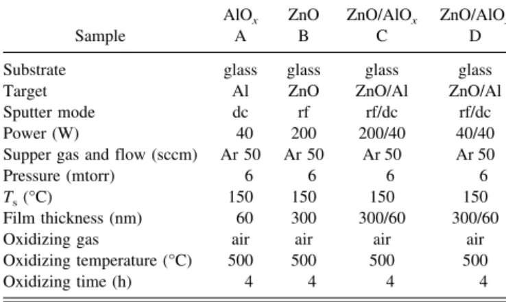
TABLE I. Sputtering conditions for AlOx, ZnO, and ZnO/AlOxfilms.
Sample AlOx A ZnO B ZnO/AlOx C ZnO/AlOx D
Substrate glass glass glass glass
Target Al ZnO ZnO/Al ZnO/Al
Sputter mode dc rf rf/dc rf/dc
Power (W) 40 200 200/40 40/40
Supper gas and flow (sccm) Ar 50 Ar 50 Ar 50 Ar 50
Pressure (mtorr) 6 6 6 6
Ts(°C) 150 150 150 150
Film thickness (nm) 60 300 300/60 300/60
Oxidizing gas air air air air
Oxidizing temperature (°C) 500 500 500 500
Oxidizing time (h) 4 4 4 4 FIG. 1. The Auger depth profiles of (a) sample C and (b) sample D,
Region II is a diffusion layer. The diffusion interface is characterized by a gradual change in composition be-tween ZnO film and AlOxfilm. The mutual solubility of ZnO and AlOx precludes the formation of interfacial compounds. Ohring15
reported that differing atomic mo-bilities may cause void formation due to the Kirkendall effect. This effect tends to weaken the interface. How-ever, the interdiffusion results in good adhesion. A re-lated type of transition zone that can strongly promote adhesion is the interfacial “pseudodiffusion” layer. The resulting condensate may be thought of as a metastable phase in which the solubility of the components involved exceeds equilibrium limits. The generally high concen-tration of point defects and structural disorder introduced by these processes greatly enhance “diffusion” between materials that do not naturally mix or adhere.
The diffusion in ZnO and AlOx can be expressed by the following equations:
2 ZnO→ Al2O3 2 ZnAl + 2 Oo+ Vo¨+ 2 e⬘ , (1) Al2O3 → ZnO 2 AlZn+ 3 Oo + VZn⬙ + 2 h˙ . (2)
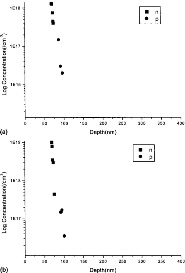
The electrons and holes in the diffusion layer were de-tected using an electrochemical C-V ( ECV ) profiler with photovoltage spectroscopy, and the results are shown in Fig. 2. The results in Fig. 2 evidence the diffusions de-scribed by Eqs. (1) and (2).
In Fig. 2, it can be seen that the concentration of elec-trons in the diffusion interface for sample D was higher than that for sample C, but the concentration of holes is almost the same. It may be due to the diffusion between AlOxand ZnO in sample D, which follows Eq. (1) when compared to sample C. In other words, Zn in sample D diffused faster than that in sample C. It indicated that the diffusion ability of Zn was greater when ZnO was prepared using the rf power of 40 W. Therefore, the ZnO interlayer indeed had a great effect in the diffusion interface between AlOx and ZnO.
The cross section of sample C was observed under SEM as shown in Fig. 3. The image is a plane view with the sample slightly tilted with the apparent illumination at the top of the micrograph. An obvious diffusion inter-face between ZnO and AlOxcan be clearly seen, and the columnar shape exists in the ZnO film.
Ohya et al.16studied ZnO film growth on a glass and reported that film crystallization was determined by the nucleation step. If the first layer was crystallized, crys-tallization of the upper, thin layer should occur epitaxi-ally. The crystals of the lower layer thus grew into the upper layer to form columnar grains surpassing the coat-ing thickness. Similarly, it is found in our study that ZnO grains grew beyond the single-coating thickness
of the film. However, the small grains were caused by the low diffusivity in the Al-doped ZnO grain and the Zn-doped AlOx grain. It has been reported that addition of Al2O3 decreases the diffusivity of ZnO by reducing the defect concentration (i.e., the interstitial Zn).17
The
FIG. 2. The electron and hole depth profiles of (a) sample C and (b) sample D, respectively.
FIG. 3. The cross section of AlOx film on ZnO-deposited glass (sample C) obtained using the SEM.
small grain size in the present ZnO films doped with Al cations also reflected this decrease in diffusivity. Therefore, the size of small grain laid across the two layers was determined by the diffusion-controlled process. B. Phase constitution
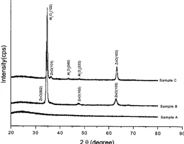
Figure 4 displays the XRD patterns of glass/AlOx (sam-ple A), glass/ZnO (sam(sam-ple B), and glass/ZnO/AlOx (sample C). It can be seen that XRD of sample A did not show any peak corresponding to the amorphous AlOxlayer. However, (122), (040), and (222) peaks from Al2O3, and (101) and (103) peaks from ZnO are visible in sample C, suggesting that AlOxfilm grown on ZnO layer was crys-talline. The ZnO layer was also deposited on the glass substrate (sample B) for comparison purpose. ZnO peaks before and after AlOx deposition do not change evi-dently. By comparing the diffraction patterns of sam-ple C with the standard Al2O3spectrum,
18
it is found that the second strongest peak (132) disappeared, and the strongest peak (122) remained. This suggests a strong (122) preferential orientation in the AlOx film due to ZnO deposition. Besides, the AlOx film exhibits an or-thorhombic structure by ZnO interlayer.
It could also be observed that ZnO film in sample B had (002) preferential orientation. Combining the strong orientation on (122) in AlOx film, we may suggest that the lattice mismatch between the averaged neighboring oxygen-oxygen distance on (122) plane of AlOx and (002) plane of ZnO, the two closest-packed planes13 is very small, and the strain energy and interface energy are also minimized.
To address issues dealing with the structure of epit-axial interfaces, Ohring19
suggested the necessity to identify the crystallographic orientation relationships be-tween the film and the substrate. The epitaxial relation-ships can be predicted on the basis of lattice-fitting
arguments. Those planes and directions that give the best lattice fit determine the orientation of the film with respect to the substrate. An important quantity that characterizes epitaxy is the lattice misfit f of the film defined as19
f =ao共s兲 − ao共 f 兲 ao共 f 兲 =
⌬ao
ao . (3)
Here, ao( f ) and ao(s) refer to the unstrained lattice pa-rameters of film and substrate, respectively. A positive f implies that the initial layers of the epitaxial film will be stretched in tension, and a negative f means that the film is in compression.
The theory predicts that any epitaxial layer having a lattice parameter mismatch with the substrate of less than about 9% would grow pseudomorphically; i.e., for very thin films the deposit would be elastically strained to have the same interatomic spacing as the substrate. The interface would, therefore, be coherent with atoms on either side lining up. With the increase in film thickness, the total elastic strain energy increases, eventually ex-ceeding the energy associated with a relaxed structure consisting of an array of so-called misfit dislocations separating wide regions of relatively good fit.
To consider the growth of a (122) plane of Al2O3 (orthorhombic crystalline) film on a (002) plane of ZnO (hexagonal crystalline) interlayer, the unit cell lattice parameters for Al2O3 and ZnO are 4.844 and 3.253 Å, respectively. The resulting epitaxial geometry is denoted by (122)Al2O3||(002)ZnO
f =ao共ZnO兲 − ao共Al2O3兲 ao共Al2O3兲
=3.253 − 4.844
4.844 = − 0.3284 The result indicated that the interface of AlOxand ZnO would, therefore, be coherent with atoms on either side lining up. The AlOxfilm will be stretched as a result of compression.
The total energy in films deposited on a substrate was the sum of three components: (i) surface energy of the film, (ii) film–substrate interfacial energy, and (iii) strain energy in the film.20,21 The film generally grew with the plane of the lowest surface free energy parallel to the substrate surface, thus minimizing the surface free en-ergy of the film.22
Films were often deposited on sub-strates that had different thermal properties from the films themselves. This could lead to strain in the films, particularly if they were deposited at elevated tempera-tures.22For the growth of all films, the total energy was minimized.22
The (002) plane of ZnO film deposited in advance favored the (122) plane of AlOx to grow, so that AlOx film also had the (122) preferred orientation direction, FIG. 4. XRD patterns of glass / AlOx(sample A), glass /ZnO (sample
which was perpendicular to the substrate. The small lat-tice mismatch between (002) plane in ZnO and (122) in AlOx was believed to be the reason for the excellent crystallinity of AlOx film.
23
A comprehensive under-standing is that the minimizations of surface energy, in-terface energy, and strain energy in surface and inin-terface could lead to the dominance of orientations.20,21
According to the kinetics of crystal growth,24 – 26 the growing faces of a crystal are parts of the free surface of the film. These crystal faces correspond to the equi-librium crystal shape and are determined by the orienta-tion of the crystal. A growth competiorienta-tion can start among the neighboring crystals in case of different orientation according to the types of their growing faces (i.e., to their orientation). The faster growing crystals will grow over the slower growing ones. This competition is termin-ated when only crystals exhibiting the same type of crys-tal faces proceed to the free surface. This competitive crystal growth represents an orientation selection among the crystals resulting in the competitive growth texture.27 On the ZnO interlayer, the nuclei are randomly ori-ented and the textures are evolutionary textures due to selection mechanisms. This selection can be related ei-ther to the competitive growth of crystals (due to the different growth rates in various crystallographic direc-tions or to the crystal face dependent segregation of in-hibitors) or to the abnormal grain growth controlled by the minimum of the surface and interface energy.27The complete coalescence of the contacting crystals is a pe-riodic process during the film growth, and beside the increase of grain size, it results also in the changes of crystal orientations due to lowering the free energy of the developing crystals. A small-grained structure (corre-sponding mainly to the nucleation density) of random orientation exists in the ZnO interlayer-near part of the AlOx film. This is a restructuring process related to the lowest interface energy.27
When the AlOxfilm becomes continuous, most of the crystals forming the polycrystalline structure have al-ready participated in a series of complete coalescence during the preceding growth stages. This means that their orientation is already in or near a preferred orientation corresponding to the minimum of interface and surface energy.27Hence, the coexistence of (122) texture of AlOx and the random orientation of ZnO was observed as shown in sample C of Fig. 4.
Compared with sample B and C, the (103) peak of ZnO shifts toward the higher diffraction angle after the AlOxdeposition. Lohmann et al.
28
studied TiB2coatings on the steel, and reported that compressive stress of the lattice in a direction parallel to the surface could affect the lattice parameter perpendicular to the surface, which correlates with the x-ray peak positions. Similarly in sample C, the lattice of AlOxin a direction parallel to the interface might suffer compressive stress. Therefore,
the ZnO interlayer could be under tensional stress, which resulted in the decrease of interplanar spacing. By fol-lowing the Bragg law29
= 2dsin , (4)
where d is interplanar spacing and is the diffraction angle, it could be understood that the decrease of inter-planar spacing resulted in the diffraction angle increas-ing, therefore, compared with sample B, the (103) peak of ZnO in sample C shifts toward the higher diffraction angle after the AlOxdeposition.
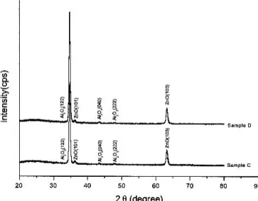
Figure 5 shows the XRD patterns of two glass/ZnO/AlOx composite films (samples C and D). The preparation con-ditions of these samples were the same except that the rf power for ZnO growth in sample C was 200 W, and in sample D was 40 W. From Fig. 5, the (122) Al2O3peak of sample D was stronger than the (122) Al2O3peak of sample C, and no peaks shifted by comparing sample C with D. This could be attributed to the fact that the ZnO films prepared at the rf power of 40 W had stronger
c-axis orientation than that prepared at the rf power of
200 W, as reported in previous work.12Besides, the re-sults indicated that there was probably lower strain en-ergy, surface enen-ergy, and interface energy in sample D. So, the plane (122) orientation of AlOx was improved effectively as compared with sample D. The ZnO inter-layer indeed affected the crystallinity of AlOx film strongly.
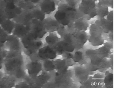
Figure 6 shows the bright-field TEM micrograph of AlOx film on ZnO-deposited glass (sample C). The TEM image showed the coexistence of amorphous and polycrystalline structures and no obvious grain bound-aries were observed. The grains were formed by many small crystallites aggregated with sizes varying between 38 and 54 nm with irregular shapes. The structure of
FIG. 5. XRD patterns of two glass / ZnO / AlOx composite films (sample C and sample D).
sample D was similar to that of sample C. The grain size of AlOx film on ZnO-deposited glass during coating could be closely related to the thickness of AlOx coat-ing. The crystal nucleation needs to reach a critical vol-ume because the increase of surface energy during crystal nucleation has to be balanced by a sufficient decrease in the lattice energy. For this reason, the crystal nucleus must be at its minimum size.30
Once an embryo exceeds the critical nucleus size, the nucleus will increase to a certain size, defined by the diffusion and/or contact of the growing grains with one another.16If the coating is much thicker than the grain size, thickness will have little effect on the grain size and shape. However, if the thickness of a single coating nearly equals or is less than the critical size of nucleus, nucleation becomes quite difficult in the film.16Therefore, the grain size and shape of AlOx film on ZnO-deposited glass were mainly affected by the film thickness. The small grain size of the AlOx film shown in Fig. 6 may be related to the thickness of coat-ing, not the deposition condition of ZnO interlayer.
Figure 7 shows the EDS analysis from the TEM study of the AlOxfilm on ZnO-deposited glass (sample C). The elements of O, Al, and Mo were found on the TEM sample surface. The small amount of Mo probably re-sulted from the TEM sample holder in the thinning proc-ess by ion milling. The results indicated that the surface shown in Fig. 6 is composed of only AlOx film. In ad-dition, the Al to O ratio was consistent with the AES results shown in Fig. 1(a). The EDS analysis of sample D also showed the similar results.
Figure 8 shows the SAD patterns from the TEM study of sample C. The SAD pattern was from AlOx and it comprised a series of rings. The SAD pattern of sample D also showed similar ring patterns. By comparing the
d-spacings of sample C (dm) with that of the standard
Al2O3 from JCPDS Card No. 88-0107 (dJCPDS), 18
the identification shows the rings corresponding to the (122), (040), (222), and (117) planes. It could be found that dm was slightly larger than dJCPDS, which suggested that the
FIG. 6. The bright-field TEM micrograph of AlOx film on ZnO-deposited glass (sample C).
Element Counts Wt % Atom %
Al 9126 75.04 64.07
O 777 24.96 35.93
Total 100.00 100.00
FIG. 7. The EDS analysis from the TEM study of the AlOxfilm on ZnO-deposited glass (sample C).
dJCPDS(Å) h k l dm(Å)
2.5806 (122) 2.6191
2.0825 (040) 2.0917
1.8965 (222) 1.9063
1.2234 (117) 1.2294
FIG. 8. The SAD pattern from the TEM study of the AlOxfilm on ZnO-deposited glass (sample C) and the values of d-spacings from JCPDS Card No. 88-010718(dJCPDS) and measured from SAD (dm).
lattice of AlOx in a direction parallel to the surface of AlOxfilm suffered compressive stress. This was consis-tent with the above discussions of XRD patterns.
The patterns in Fig. 8 suggest the coexistence of amor-phous and orthorhombic crystalline structures of AlOx because there is a gray region existing in the pattern besides a series of rings. The numerous bright spots cor-responding to the (122) plane indicates that most crys-tallites had their (122) planes in diffraction condition (i.e., nearly parallel to the electron beam).31
The TEM observation further evidenced that the (122) plane in AlOxfilm is parallel to the surface of the substrate, this was in agreement with the XRD results.
C. Optical properties
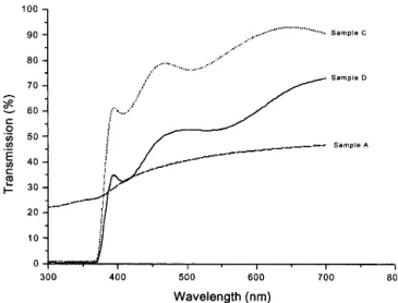
Figure 9 shows the UV-vis-IR transmission spectra of samples A, C, and D. Sample A appeared gray in color; however, samples C and D appeared yellowish and brownish, respectively. In Fig. 9 the transmission of sample A is lower than that of samples C and D. The low transmission of sample A is most probably attributed to the amorphous structure of AlOxfilm.
32
Different colors are due to the interaction between electrons and holes with photons. According to Figs. 2(a) and 2(b), the con-centration of electrons between AlOxand ZnO (region II of Fig. 1) for sample C was lower than that for sample D, resulting in the lower optical absorption for sample C.33 The transmission of sample C was higher than that of sample D (i.e., ZnO interlayer prepared at a higher power improves the optical transmission of AlOxfilm).
IV. CONCLUSIONS
By applying a ZnO interlayer before the AlOx depo-sition, AlOx films exhibited polycrystalline structure rather than amorphous as obtained by sputtering on a
bare glass. The slight lattice mismatch between (002) plane of ZnO and (122) plane of AlOxwas the reason for the excellent crystallinity of AlOx film. The ZnO inter-layer prepared at the rf power of 40 W could improve the (122) plane orientation of AlOxbecause the ZnO film at this condition had stronger c-axis orientation. For AlOx film on the ZnO-deposited glass, the TEM observation showed the coexistence of amorphous and polycrystal-line structures, and showed that the (122) plane in AlOx film is parallel to the surface of the substrate. The grain size of AlOxfilm on ZnO-deposited glass during coating could be closely related to the thickness of AlOx coat-ing and the sizes varycoat-ing between 38 and 54 nm with irregular grain shapes.
The ZnO interlayer with different deposition param-eters had a great effect on the diffusion interface between AlOx and ZnO. The low transmission is most probably attributed to the amorphous structure of AlOx film. The ZnO interlayer could improve the optical transmission of AlOx films, especially when the ZnO film was pre-pared at a high power of 200 W. The results indicate that the glass / ZnO may be a good alternative substrate for producing high-quality AlOxfilms by controlling the epi-taxial grain growth. The AlOx films grown on ZnO-deposited glass show very good qualities in terms of crystallinity and optical properties.
ACKNOWLEDGMENT
The authors would like to thank the National Science Council of the Republic of China for its financial support under Contract No. NSC-91-2216-E006-058.
REFERENCES
1. K. Wefers and C. Misra, Oxides and Hydroxides of Aluminum, Alcoa Technical Paper No. 19 (Alcoa Laboratories, Pittsburgh, PA, 1987).
2. J.M. Schneider, W.D. Sproul, R.W.J. Chia, M-S. Wong, and A. Matthews, Surf. Coat. Technol. 96, 262 (1997).
3. B. Gornachev, V. Orlinov, and V. Popova, Thin Solid Films 33, 173 (1976).
4. S. Schiller, K. Goedicke, J. Reschke, V. Kirchhoff, S. Schneider, and F. Milde, Surf. Coat. Technol. 61, 331 (1993).
5. P.J. Clarke, J. Vac. Sci. Technol. A 12, 594 (1994).
6. R. Cueff, B. Baud, J.P. Besse, and M. Jaquette, Thin Solid Films 266,198 (1995).
7. M. Ohring, The Materials Science of Thin Films (Academic Press, San Diego, CA, 1991), p. 519.
8. F. Fietzke, K. Goedicke, and W. Hempel, Surf. Coat. Technol. 86–87,657 (1996).
9. J. Skogsmo, M. Halvarsson, and S. Vuorinen, Surf. Coat. Technol. 54 / 55,186 (1992).
10. J.A. Thornton and J. Chin, Ceramic Bull. 56, 504 (1977). 11. A. Quade and H. Wulff, Thin Solid Films 355 – 356, 494 (1999). 12. S.S. Lin, J.L. Huang, and D.F. Li (2003, unpublished).
13. X.W. Sun, L.D. Wang, and H.S. Kwok, Thin Solid Films 360, 75 (2000).
14. Y.J. Kim and H.J. Kim, Mater. Lett. 41, 159 (1999).
15. M. Ohring, The Materials Science of Thin Film (Academic Press, San Diego, CA, 1991), p. 441.
FIG. 9. The UV-vis-IR transmission spectra of sample A, sample C, and sample D.
16. Y. Ohya, H. Saiki, T. Tanaka, and Y. Takahashi, J. Am. Ceram. Soc. 79, 825 (1996).
17. W. Komatsu, M. Miyamoto, S. Hujita, and Y. Moriyoshi, Yogyo Kyokaishi 76, 407 (1968).
18. JCPDS 88-0107 (Joint Committee for Powder Diffraction, Swarthmore, PA, 1999).
19. M. Ohring, The Materials Science of Thin Films (Academic Press, San Diego, CA, 1991), pp. 314 – 316.
20. C.V. Thompson, in Evolution of Surface and Thin-Film
Micro-structure, edited by H.A. Atwater, E.H. Chason, M.K. Grabow,
and M.G. Lagally (Mater. Res. Soc. Symp. Proc. 280, Pittsburgh, PA, 1992), p. 307.
21. C.V. Thompson, in Polycrystalline Thin Films: Structure,
Tex-ture, Properties and Applications, edited by K. Barmak,
M.A. Parker, J.A. Floro, R. Sinclair, and D.A. Smith (Mater. Res. Soc. Symp. Proc. 343, Pittsburgh, PA, 1994), p. 307.
22. S.V. Prasad, S.D. Walck, and J.S. Zabinski, Thin Solid Films 360, 107 (2000).
23. H.S. Kwok, X.W. Sun, and D.H. Kim, Thin Solid Films 335, 299 (1998).
24. A. van der Drift, Philips Res. Rep. 22, 267 (1967).
25. G. Knuyt, C. Quaeyhaegens, J. D’Haen, and L.M. Stals, Thin Solid Films 258, 159 (1995).
26. G. Knuyt, C. Quaeyhaegens, J. D’Haen, and L.M. Stals, Phys. Status Solidi B 195, 179 (1996).
27. P.B. Barna and M. Adamik, Thin Solid Films 317, 27 (1998). 28. R. Lohmann, E. O¨ sterschulze, K. Thoma, H. Ga¨rtner, W. Herr,
B. Matthes, E. Broszeit, and K-H. Kloos, Mater. Sci. Eng. A 139, 259 (1991).
29. B.D. Cullity, Elements of X-ray Diffraction, 2nd ed. (Addison-Wesley, Boston, MA, 1978), pp. 86 – 87.
30. J.W. Christian, The Theory of Transformation in Metals and
Al-loys, 2nd ed., Part 1 (Pergamon Press, Oxford, U.K., 1975),
p. 418.
31. D.F. Paraguay, L.W. Estrada, N.D.R. Acosta, E. Andrade, and M. Miki-Yoshida, Thin Solid Films 350, 192 (1999).
32. A. Salehi, Thin Solid Films 324, 214 (1998).
33. M. Bender, W. Seelig, C. Daube, H. Frankenberger, B. Ocker, and J. Stollenwerk, Thin Solid Films 326, 72 (1998).