References
1 CROLS, .I., and STEYAERT, M.: 'Switched-opamp: an approach to realize full CMOS switched-capacitor circuits at very low power supply voltages', IEEE J. Solid-State Circuits, 1994, pp. 936-942 2 BASCHIROTTO,A., and CASTELLO,R.: 'A 1V 1.8MHz CMOS
switched-opamp SC filter with rail-to-rail output swing'. IEEE Int. Solid-state Circuits Conf. (ISSCC97), Digest of technical papers, pp. 58-59
ed microstrip line leaky wave
roadside mainbeam
Tai-Lee C h e n
and Yu-De
LinA microstrip first hgher order leaky wave antenna (LWA), centre-fed by an aperture-coupled microstrip with a broadside mainbeam, is presented. The measured bandwidth (23% for VSWR < 21) is in agreement with the leaky radiation band predicted. The experimental gain pattems, compared with those of a patch antenna fed by the same type of structure, reveal the dfference between these two kinds of antenna. With increasing frequency, the radiation field of the LWA spreads into the H- plane, forming a flatter broadside pattern, which can be applied to long rectangular area communication.
Introduction: The leaky wave phenomenon caused by planar trans-
mission lines has recently attracted the attention of researchers and circuit designers. The advantages of wider bandwidth, fre- quency-scanning capability, relaxed tolerance for manufacturing processes etc. make the printed leaky wave antenna (LWA)
a
can- didate as an integrated device in the microwave and millimetre regimes [l]. One characteristic of the leaky travelling wave antenna is that the direction of the main beam is away from the broadside, which confines its applications. The long rectangular patch antenna with a centre microstrip feed, which is a leaky wave antenna in nature, has been investigated in [2]. However, the bandwidth is narrow and the leaky wave phenomenon is not clearly observed because the feed excites both the dominant mode and the first higher order mode of the microstrip simultaneously, and the patch length is not long enough for the travelling wave to radiate out at the end.The efficiency of the LWA hinges on its feeding structure and only appropriate feeding structures can facilitate the demonstra- tion of the intrinsic properties of the leaky mode. Unsymmetrical microstrip line [3], microstrip-to-slotline transition [4], and CPW- to-slotline transition [5] were developed to excite the microstrip line first higher order leaky mode. These feeding structures, how- ever, use either transformer or transition circuits as matching net- works that would limit the bandwidth or affect the radiation fields. Also, these feeding structures cause the main beam of the antenna to be away from the broadside direction. In this Letter, we use the aperture-coupled microstrip [6] to excite the microstrip first higher order leaky mode. Besides the advantage of avoiding interference between feeding networks and antenna radiation, no complicated matching networks or transition circuits are required. Furthermore, the position of the slot can be adjusted to achieve the desired scanning angle range, which is restricted by the inher- ent property of the LWA. As in the patterns described below, the application of the broadside LWA can be used in long rectangular areas such as corridors, tunnels, trains, traffic and toll manage- ment systems, wireless communications in buildings, etc.
, hz ,, h i ,
I I
-U- w t r
Em Fig. 1 Centre-fed aperture-coupled microstrip L W A
w = 8.5mm, L = 90mm, w, = 1.58mm, 1, = 3.9mm, w, = 0.2mm, 1, =
IO", E,, = 2.2, E, = 2.2, h, = 1.57mm, h2 = 0.508"
Design: Fig. 1 shows the top view and cross-sectional view of the aperture-coupled microstrip LWA. The first higher order mode leaky wave microstrip line is placed on the top layer and the feed- ing microstrip line on the other side of the ground plane, with a coupling aperture between them. The width of the leaky wave microstrip line depends on the desired frequency band in which the space leaky wave occurs. Spectral domain analysis, with appropriate choice of branch cuts and integration contour
[7],
is employed to determine the normalised phase and attenuation con- stants, as shown in Fig. 2. The space wave leaky region [7] is -9.5- 12.5GHz for the first higher order mode of microstrip line with w = 8.5mm, h, = 1.57 mm and E,, = 2.2. The length of the leaky microstrip line (L) is chosen to be long enough so that > 90% of the power is radiated at the end of the antenna.frequency,GHz
1534121 Fig. 2 Normalised phase and attenuation constants for leaky mode of
microstrip, and measured return losses of L W A and P A
Specification of PA: w = 8.9mm, 2L = 8.6mm, w, = 1.58mm, I, = 3.5mm, w, = 0.8mm, 1, = 5mm, E,, = 2.2, Er2 = 2.2, h, = 1.57mm, h2 = 0.508" d k , PA . . . ! $ A - - - - z 90" ..
tm
Pig. 3 Measured H-plane (x-z plane) power gain patterns of P A and L W A
- - - - 9.5GH.z LWA 9.5GHz PA
11.5GHz LWA , , . , , . . .
The slot between the two layers acts like a transformer port that couples the energy between the two layers. The size of slot deter- mines the equivalent turns ratio, which is tuned to match the real part of the input impedance of the LWA on the top layer. A 50Q
open microstrip line on the other side of the ground plane is used to excite the slot. The length of the open stub 1, is selected to be
-
one-quarter of the guided-wavelength of the feeding microstrip line, to obtain the maximum power coupling to the slot.z 90”
270”
Fig. 4 Measured E-plane (y-z plane) power gain patterns of P A and L W A
- _ - - 9.5GHz LWA
. . . 11.5GH.z LWA
~ 9.5GHz PA
Experiment results: The measured return loss of the LWA com- pared with the aperture-coupled patch antenna P A ) is also shown in Fig. 2. They are fabricated on RT-Duroid 5880 substrate with 0 . 5 0 ~ copper cladding. This shows the typical difference between the LWA and conventional resonant type antenna; the former possesses a wider bandwidth (23% for VSWR < 2:1, 9.3- 11.8GHz) which is in agreement with the predicted space-wave leaky region mentioned above, while the latter has a much nar- rower bandwidth (8.4% for VSWR < 2:1, 9.1-9.9GHz).
The measured H-plane (x-z plane) and E-plane
o/-z
plane) power gain patterns are shown in Figs. 3 and 4. The dominant polarisation is E+, where I$ is the azimuth angle on the y-z plane. At 9.5GHz, the pattern of the LWA is similar to that of the PA, except that it has a slightly narrower beamwidth in the H-plane. Because the pattern caused by half of the LWA inclines toward the end-fire as the frequency increases, the sum pattern of the radiation fields of the total strip results in the field spreading in the H-plane at 11.5GHz, as shown in Fig. 3. This characteristic can be applied to the specified broadside pattern contour of a long rectangular zone.0 IEE 1998
Electronics Letters Online No: 19980969
Tai-Lee Chen and Yu-De Lin (Institute of Communication Engineering, National Chiao Tung University, Hsinchu, Taiwan, Republic of China)
18 May 1998
References
1 OLINER, A.A., and LEE, K.s.: ‘Microstrip leaky wave strip antennas’. IEEE Int. Antennas Propagat. Symp. Dig., Philadelphia, PA, June
1986, pp. 443446
2 BHATTACHARYYA, A.K.: ‘Long rectangular patch antenna with a single feed’, ZEEE Trans. Antennas Propag., 1990, 38, pp. 987-993 3 MENZEL, w.: ‘A new traveling-wave antenna in microstrip’, Arch.
Electron. Ubertrag. tech., 1979, 33, pp. 137-140
4 LIN, Y.-D., SHEEN, LW., and TZUANG, c.-K.c.: ‘Analysis and design of feeding structures for microstrip leaky wave antenna’, ZEEE Trans. Microw. Theory Tech., 1996, MTT-44, pp. 1540-1547
5 CHOU, G.-J., and TZUANG, c.-K.C.: ‘Oscillator-type active-integrated antenna: the leaky-mode approach’, ZEEE Trans. Microw. Theory Tech., 1996, MTT-44, pp. 2265-2272
6 POZAR, D.M.: ‘Microstrip antenna aperture-coupled lo a microstripline’, Electron. Lett., 1985, 21, (2), pp. 49-50
7 LIN, Y.-D , and SHEEN, J.-w.: ‘Mode distinction and radiation- efficiency analysis of planar leaky wave line source’, ZEEE Trans. Microw. Theory Tech., 1997, MTT-45, pp. 1672-1680
ELECTRONICS LETTERS
9th
July 1998
Vol.
34
Nc
Compact low noise receiving antenna
T.D.
Ormiston,P.
G a r d n e r a n dP.S.
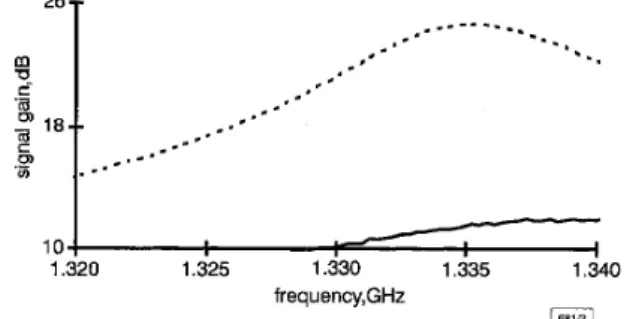
HallThe authors report a novel active integrated receiving antenna providing between 12 and 24dB gain when referred to a passive equivalent at 1.335GHz. ‘The antenna is of a compact coplanar form, integrating DC and RF requirements to obtain both high gain and low noise.
Introduction: The developmenf of active antennas that provide higher gain and low noise has been reported; examples include a half wave microstrip active antenna [l] and a printed dipole antenna [2]. These gave an increase of 8.6dB at 1.547GHz and 8.3dB at 5.8GHz above a passive equivalent with noise figures of 1.8 and 1.4dB, respectively. To our knowledge, a highly integrated compact solution in a coplanar form has not previously been achieved. A short circuit patch was chosen since the short can be used to allow the FET source leads to be easily grounded, within a quarter wave compact antenna shape. To improve the noise, it is often desirable to introduce some negative feedback [3]. In an FET-based amplifier, this is achieved by adding some inductance to the source leads [4]. This antenna topology is carefully designed so that some source inductance may be introduced onto the source leads. Thus DC, R F and low noise criteria have been satisfied in the same topology and with a much more compact and coplanar shape than any previous design. Hence, this antenna may be described as having a compact structure.
-
1.0/2.6 j68111Fig. 1 New compact antenna design
Antenna A/ antenna B dimensions in millimetres
Antenna design: The basic antenna topology is shown in Fig. 1. The active device used was a GaAs FET type ATF10136, which has a maximum stable gain of -* 23dB, and a minimum noise fig-
ure of 0.4dB at 1GHz. Two antennas were etched on TaconicTM TLY-5-0200, which has a dielectric constant of 2.2 f 0.01 and a thickness of 0.508mm. Both antennas had similar ground plane areas.
1.320 1.325 1.330 1.335 1.340
frecluency,GHz
Fig. 2 Active antenna signal gain at main lobe of A and B compared to passive
_ _ - - B active gain A active gain
Two antennas, A and B, wene constructed. The source leads of antenna A were carefully desigped to be as close to ground as