國立臺灣大學電機資訊學院電信工程學研究所 博士論文
Graduate Institute of Communication Engineering College of Electrical Engineering & Computer Science
National Taiwan University Doctoral Dissertation
背覆導體共面波導饋入開槽天線之設計
Design of Slot Antennas Fed by Conductor-Backed Coplanar Waveguide
藍逸青 I-Ching Lan
指導教授:許博文 博士 Advisor: Dr. Powen Hsu
中華民國 97 年 6 月
June, 2008
誌謝
本論文的完成,首先得感謝許博文教授長期的指導與栽培。我常覺得自己很 幸運,擁有每個研究生夢寐以求的、最高的自由度。五年的研究生生涯,我總能 自由挑選並全心全意投入自己熱愛的研究主題而毫無顧慮,這都得感謝老師全力 的支持以及完全的信任。研究的道路上,或顯或隱,更常可發現老師細心的安排。
其次我要感謝學長陳士元教授,自我是個專題生起,學長就以師長的態度引領我 熟悉天線這個領域、不辭辛勞解答我無數次的請益;擔任教職後,依然保持學長 的親切與熱心。感謝口試委員張道治教授、莊晴光教授、張知難教授、鄭士康教 授,以及鍾世忠教授,委員們的寶貴意見使本論文更臻完備。感謝胡振國教授在 我求學路上多次的推薦。
感謝王儷憲助教在大學部電磁波實驗時的指導與諸多討論,促使我對微波領 域產生更高的興趣。感謝季重儀先生傾囊相授的寶貴實驗技巧,以及維護電波組 實驗設備的良苦用心。感謝陳一仁、曾昭雄、劉安錫、賴明佑、孫瑞伯、鄧卜華、
吳昭篁、趙世峰等學長在諸方面的指導。感謝電波組92級的所有夥伴們,同窗兩 年真是愉快又難忘的回憶。尤其是同門派的一哥柏翔、賴博宗民、蔡兄書孔;共 同在博班打拼的宗男、士程;還有千哥大千、大蛇士傑,以及我的火雞好友建勳。
感謝許派的眾同學與學弟們:忠侯、昱緯、襄臨、君朋、奇軒、祐傑、如弘、舷 剛、兆祥、秉孝、彥儒、人傑、佑霖,很榮幸能與各位齊力在天線研究上努力。
感謝電波組的美女助理群:辣媽淑貞、惠美、宜芳、葦珊,有你們的照顧真幸福。
感謝電信所辦公室的趙姐文瑛、欣梅、惠玲,謝謝你們長期的幫忙。
感謝爸爸、媽媽、哥哥、姐姐、姐夫,你們無盡的愛是我一生最強韌又柔軟 的倚靠,我所以為我,皆來自於你們的愛。感謝阿公,讓您載在腳踏車後座兜風 上學的回憶仍常縈繞我心頭。感謝佳霙,未來的路我們還要一起走,如同一路走 來那般美麗與甜蜜。最後,感謝上天與大地。
逸青 2008.7.21
摘要
本論文提出了創新的背覆導體共面波導饋入之開槽天線,其中包括了三種耦 合雙開槽天線以及兩種平行板開槽陣列天線。首先介紹的是背覆導體共面波導在 開槽偶極天線這個不連續環境下產生的洩漏效應,然後藉由利用此洩漏波並適當 設計開槽偶極天線與另一平直開槽天線的耦合,天線整體的輻射表現得以增進。
接著提出的是開槽偶極天線與一弧形開槽天線的耦合結構,此一設計的天線尺寸 比前一個設計來得小巧。緊接其後的是一個藉由截斷接地面與介質基板達成微小 化的設計,其中截斷處的邊際電場扮演了耦合開槽天線在前述兩個設計中的角 色,而天線整體表現也相似。
論文下半部轉而處理均勻的背覆導體共面波導傳輸線產生的平行板模態洩漏 效應,並提出了兩種利用此洩漏波激發的平行板開槽陣列天線。為了達成線性極 化,分別設計了一個縱向陣列天線與一個橫向陣列天線,並詳敘其設計流程。而 前者優於後者之處也將在文中彰顯。這種型式的結構擁有在背覆導體共面波導基 礎下設計大型陣列天線的潛力。
Abstract
Novel slot antennas fed by the conductor-backed coplanar waveguide are proposed in this dissertation. These include three kinds of the coupled twin slots and two versions of the parallel-plate slot array. First the leakage effect at the slot dipole discontinuity of the conductor-backed coplanar waveguide is introduced. Then the slot dipole coupled with a straight slot is properly designed to utilize the leakage wave for enhanced radiation performance. Next, the slot dipole coupled with an arc-slot is presented, which is more compact than the previous design. After that, the miniaturized design with truncated ground planes and dielectric substrate is presented. The fringing fields at the truncation play the role of the coupling slot in the previous two designs. The overall performance is found to be comparable to its predecessors.
The second half of this dissertation deals with the parallel-plate mode leakage from the uniform conductor-backed coplanar waveguide. Two parallel-plate slot arrays that are excited by this leakage wave are presented. To obtain linear polarizations, a longitudinal and a transverse slot array are designed and the procedures are detailed.
The superiority of the former over the latter will also become obvious in the context.
This type of structure has the potential for large array design based on the conductor-backed coplanar waveguide.
Contents
口試委員會審定書 i
誌謝 iii
摘要 v
Abstract vii
Contents ix
List of Tables xii
List of Figures xiii
Chapter 1 Introduction 1
1.1 Motivation... 1
1.2 Literature Survey ... 1
1.3 Contribution ... 9
1.4 Chapter Outlines ... 10
Chapter 2 Coupled Twin Slots Fed by Conductor-Backed Coplanar Waveguide 14 2.1 The Straight-Slot Case... 14
2.1.1 Introduction ... 14
2.1.2 Antenna Structure and Design... 16
2.1.3 Experimental Results... 19
2.1.4 Design Procedure... 21
2.1.5 Summary... 21
2.2 The Arc-Slot Case ... 22
2.2.1 Introduction ... 22
2.2.2 Antenna Structure... 23
2.2.3 Simulation and Measurement Results ... 24
2.2.4 Design Procedure... 26
2.2.5 Summary... 26
2.3 The Miniaturized Case ... 27
2.3.1 Introduction ... 27
2.3.2 Antenna Operation... 28
2.3.3 Simulation and Measurement ... 29
2.3.4 Design Procedure... 30
2.3.5 Summary... 30
2.4 Comparison... 32
Chapter 3 Parallel-Plate Slot Array Fed by Conductor-Backed Coplanar Waveguide 57
3.1 The Longitudinal Case... 57
3.1.1 Introduction ... 58
3.1.2 Antenna Structure... 59
3.1.3 Analysis ... 61
3.1.4 Array Design and Measurement ... 66
3.1.5 Design Procedure... 69
3.1.6 Summary... 70
3.2 The Transverse Case... 71
3.2.1 Introduction ... 71
3.2.2 Antenna Structure... 71
3.2.3 Simulation and Measurement Results ... 72
3.2.4 Design Procedure………74
3.2.5 Summary... 75
Chapter 4 Conclusion 100
Appendix A Explanation of the Leakage Occurrence 103
Reference 106
Publication List of I-Ching Lan 125
List of Tables
Chapter 2
Table I Summary of the measurement results of the three designs of the coupled twin slots... 56 Chapter 3
Table II Summary of the H-plane main beam positions and antenna gains of the 5x6 array without termination ... 94 Table III Summary of the E-plane main beam positions... 99
List of Figures
Chapter 1
Fig. 1. 1 Structure of the coplanar waveguide (CPW)... 12 Fig. 1. 2 Structure of the conductor-backed coplanar waveguide (CBCPW)... 13 Chapter 2
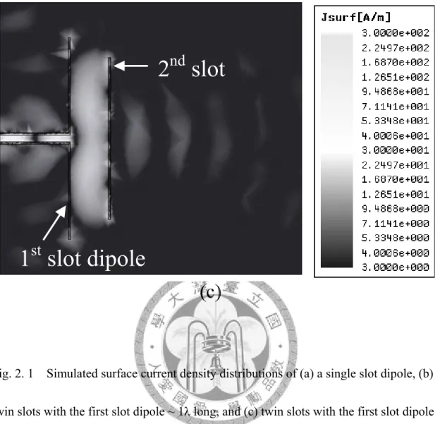
Fig. 2. 1 Simulated surface current density distributions of (a) a single slot dipole, (b) twin slots with the first slot dipole ~ 1λ long, and (c) twin slots with the first slot dipole ~ 2λ long. All cases are fed by the CBCPW with the same
dimension. ... 34 Fig. 2. 2 Geometry and photograph of the proposed CBCPW-fed slot dipole coupled
with a straight slot. ... 35 Fig. 2. 3 Simulated results for normalized L2 versus L1 with a broadside main beam at
5 GHz. S1 = 1.5 mm, Lf = 15 mm, d = 13.1 mm, W = 2.5 mm, G = 0.8 mm, h
= 1.6 mm, εr = 4.2, and tanδ = 0.02. ... 36 Fig. 2. 4 Simulated (a) radiation and antenna efficiencies and (b) antenna gain versus
L1 at 5 GHz. S1 = 1.5 mm, Lf = 15 mm, d = 13.1 mm, W = 2.5 mm, G = 0.8 mm, h = 1.6 mm, εr = 4.2, and tanδ = 0.02... 38
Fig. 2. 5 Simulated and measured input return losses and gains of the proposed antenna with L1 = 60 mm, L2 = 59 mm, S1 = 1.5 mm, S2 = 2.7 mm, d = 13.1 mm, Lf = 15 mm, W = 2.5 mm, G = 0.8 mm, h = 1.6 mm, εr = 4.2, and tanδ =
0.02. ... 39
Fig. 2. 6 Simulated and measured radiation patterns of the proposed antenna at 5 GHz. (a) E-plane (y-z plane). (b) H-plane (x-z plane)... 41
Fig. 2. 7 (a) Geometry of the proposed CBCPW-fed slot dipole coupled with an arc-slot. (b) Equivalent magnetic current on the radiating slots. (c) Photograph... 43
Fig. 2. 8 Simulations of (a) radiation efficiency and (b) antenna gain. Sd = 1 mm, Sa = 1.5 mm, Sm = 1 mm, Ld = 18.5 mm, Lm = 4 mm, and d = 15.65 mm... 45
Fig. 2. 9 Simulated and measured input return losses. ... 46
Fig. 2. 10 Simulated and measured antenna gains... 47
Fig. 2. 11 Measured radiation patterns at 5.02 GHz. (a) E-plane; (b) H-plane. ... 48
Fig. 2. 12 Measured radiation patterns at 4.9 GHz. (a) E-plane; (b) H-plane. ... 49
Fig. 2. 13 Measured radiation patterns at 5.2 GHz. (a) E-plane; (b) H-plane. ... 50
Fig. 2. 14 Geometry and photograph of the proposed CBCPW-fed finite ground slot dipole antenna... 51
Fig. 2. 15 Measured and simulated input return losses of the proposed antenna. ... 52
Fig. 2. 16 Normalized measured (a) E-plane and (b) H-plane radiation patterns at 5.0 GHz... 53 Fig. 2. 17 Normalized measured E-plane co-polarization patterns at (a) 4.8 GHz, (b)
4.9 GHz, and (c) 5.1 GHz... 55 Chapter 3
Fig. 3. 1 Geometry of the proposed antenna with a 3 x 6 longitudinal slot array. ... 76 Fig. 3. 2 Relationship between the leakage wave and the relative phases of the fields
on the slots... 77 Fig. 3. 3 Normalized leakage power from (a) different lengths of the CBCPW-line and (b) different sections within a line with a total length of 250 mm. ... 79 Fig. 3. 4 Normalized radiated power of a slot pair versus ds at 5.5 GHz. ls = 23 mm
and ws = 2 mm. ... 80 Fig. 3. 5 Normalized radiated power of a slot pair versus slot length. f = 5.5 GHz, ws = 2 mm, ds = 13 mm, and dy = 31 mm. ... 81 Fig. 3. 6 Normalized radiated power versus dt for a 5 x 2 array at 5.5 GHz. ... 82 Fig. 3. 7 Measured and simulated input return losses of the 5 x 2 array without
termination... 83 Fig. 3. 8 Measured and simulated H-plane patterns of the 5 x 2 array with and without
termination at 5.5 GHz. Solid line: measurement without termination; dotted
line: measurement with termination; cross: simulation without termination;
circle: simulation with termination... 84
Fig. 3. 9 Measured and simulated E-plane patterns of the 5 x 2 array with and without termination at 5.5 GHz. Solid line: measurement without termination; dotted line: measurement with termination; cross: simulation without termination; circle: simulation with termination... 85
Fig. 3. 10 Photograph of the 5 x 6 array... 86
Fig. 3. 11 Measured and simulated input return losses of the 5 x 6 array without termination... 87
Fig. 3. 12 Measured and simulated H-plane patterns of the 5 x 6 array without termination at 5.5 GHz. ... 88
Fig. 3. 13 Measured and simulated E-plane patterns of the 5 x 6 array without termination at 5.5 GHz. ... 89
Fig. 3. 14 H-plane patterns of the 5 x 6 array without termination. (a) 5 GHz, (b) 5.25 GHz, (c) 5.75 GHz, and (d) 6 GHz... 93
Fig. 3. 15 Geometry and photograph of the proposed transverse array... 95
Fig. 3. 16 Measured and simulated input return losses. ... 96
Fig. 3. 17 Measured and simulated radiation patterns in the y-z plane. ... 97
Fig. 3. 18 Radiation patterns in the E-plane at various frequencies. ... 98
Appendix A
Fig. A. 1 Top view of a printed strip, showing the angle of leakage θ into the surface wave of wave number ks on the surrounding dielectric substrate layer... 105
Chapter 1 Introduction
1.1 M OTIVATION
Surprises are no surprise to research works. For some researchers analyzing the modal problems of certain wave-guiding structures, the phenomenon of leaky wave radiations was discovered and evolved into a new category of powerful antennas. For some, like the author, attempting to include a conducting plane in the backside of slot antennas to obtain a unidirectional radiation pattern and perhaps higher antenna directivity and gain, the consequence is a disaster. The structure becomes overmoded and the antenna performances degrade drastically. This dissertation endeavors to seek for an elegant engineering method to improve the radiation performance of slot antennas backed by a conducting plane, especially with a coplanar waveguide feed.
1.2 L ITERATURE S URVEY
Proposed in 1969 [1], the coplanar waveguide (CPW) has become increasingly
popular nowadays because of several advantages it offers over the conventional microstrip line, such as the uniplanar structure, low radiation loss, low dispersion, ease of fabrication, and the ability of being easily integrated with active and passive devices without the need of via holes [2]. The structure of the CPW is shown in Fig. 1.1, where the gray area represents the metal plane and the white portion is the dielectric substrate.
The parameters W and S are, respectively, the strip and slot widths of the CPW, whereas h and εr are the height and the dielectric constant of the substrate, respectively.
In practical situations there are often conducting planes backing the substrate either intentionally to improve the mechanical strength and the heat-sinking capability, to render the radiation pattern unidirectional in the antenna applications, or accidentally due to the existence of nearby metal objects. Besides, in multilayered structures, while the isolation on the same layer can be achieved by placing vias, the isolation between layers is usually realized by placing conducting planes between layers [3]. The structure now becomes the conductor-backed coplanar waveguide (CBCPW), and the structure is shown in Fig. 1.2. Some examples of using the CBCPW as a feed-line can be found in [4] – [16]. Special purposes or applications such as transitions [17] – [19], measurements of complex permittivity and permeability [20], [21], or even sensors [22]
also exist.
The CBCPW is an overmoded, leaky guiding structure. In addition to the CPW
mode, the top and bottom conducting planes also support the parallel-plate mode. The originally bound CPW mode now leaks power in the form of the parallel-plate mode along a particular angle relative to the main CPW line. Since the transverse electromagnetic (TEM) wave in the parallel-plate waveguide region does not have a cut-off frequency, there will always be some power leakage in the lateral direction for all frequencies [23]. In addition, the parallel-plate mode has the same symmetry as the CPW mode and therefore cannot be suppressed by air bridges [24]. The physical idea of the leakage phenomenon was clearly explained in [25] and is adapted in Appendix A.
Early studies on the CBCPW can be traced back to the 1980s. In 1982 Shih and Itoh [26] treated the CBCPW as a mixture of a microstrip line and a coplanar waveguide and computed the dispersion relations as well as the characteristic impedance of the CBCPW. However, as pointed out by Shigesawa et al. [27], the analysis was not complete because it was done before the leakage was recognized to occur and therefore it missed the leakage effect altogether. In [27] the leakage effects on both conductor-backed slot lines and conductor-backed coplanar waveguides, with finite or infinite lateral extent of conductors, were introduced, and theoretical and experimental results of the phase and attenuation constants were compared. Chou et al. [23] explained why the attenuation constant of the CBCPW increases with frequency until it reaches a peak, after which it starts to decrease. The dimensions of the strip and slot widths
become electrically large at higher frequencies such that the fields concentrate below the center conductor of the CPW and get weaker in the slot region. Thus weaker fields are excited in the parallel-plate region. So the normalized phase constant approaches
εr and the attenuation constant decreases at higher frequencies. In other words, the CBCPW with larger values of the center strip width and the slot widths behaves more like a microstrip line rather than a coplanar waveguide. Other studies on the basic properties of the CBCPW appear in [28] and [29], which stated that the leakage rate of the CBCPW increases with reducing substrate height, same conclusion as in [30], [31].
The CBCPW in a metallic enclosure was discussed in [32]. Analysis of the asymmetric CBCPW can be found in [33], [34].
One of the main problems of an overmoded wave-guiding structure is the mode conversion at discontinuities. Jackson [31], [35] discussed both the gap end and the short end discontinuities in the finite-width conductor-backed coplanar waveguide.
Three modes are significant in the setup, namely the coplanar waveguide (CPW) mode, the coplanar microstrip (CPM) mode, and the microstrip (MS) mode. It was found that more power is coupled from the CPW mode to the CPM and the MS modes at the gap end discontinuity than at the short end one, and the coupled power decreases when either the substrate height is increased or the guide cross-sectional area is reduced.
Another problem of the CBCPW is the coupling between devices and crosstalk.
Coupling may be due to direct leakage, substrate resonances, or both [36]. Coupling between slotlines through a conductor backing was explained in [37], where Hirota and Itoh showed that the coupling was not due to the proximity effect but through the conductor backing.
Resonance of the CPW side conducting planes is another issue [38] – [47]. Excited by the leakage wave, the side conducting planes of the CPW behave like the resonator [38], [39], [44], so the energy is confined under the side planes and the transmission line performs awfully. Thorough investigations of this resonance phenomenon can be found in [39], where the resonant frequencies were predicted by both the patch-resonator model and the MSL (microstrip-like) model. Also found was that various side plane patterns did not suppress the resonance. Haydl [40] drew similar conclusions that the resonant frequencies of the CBCPW side planes are predictable by the patch antenna theory.
To deal with the leakage problem of the CBCPW and various side effects, several methods have been proposed. First, via holes that short the top and bottom conducting planes were used to suppress the parallel-plate modes [9], [12], [14], [18], [44], [45], [48] – [59]. Among these works, [44] is of particular importance, in which Haydl systematically investigated the effects of the via positions on the leakage suppression. It was found that placing the vias near the excitation region of the parallel-plate mode,
which is the gap region of the CBCPW, was superior to both random placements and shorting the periphery of the ground planes, which just shifted the resonant frequencies of the ground planes. Transmission characteristics of the CBCPW with via holes can also be found in [60]. The effect of the lateral walls, which closely spaced via holes resemble, on the propagation characteristics of the finite-width conductor-backed coplanar waveguide (FW-CBCPW) were presented in [61]. However, the use of via holes contradicts one main advantage of the CPW technology that via holes are not necessary for grounding [36]. Besides, placing via holes close to the CBCPW also affects the impedance [12].
The second approach is the non-leaky coplanar (NLC) waveguide proposed by Liu et al. [62], although this idea had already been practiced implicitly by other researchers [63] – [66]. The concept is to make the CPW mode slower than the dominant parallel-plate TEM mode by incorporating an additional dielectric layer, which has higher dielectric constant, with two possible configurations, i.e., either above or beneath the top metal layer the CPW ground resides. Usage and discussions of the NLC waveguide can be found in [67] – [74]. Although the transmission line itself is made no longer leaky by this method, coupling to the parallel-plate modes still occurs at discontinuities [24]. The structure also becomes more complicated and expensive due to the additional dielectric layer.
There are some other techniques developed to prevent the propagation of the parallel-plate mode, such as the uniplanar compact photonic-bandgap (UC-PBG) structure [75] – [77], the patterned backside metallization [36], the backside grooving [78], and the use of finite width dielectric guide with much higher dielectric constant that results in the total reflection of the leakage wave [58]. While the third and the fourth methods are obviously formidable due to the difficult dielectric processing, the second method still suffers when a conducting plane lies beneath the patterned metallization, not uncommon in power amplifier MMICs which have to be placed on a heat sink [42], and the first method involves the additional design of the bandgap structure.
The above are solutions specific to the transmission line scope. As for antenna applications, some different approaches have also been developed. The most noticeable is the phase cancellation technique, originally proposed in the 1980s to deal with the surface wave problems of printed dipoles [79] as well as slots on electrically thick dielectric substrates [80] – [84]. This technique uses twin broadside slots half a guided wavelength apart to cancel the undesired propagating power. Successful implementations of this technique for conductor-backed slots can be found in [85] – [90]. For these excellent works, the complexities always come from the feeding structures, since both slots are fed directly and separately. The number of dielectric
layers used, the number of feed points, or the accompanying bulky feeding circuits are major problems.
The second type is the aperture coupled patch antennas [4] – [6] that have the CPW feed-line and the coupling aperture on opposite sides of the substrate and an additional dielectric layer with the patch above. Although the patch antenna works fine, there are potential dangers because the leakage problem of the feed-line is not taken care of.
Besides, two dielectric layers are needed, which may not be acceptable in certain applications.
The final one is the coplanar patch antenna (CPA) which looks like a CPW-fed slot loop antenna with conductor backing [91] – [106]. So far this is, in the author’s opinion, the most elegant design of CBCPW-fed antennas due to its structural simplicity. Only one dielectric layer is used and via holes are not needed. Besides the characteristics of the antenna are similar to those of the conventional patch antenna so the design is straightforward. However, viewing the CPA as the microstrip patch antenna lacks completeness because the parallel-plate mode leakage indeed exists in the side ground regions, as evidenced by Fig. 7 of [103], which is obviously not true for the microstrip patch antenna that has no side grounds at all. In this dissertation we will use our proposed CBCPW-fed coupled twin slots to provide another point of view.
1.3 C ONTRIBUTION
This dissertation is devoted to the analysis and design of two novel types of antennas, both fed by the CBCPW. The first type is the coupled twin slots with three variants, including the slot dipole coupled with a straight slot, the slot dipole coupled with an arc-slot, and the miniaturized version. They utilize the leakage power generated at the discontinuity where the feed-line meets the slot dipole to excite an additional slot (or the fringing fields in the miniaturized case), thus forming a radiation-efficient coupled pair. These coupled twin slots are one of the simplest, if not the simplest, forms of antennas fed by the CBCPW to date.
The second type is the parallel-plate slot array. The parallel-plate mode leakage from the feeding CBCPW is intercepted by the slots on the side ground planes.
Depending on the directions of alignment of the slots with respect to the feed-line, a longitudinal array and a transverse array are designed. Wide impedance bandwidth, high directivity, high front-to-back ratio, and frequency-scanning of the main beam in one of the major plane cuts are the features of the proposed array.
The aforementioned two types are both designed with the CBCPW feed-line in its most basic form, i.e. with only one dielectric layer without any via holes. Besides, the height of the dielectric substrate doesn’t need to be a quarter guided wavelengths as in
several references [85], [87], [88], [107].
1.4 C HAPTER O UTLINES
This dissertation is organized in the sequence described below.
In Chapter 2, three versions of the coupled twin slots fed by the CBCPW are presented in order. First of all, the leakage phenomenon that occurs at the discontinuity of the CBCPW-fed slot dipole is illustrated visually. Then the CBCPW-fed slot dipole coupled with a straight slot is designed, fabricated, and experimented. Second, the CBCPW-fed slot dipole coupled with an arc-slot slot is presented. Some cautions about CBCPW-fed slot antenna designs are also discussed. The simulation and measurement results are demonstrated. Finally the miniaturized version is presented. Simulation and measurement results about the performance of the reduced-size antenna are shown. The smoother radiation patterns that prove the ground diffractions are alleviated are also presented.
In Chapter 3, two parallel-plate slot arrays are presented in order. First, the novel parallel-plate longitudinal slot array fed by the CBCPW is proposed. Design considerations about the choices of the slot orientation, the feed-line dimension, the inter-element spacing, and the slot dimensions are explained in detail. The reflected
wave from the end of the feed-line is also taken into consideration to compensate for the power tapering along the radiating apertures. A 5 x 6 and two 5 x 2 arrays with and without the feed-line termination are simulated, fabricated and tested. Next, the parallel-plate transverse slot array is presented. An array with an off-broadside main beam is designed to illustrate the basic concept and the predictable main beam position.
Then another array with a broadside main beam is designed to demonstrate the frequency-scanning property. Simulation and measurement results are presented.
Finally, conclusions are drawn in Chapter 4.
ε
rh S
W
Fig. 1. 1 Structure of the coplanar waveguide (CPW).
ε
rh S
W
Fig. 1. 2 Structure of the conductor-backed coplanar waveguide (CBCPW).
Chapter 2
Coupled Twin Slots Fed by Conductor-Backed Coplanar
Waveguide
2.1 T HE S TRAIGHT -S LOT C ASE
The coupling mechanism of the twin slots fed by the conductor-backed coplanar waveguide is investigated. The goal is to improve the antenna efficiency by using the phase cancellation technique and at the same time keep the structure as simple as possible. The leakage phenomenon is illustrated visually and the effects of the antenna parameters are examined numerically for choosing the appropriate variables. Finally the proposed antenna is fabricated and tested, showing 69.8 % of antenna efficiency.
2.1.1 I NTRODUCTION
Coplanar-waveguide-fed slot antennas are attractive due to their uniplanar structures and the ease of fabrication [2]. To render the radiation from bidirectional to
unidirectional, conducting planes are usually placed at the back of the antennas. The performance, however, suffers because the conductor-backed coplanar waveguide (CBCPW) and the conductor-backed slot are both leaky structures due to the incursion of the parallel-plate mode leakage [27]. The parallel-plate TEM mode has zero cut-off frequency, so the leakage phenomenon occurs at all frequencies. One major trend toward solving the leakage problem of conductor-backed slots is the phase cancellation technique originally proposed in the 1980s to deal with the surface wave problem of dipoles [79] as well as slots on electrically thick dielectric substrates [80] using infinitesimal elements. This technique uses twin broadside slots half a guided wavelength apart to cancel the undesired propagating power. Successful implementations of this technique for conductor-backed slots can be found in [88] and [90], where the slot lengths are 0.84 and 0.95 wavelengths long in [88] and about one wavelength long in [90]. For these excellent works, the complexities always come from the feeding structures, since both slots are fed directly and separately. Two dielectric layers and feeding circuits are used in [88], whereas two dielectric layers and two feeding ports are required in [90].
In this chapter we propose a new feeding mechanism for the twin slots configuration, of which the first slot dipole is directly fed by the CBCPW, whereas the second slot is coupled by the parallel-plate mode leakage excited at the discontinuity of
the first slot dipole. By means of this feeding method, the resulting geometry is single-layered with only one feed and without any additional feeding circuits or via holes. The simplicity and conciseness greatly enhance the usability of CBCPW-fed slot antennas for practical applications.
2.1.2 A NTENNA S TRUCTURE AND D ESIGN
The single slot dipole fed by the CBCPW acts more like a mode converter than an efficient antenna. It converts most of the power from the CBCPW mode to the parallel-plate mode, leaving the radiated power very small. The typical antenna gain is far below 0 dBi and the radiation efficiency below 10 %. Using the simulator HFSS from Ansoft, Fig. 2.1(a) illustrates this phenomenon, where the surface current density at the interface between the dielectric and the top metal layer is plotted. At the junction of the CBCPW feed-line and the slot dipole, the parallel-plate mode is strongly excited and propagates radially into the substrate region. In contrast, as Figs. 2.1(b) and (c) show, if an additional slot with suitable dimension is placed in front of the first slot dipole at a distance about half a guided wavelength of the parallel-plate mode according to the phase cancellation technique, the leakage is reduced significantly. Although the leakage suppression is not complete, the gain and the efficiency are greatly improved, as
will be shown shortly.
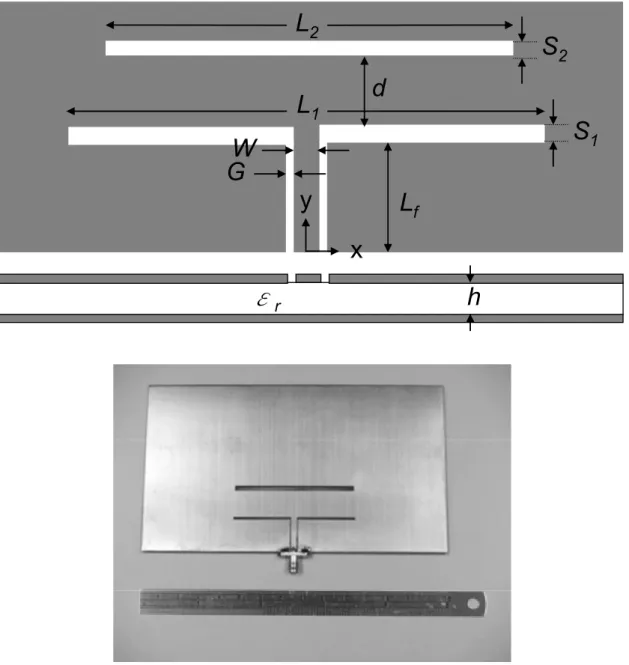
The geometry and the photograph of the proposed twin slots fed by the CBCPW are shown in Fig. 2.2. The gray area represents the metal portion and the white ones are the etched slots and the feed-line. The relative phases of the fields on the first and the second slots depend on the distance d as well as the lengths and widths of the slots, L1, L2, S1, and S2. When the distance d is half a guided wavelength of the parallel-plate mode according to the phase cancellation technique and the slots are of the same length, it is found that usually the phases are not exactly equal, resulting in an off-broadside main beam in the E-plane (y-z plane). The phases can be made equal if the slot lengths are allowed to be discrepant. Thus for each L1 value, we can find a corresponding L2
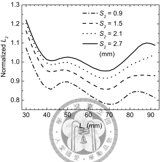
that results in a broadside main beam, assuming that the transverse dimensions (x-y plane) of the substrate and the ground are infinite so the influence of the edge diffractions on radiation patterns is temporarily ignored. The following simulations are carried out using the package software IE3D from Zeland. Fig. 2.3 illustrates the simulated results at 5 GHz, where the normalized L2 (L2 / L1) is plotted versus L1. The effect of different slot widths is also considered. From Fig. 2.3 we see that L2 might be greater than, equal to, or smaller than L1, depending on the choices of L1 and the widths of the slots. Note that since the CBCPW is a leaky line, the length of the feed-line (Lf) should not be too long. In our simulations the feed-line length is chosen to be 15 mm,
with the corresponding loss estimated to be 0.45 dB.
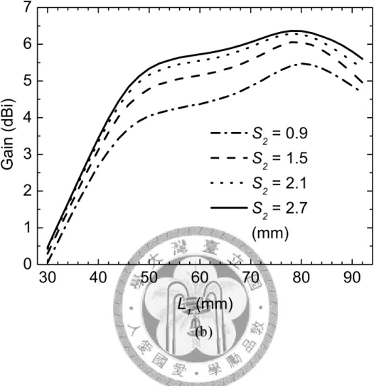
For each combination of L1 and L2 that results in a broadside main beam, the corresponding efficiencies and gains are calculated and shown in Fig. 2.4. Here the radiation efficiency is defined as the ratio between the radiated power and the input power, whereas the antenna efficiency as the ratio between the radiated power and the incident power. The difference between the incident power and the input power is the return loss at the input. Fig. 2.4(a) reveals that the radiation efficiency has local maximums when L1 is near integer multiples of λ, where λ is approximated by
2 / ) 1 (
0 / εr +
λ , which is 37.2 mm at 5 GHz for the present case. However, the serious
input mismatch makes the overall antenna efficiency below 50 % when L1 ≒ λ. On the other hand, the highest antenna gain is achieved when S2 = 2.7 mm and L1 = 78 mm ≒ 2λ, as can be seen in Fig. 2.4(b). The corresponding antenna efficiency is 64.7 % but the input return loss is just about 10 dB. If a better input matching condition is required, smaller L1 values should be chosen such that the curves of the radiation and antenna efficiencies are closer to each other. In our experiment we choose L1 = 60 mm for a better input return loss and a slightly higher antenna efficiency, although the gain is smaller due to the smaller antenna size. Note that although it seems like increasing S2
results in higher efficiencies and gains, these performances soon begin to saturate and finally fall off. Therefore in our simulations higher S2 values are not pursued further.
2.1.3 E XPERIMENTAL R ESULTS
A twin slot fed by the CBCPW is fabricated and tested with the following parameters: L1 = 60 mm, L2 = 59 mm, S1 = 1.5 mm, S2 = 2.7 mm, d = 13.1 mm, Lf = 15 mm, W = 2.5 mm, and G = 0.8 mm. The FR4 substrate with h = 1.6 mm, εr = 4.2, and tanδ = 0.02 is used in the fabrication. Note that for antenna applications, the substrate
material with lower dielectric constant and loss tangent would be more preferable.
However, in this work, the FR4 substrate was used merely because it is more accessible to us and much cheaper than other substrates. The dimensions of the substrate and the ground plane are 150 mm in the x-direction and 85 mm in the y-direction.
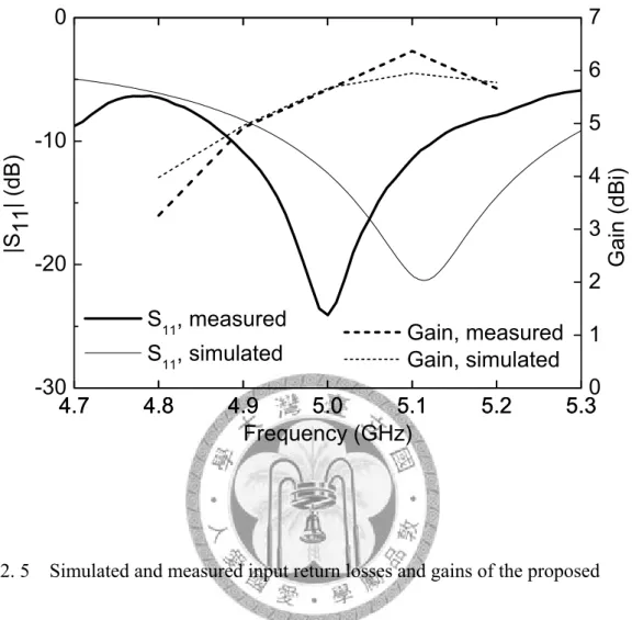
Fig. 2.5 plots the frequency response of the simulated and measured input return losses and gains. The measured input return loss is seen to have about 0.1-GHz frequency shift from the simulated one, whereas the simulated and measured gains are very close to each other. Considering that the simulation tool IE3D does not take the finite ground and the finite substrate into account and the mechanical tolerance of the fabrication process would unavoidably result in some discrepancy between the physical dimensions of the simulation model and the test piece, the results are quite satisfactory.
At 5 GHz the measured return loss is 24.1 dB and the measured gain is 5.64 dBi. The
measured 10-dB return loss bandwidth is 5 %, extending from 4.88 GHz to 5.13 GHz.
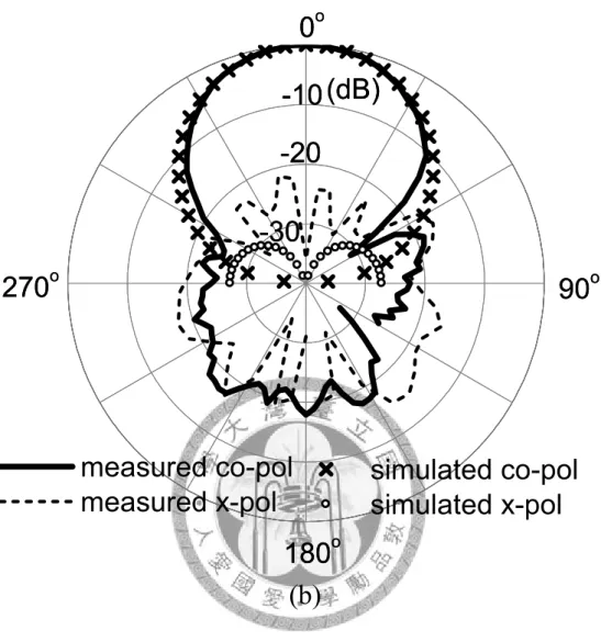
Fig. 2.6 shows both the simulated and measured E- and H-plane radiation patterns at 5 GHz. Mild ripples are observed in the measured E-plane co-polarization pattern. This is caused by the edge diffractions of the finite ground plane, which is a common phenomenon in slot antenna E-planes. The measured cross-polarization levels are fairly low in the E-plane and a bit higher in the H-plane, but are still below -15 dB in all directions. Note in Fig. 2.6(a) that the simulated cross-polarized component in the E-plane is invisible. This is because the component remains lower than -40 dB, which is the lower bound of the radial axis in the figure. The measured front-to-back ratio is higher than 17 dB.
By using the method described in [108] to estimate the directivity from the half-power beamwidths of both the E- and H-plane radiation patterns, together with the measured gain data, the antenna efficiency is found to be 69.8 % at 5 GHz. As will be shown in the next section, the antenna efficiency of the CBCPW-fed slot dipole coupled with an arc-slot is calculated using the same method, and is found to be 50.6 %.
Although the structure in the next section has the advantage of occupying a smaller area, the performance of the present structure is superior in terms of the antenna efficiency, the main concern of antennas fed by the leaky CBCPW.
2.1.4 D ESIGN P ROCEDURE
The design procedure can be summarized as follows.
1. Choose L1 ≒ 1.5 ~ 1.6 λ.
2. For d being about half the guided wavelength of the parallel-plate TEM mode, find a L2 value that is close to L1 such that the coupled twin slots have a broadside main beam in the E-plane.
3. Make S2 large enough before the antenna efficiency and gain saturate.
2.1.5 S UMMARY
The CBCPW-fed coupled twin slots have been proposed and the properties demonstrated. The coupling mechanism and the effects of the antenna parameters have been studied and utilized to design a unidirectional antenna of 69.8 % antenna efficiency with a simple structure without any complicated feeding circuits. This type of antennas would be very attractive when the CBCPW feed is unavoidable and the whole structure must be kept simple.
2.2 T HE A RC -S LOT C ASE
A novel compact slot antenna fed by the conductor-backed coplanar waveguide (CBCPW) is proposed. The antenna is composed of a CBCPW-fed slot dipole and an additional arc-slot in front of the dipole. Compared to the CBCPW-fed slot dipole without the arc-slot, the antenna gain is improved significantly. The antenna occupies a small area and uses only one layer of dielectric substrate and a single feed without any via holes. The impedance bandwidth is 7.2 % and the highest in-band antenna gain is 3.4 dBi.
2.2.1 I NTRODUCTION
In this section, we propose a new CBCPW-fed slot dipole antenna that incorporates an additional arc-slot to achieve the phase cancellation with only one layer of substrate and a single feed. The excitation of the arc-slot is through the coupling of the power leaked from the discontinuity of the feed-line, as described in the previous section. The feeding mechanism alleviates the burden of designing complicated power dividing circuits. This results in a simple geometry and a compact antenna size.
2.2.2 A NTENNA S TRUCTURE
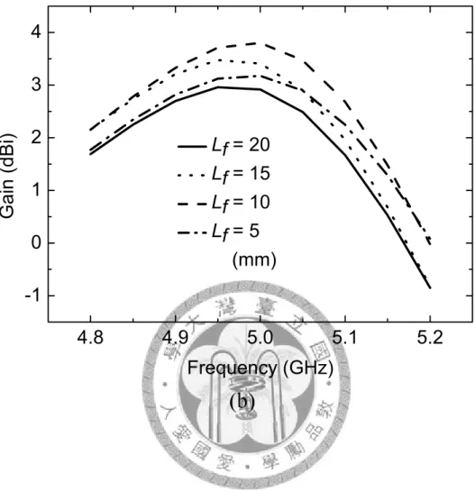
Figs. 2.7(a), (b), and (c) show the geometry of the antenna, the equivalent magnetic currents flowing on the radiating slots, and the photograph, respectively. The gray area represents the metal, whereas the white ones are the etched slots and the feed-line. As the input power travels down the feed-line and excites the slot dipole, part of the power propagates, in the parallel-plate region, toward and excites the arc-slot. When the distance d is about half the guided wavelength of the parallel-plate TEM mode, the field on the central region of the arc-slot and that on the slot dipole are in phase, which reinforces the effect of the phase cancellation. The length of the slot dipole (2 x Ld) is about λ, which is approximated by λ0 / (εr +1)/2. On the other hand, because the length of the arc-slot is fixed by its radius, two additional sections (Lm x Sm) are attached to extend the total arc-slot length to about 1.5 * λ. As opposed to the conventional transmission lines, such as the coplanar waveguide, where the feed-line length basically merely alters the phase of the input reflection coefficient, it is not true for the CBCPW-fed antennas. Since the CBCPW is a leaky line, the input power is fed directly into the antenna as well as through the coupling of the leakage power. Therefore as the feed-line length is varied, so are the amount of the coupling and hence the characteristics of the antenna. This phenomenon is best illustrated by Fig. 2.8, where the
radiation efficiency and the antenna gain simulated by IE3D from Zeland are plotted.
When the feed-line length is changed from 5 mm to 20 mm, the variation of the radiation efficiency is about 11 % at the design frequency of 5 GHz, whereas that of the gain is about 0.9 dB. Also note in these figures that the variations with frequency are not monotonic, which would be the case if there is only material loss. These two observations reveal the distinctive feature of the CBCPW and the caution that should be kept in mind when designing CBCPW-fed antennas.
2.2.3 S IMULATION AND M EASUREMENT R ESULTS
The design is based on the FR4 substrate with dielectric constant εr = 4.2, thickness h = 1.6 mm, and loss tangent tanδ = 0.02. The central distance between the arc-slot and
the dipole slot is d = 15.65 mm, which is slightly larger than one half the guided wavelength of the parallel-plate mode at 5 GHz. The remaining parameters are as follows: Sd = 1 mm, Sa = 1.5 mm, Sm = 1 mm, Ld = 18.5 mm, Lm = 4 mm, and Lf = 14 mm. The strip and slot widths of the CPW feed-line are 2 mm and 0.5 mm, respectively, which correspond to a 50-Ω characteristic impedance. Throughout the design process, simulations are carried out using the package software IE3D from Zeland.
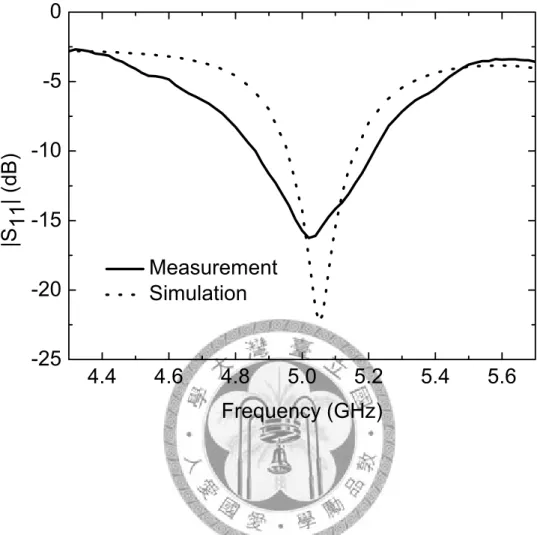
The return loss and gain are plotted in Figs. 2.9 and 2.10, respectively. The
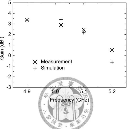
simulated resonant frequency is 5.05 GHz, whereas the measured one is 5.02 GHz. The shift in resonant frequency is less than 0.6 %. The measured bandwidth is wider than the simulated one, which may be attributed to the large loss of the dielectric substrate used in the experiment. The measured return loss at 5.02 GHz is 16.25 dB and the 10-dB return loss bandwidth is 7.2 % extending from 4.86 to 5.22 GHz. The in-band measured gain ranges from 0.55 dBi to 3.4 dBi and is 2.89 dBi at 5.02 GHz. Compared to the CBCPW-fed slot dipole without the arc-slot, which has gain far below 0 dBi, the current design increases the gain significantly, while the antenna size still kept compact.
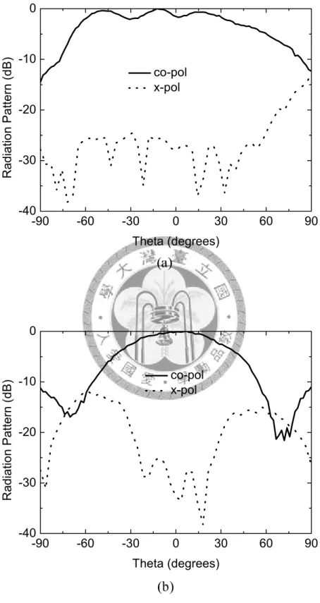
The measured radiation patterns at 5.02 GHz are shown in Fig. 2.11. The cross-polarization level in the E-plane (yz-plane) is below -20 dB except for the region near θ = 90°, which has higher levels due to the disturbance of the connecting cable in that direction. As for the H-plane (xz-plane), the cross-polarization level is higher than that in the E-plane, but still remains under -10 dB. Especially in the direction of the main beam, the level is down to below -30 dB. For comparison, the in-band patterns at 4.9 GHz and 5.2 GHz are shown in Figs. 2.12 and 2.13, respectively. As can be seen, the pattern is quite stable with respect to the frequency variations. By using the method described in [108] to estimate the directivity from the half-power beamwidths of both the E- and H-plane radiation patterns, together with the measured gain data, the antenna efficiency is found to be 50.6 % at 5.02 GHz.
2.2.4 D ESIGN P ROCEDURE
The design procedure can be summarized as follows.
1. Choose 2 * Ld ≒ λ.
2. For d being about half the guided wavelength of the parallel-plate TEM mode, attach two sections to both ends of the arc-slot to extend the total length to about 1.5 * λ.
2.2.5 S UMMARY
A novel gain-enhanced CBCPW-fed slot antenna has been proposed. An arc-slot placed in front of the slot dipole and excited by the leakage power from the CBCPW has been shown to significantly increase the gain of the slot dipole on the leaky conductor-backed structure. The measured impedance bandwidth is 7.2 %, the highest gain is 3.4 dBi in the band, and the radiation pattern is stable within the band. This antenna is useful when the compact CBCPW-fed antenna is needed.
2.3 T HE M INIATURIZED C ASE
2.3.1 I NTRODUCTION
Slot antennas fed by the conductor-backed coplanar waveguide (CBCPW) are created when there is a conducting plane, either intentionally or accidentally, lying beneath the coplanar waveguide (CPW) and the slot antenna. The conductor-backed coplanar waveguides and the conductor-backed slots are both leaky structures due to the incursion of the parallel-plate mode leakage [27]. Therefore the CBCPW-fed slot antennas usually radiate inefficiently. On the other hand, the E-plane radiation patterns of slot antennas [109], [110], similar to microstrip patches [111], usually suffer from the space-wave and surface-wave diffractions of the finite ground plane, resulting in ripples, dips, and distortions in the radiation patterns. While the problem of pattern distortion of microstrip patch antennas had been tackled in several papers [112] – [114], little had been reported for slot antennas. In this section, we propose a novel finite ground slot dipole antenna fed by the CBCPW, derived from the prototype of the CBCPW-fed coupled twin slots discussed in the first section of this chapter. By merging the finite ground diffractions with the radiating slot, the gain of the originally leaky CBCPW-fed slot dipole is increased and the radiation pattern is much smoother. The overall antenna
size is also reduced.
2.3.2 A NTENNA O PERATION
The antenna structure and the photograph are shown in Fig. 2.14. The gray and white areas represent the metal plates and the dielectric substrate, respectively. At the discontinuity where the CBCPW feed line meets the slot dipole (characterized by the size Ls x Ws), a great portion of the incident power is converted to the parallel-plate mode propagating radially away from the discontinuity. According to the investigations in the first section of this chapter, if an additional slot is placed in front of the slot dipole with suitable dimensions and distance, these twin elements will form a radiation-efficient coupled pair. In the current design, the top ground plane on which the slots are etched is truncated at the position of the additional slot such that it is replaced by the fringing field at the edge. The dielectric substrate and the bottom ground plane protrude a little for better impedance matching. The advantages the proposed structure offers are twofold. First the performance is similar to its prototype in the first section of this chapter but the current design occupies a smaller area. Second, the influence of the finite ground diffractions are overwhelmed by the fringing field radiations at the ground edge, as will be evident in the following figures that, compared to the conventional slot
antennas, the smoothness of the radiation patterns is improved and the ripple levels are much reduced.
2.3.3 S IMULATION AND M EASUREMENT
The antenna is designed and fabricated on the FR4 substrate with height h = 1.6 mm, εr = 4.35, and loss tangent tanδ = 0.02. The strip and slot widths of the 50-Ω CBCPW are S = 2.5 mm and G = 0.8 mm, respectively. The distance from the slot dipole to the ground edge is d = 15.5 mm, which corresponds to about half a guided wavelength of the parallel-plate mode at the design frequency of 5 GHz. Remaining parameters are as follows: Lf = 16.5 mm, Ls = 60.5 mm, Ws = 2 mm, Lg = 82 mm, and Wg = 42.5 mm. Ansoft HFSS was used as the simulation tool.
The measured and simulated input return losses are shown in Fig. 2.15. The measured 10-dB return loss bandwidth is 8.6 %, extending from 4.74 GHz to 5.17 GHz.
The measured results agree well with the simulated ones. The E- and H-plane radiation patterns at 5 GHz are plotted in Figs. 2.16 (a) and (b), respectively. The antenna gain at this frequency is measured to be 6.4 dBi. The E-plane co-polarization patterns at 4.8, 4.9, and 5.1 GHz are also plotted in Fig. 2.17. Note that the off-broadside main beams in some of these patterns are due to the frequency scanning property rather than the
distortions caused by ground diffractions. The patterns are seen to be much smoother than those of conventional slot antennas. This indicates that the influence of the finite ground diffractions is indeed alleviated.
2.3.4 D ESIGN P ROCEDURE
The design procedure can be summarized as follows.
1. Choose Ls ≒ λ.
2. For d being about half the guided wavelength of the parallel-plate TEM mode, protrude the dielectric substrate and the bottom ground plane a little beyond the truncation such that the input return loss becomes better.
3. Fine-tune Lg as a last resort to complete the design.
2.3.5 S UMMARY
A novel CBCPW-fed finite ground slot dipole antenna has been proposed. Using the fringing fields at one of the ground edge, the proposed antenna has been shown to provide improved gains and smoother patterns over the conventional CBCPW-fed slot antennas. This antenna is well-suited for applications of slot antennas requiring
compactness and unidirectional radiation with back conducting planes.
2.4 C OMPARISON
Three versions of the coupled twin slots fed by the CBCPW have been proposed in this chapter. The first design, the straight slot case, features impedance bandwidth of 5
%, antenna gain of 4.92 – 6.37 dBi, and antenna efficiency of 69.8 % at the center frequency. The second design, the arc-slot case, has impedance bandwidth of 7.2 %, antenna gain of 0.55 – 3.40 dBi, and antenna efficiency of 50.6 % at the center frequency. The final design, the miniaturized case, is characterized by impedance bandwidth of 8.6 %, antenna gain of 3.8 – 6.4 dBi, and antenna efficiency of 84.4 % at the center frequency. These and some additional information are summarized in Table I.
CBCPW
slot dipole
(a)
(b)
2 nd slot
1 st slot dipole
2 nd slot
1 st slot dipole
Fig. 2. 1 Simulated surface current density distributions of (a) a single slot dipole, (b) twin slots with the first slot dipole ~ 1λ long, and (c) twin slots with the first slot dipole
~ 2λ long. All cases are fed by the CBCPW with the same dimension.
L
1L
2S
1d
S
2x
y L
fh ε
rG W
Fig. 2. 2 Geometry and photograph of the proposed CBCPW-fed slot dipole coupled with a straight slot.
30 40 50 60 70 80 90 0.8
0.9 1.0 1.1 1.2 1.3
Normalized L
2L
1(mm)
S
2= 0.9 S
2= 1.5 S
2= 2.1 S
2= 2.7 (mm)
Fig. 2. 3 Simulated results for normalized L2 versus L1 with a broadside main beam at 5 GHz. S1 = 1.5 mm, Lf = 15 mm, d = 13.1 mm, W = 2.5 mm, G = 0.8 mm, h = 1.6 mm, εr = 4.2, and tanδ = 0.02.
(a)
30 40 50 60 70 80 90
20 30 40 50 60 70 80 90 100
Antenna
Efficiency (%)
L
1(mm)
S2 = 0.9 S2 = 1.5 S2 = 2.1 S2 = 2.7
S2 = 0.9 S2 = 1.5 S2 = 2.1
S2 = 2.7 (mm)
Radiation
30 40 50 60 70 80 90 0
1 2 3 4 5 6 7
Gain (dBi)
L
1(mm)
S
2= 0.9 S
2= 1.5 S
2= 2.1 S
2= 2.7 (mm)
Fig. 2. 4 Simulated (a) radiation and antenna efficiencies and (b) antenna gain versus L1 at 5 GHz. S1 = 1.5 mm, Lf = 15 mm, d = 13.1 mm, W = 2.5 mm, G = 0.8 mm, h = 1.6 mm, εr = 4.2, and tanδ = 0.02.
4.7 4.8 4.9 5.0 5.1 5.2 5.3 -30
-20 -10 0
4.7 4.8 4.9 5.0 5.1 5.2 5.30
1 2 3 4 5 6 7
|S 11| (dB)
Frequency (GHz) S11, measured
S11, simulated
Gain (dBi)
Gain, measured Gain, simulated
Fig. 2. 5 Simulated and measured input return losses and gains of the proposed
antenna with L1 = 60 mm, L2 = 59 mm, S1 = 1.5 mm, S2 = 2.7 mm, d = 13.1 mm, Lf = 15 mm, W = 2.5 mm, G = 0.8 mm, h = 1.6 mm, εr = 4.2, and tanδ = 0.02.
measured co-pol measured x-pol
(dB)
-30 -20
270
o180
o90
o0
o-10
simulated co-pol simulated x-pol (dB)
-30 -20
270
o180
o90
o0
o-10
(b) measured co-pol measured x-pol
(dB)
-30 -20
270
o180
o90
o0
o-10
simulated co-pol simulated x-pol (dB)
-30 -20
270
o180
o90
o0
o-10
Fig. 2. 6 Simulated and measured radiation patterns of the proposed antenna at 5 GHz.
(a) E-plane (y-z plane). (b) H-plane (x-z plane).
L d S d d
S a S m L m
x
y L f
ε r h
(b)
(c)
Fig. 2. 7 (a) Geometry of the proposed CBCPW-fed slot dipole coupled with an arc-slot. (b) Equivalent magnetic current on the radiating slots. (c) Photograph.
4.8 4.9 5.0 5.1 5.2 20
30 40 50 60 70
Radiation Efficiency (%)
Frequency (GHz)
Lf = 20 Lf = 15 Lf = 10 Lf = 5 (mm)
4.8 4.9 5.0 5.1 5.2 -1
0 1 2 3 4
Gai n (dBi )
Frequency (GHz) Lf = 20
Lf = 15 Lf = 10 Lf = 5 (mm)
Fig. 2. 8 Simulations of (a) radiation efficiency and (b) antenna gain. Sd = 1 mm, Sa = 1.5 mm, Sm = 1 mm, Ld = 18.5 mm, Lm = 4 mm, and d = 15.65 mm.
4.4 4.6 4.8 5.0 5.2 5.4 5.6 -25
-20 -15 -10 -5 0
|S 11| (dB)
Frequency (GHz) Measurement
Simulation
Fig. 2. 9 Simulated and measured input return losses.
4.9 5.0 5.1 5.2 -3
-2 -1 0 1 2 3 4 5
Measurement Simulation
Gain (dBi)
Frequency (GHz)
Fig. 2. 10 Simulated and measured antenna gains.
-90 -60 -30 0 30 60 90 -40
-30 -20 -10 0
Radiation Pattern (dB)
Theta (degrees) co-pol x-pol
-90 -60 -30 0 30 60 90
-40 -30 -20 -10 0
Radiation Pattern (dB)
Theta (degrees) co-pol x-pol
Fig. 2. 11 Measured radiation patterns at 5.02 GHz. (a) E-plane; (b) H-plane.
-90 -60 -30 0 30 60 90 -40
-30 -20 -10 0
Radiation Pattern (dB)
Theta (degrees) co-pol x-pol
(b)
-90 -60 -30 0 30 60 90
-40 -30 -20 -10 0
Radiation Pattern (dB)
Theta (degrees) co-pol x-pol
Fig. 2. 12 Measured radiation patterns at 4.9 GHz. (a) E-plane; (b) H-plane.
-90 -60 -30 0 30 60 90 -40
-30 -20 -10 0
Radiation Pattern (dB)
Theta (degrees) co-pol x-pol
(b)
-90 -60 -30 0 30 60 90
-40 -30 -20 -10 0
Radiation Pattern (dB)
Theta (degrees) co-pol x-pol
Fig. 2. 13 Measured radiation patterns at 5.2 GHz. (a) E-plane; (b) H-plane.
L
sW
sd
x
y L
fh ε
rG S
L
gW
gFig. 2. 14 Geometry and photograph of the proposed CBCPW-fed finite ground slot dipole antenna.
4.6 4.7 4.8 4.9 5.0 5.1 5.2 5.3 5.4 -30
-20 -10 0
|S 11| (dB)
Frequency (GHz)
Measurement Simulation
Fig. 2. 15 Measured and simulated input return losses of the proposed antenna.
co-pol x-pol (dB)
-30 -20
270o
180o
90o 0o
-10(dB)
-30 -20
270o
180o
90o 0o
-10
(b)
co-pol x-pol (dB)
-30 -20
270o
180o
90o 0o
-10(dB)
-30 -20
270o
180o
90o 0o
-10
Fig. 2. 16 Normalized measured (a) E-plane and (b) H-plane radiation patterns at 5.0 GHz.
(a)
(dB)
-30 -20
270o
180o
90o 0o
-10(dB)
-30 -20
270o
180o
90o 0o
-10
(dB)
-30 -20
270o
180o
90o 0o
-10(dB)
-30 -20
270o
180o
90o 0o
-10
(dB)
-30 -20
270o
180o
90o 0o
-10(dB)
-30 -20
270o
180o
90o 0o
-10
(c)
Fig. 2. 17 Normalized measured E-plane co-polarization patterns at (a) 4.8 GHz, (b) 4.9 GHz, and (c) 5.1 GHz.
TABLE I
SUMMARY OF THE MEASUREMENT RESULTS OF THE THREE DESIGNS OF THE COUPLED
TWIN SLOTS
Straight slot case Arc-slot case Miniaturized case
Center frequency (GHz) 5.00 5.02 5.00
10-dB return loss bandwidth (%)
5 7.2 8.6
In-band peak gains (dBi) 4.92 – 6.37 0.55 – 3.40 3.8 – 6.4 Peak gain at the center
frequency (dBi)
5.64 2.89 6.40※2
Antenna efficiency at the center frequency (%)
69.8 50.6 84.4※2
Total area of antenna plus ground plane※1 (width * length, mm)
150 * 86 150 * 104 82 * 42.5
※1: In the first and the second cases, the ground plane size may be adjusted if needed, whereas in the third case, the listed value delivers the optimum performance.
※2: The anechoic chamber at NTU Electromagnet Wave Group had been rebuilt during the summer of 2007, which was before the experiments of the miniaturized case were undertaken. Hence while the first two cases were measured in the old chamber, the third case was measured in the new one. From the author’s experience, the measured gain data of a same test piece in the old and the new chambers sometimes show variations of several decibels. So it is reasonable to assume there is some level of inaccuracy when directly comparing the gain and efficiency data of the first two cases to those of the third case.
Chapter 3
Parallel-Plate Slot Array Fed by Conductor-Backed Coplanar
Waveguide
3.1 T HE L ONGITUDINAL C ASE
The novel parallel-plate longitudinal slot array fed by the conductor-backed coplanar waveguide is proposed. Design considerations about the choices of the slot orientation, the feed-line dimension, the inter-element spacing, and the slot dimensions are explained in detail. The reflected wave from the end of the feed-line is also taken into consideration to compensate for the power tapering along the radiating apertures.
To further increase the efficiency, additional columns of slots are needed to intercept more power for radiation. A 5 x 6 and two 5 x 2 arrays with and without the feed-line termination are fabricated and tested. The measured and simulated results agree well and thus verify the design concepts. The proposed design has a broadside unidirectional pattern and is capable of frequency-scanning in the H-plane.
3.1.1 I NTRODUCTION
The coplanar waveguide (CPW) is an attractive feeding structure for planar printed antennas due to its uniplanar structure, low radiation loss, low dispersion, ease of fabrication, and the ability of being easily integrated with active and passive devices without the need of via holes [2]. In practical situations, however, there are often conducting planes backing the substrate to improve the mechanical strength and the heat-sinking capability. This turns the structure into the leaky conductor-backed coplanar waveguide (CBCPW). The originally bound CPW mode now leaks power in the form of the parallel-plate mode supported by the top and bottom conducting planes and along a particular angle relative to the main CPW line [75]. This phenomenon occurs at all frequencies and the CBCPW-fed antennas are hence inefficient radiators.
In this and the next sections, we propose a new type of slot array antenna based on the CBCPW structure that uses the parallel-plate mode leakage to radiate through the slot array etched on both sides of the ground plane of the CPW feed-line. The geometry is relatively simple and single-layered. The array design is flexible to achieve required radiation patterns. Besides, large array designs can easily be done without input-matching problems.
Compared to the transverse slot array that will be presented in the next section, the