Influence of an electric field on the optical properties of few-layer graphene with AB stacking
C. L. Lu,1C. P. Chang,2,5,*Y. C. Huang,1,3R. B. Chen,4and M. L. Lin1,5,†
1Department of Physics, National Cheng Kung University, 701 Tainan, Taiwan
2Center for General Education, Tainan Woman’s College of Arts and Technology, 710 Tainan, Taiwan
3Center for General Education, Kao Yuan University of Technology, 821 Kaohsiung, Taiwan
4Center for General Education, National Kaohsiung Marine University, 830 Kaohsiung, Taiwan
5National Center for Theoretical Sciences, Taiwan
共Received 3 November 2005; revised manuscript received 26 January 2006; published 24 April 2006兲
The effect of perpendicular electric field共F兲 on optical properties of the AB-stacked few-layer graphene, made up of two, three, or four graphite sheets, is explored through the gradient approximation. In contrast to the featureless optical spectra of graphene, the low-energy absorption spectra of few-layer graphene with AB stacking exhibit many jumping structures, which result from the band-edge states caused by the stacking effect, in the absence of an electric field. Remarkably, F causes the subband 共anti兲crossing, changes the subband spacing, produces the oscillating bands, and increases the band-edge states. It, therefore, follows that the field-modulating spectra with sharp peaks are generated. Moreover, the frequency of peak, which is strongly dependent on the layer number and the field strength, is predicted. Above all, the predicted absorption spectra and the associated electronic properties could be verified by the optical measurements.
DOI:10.1103/PhysRevB.73.144427 PACS number共s兲: 73.20.At, 73.61.⫺r, 78.20.⫺e
I. INTRODUCTION
The layered graphites have attracted a lot of studies, mainly owing to the special geometric structures.1They ex- hibit very rich physical properties, e.g., electronic properties and optical excitations. The main features of electronic struc- tures are directly reflected in optical properties. Graphite crystals are the arrangement of hexagonal graphite sheets, held by the van der Walls forces, in the AA, AB, or ABC sequence along the z axis. In general, natural graphite adopts an AB-stacking sequence.2–4Graphite sheet共graphene兲 is an atomic monolayer composed of the hexagonal rings of car- bon atoms with strongbonds. The pzorbitals, perpendicu- lar to graphite plane, cause the special electronic proper- ties—two linear energy dispersions touching each other at the Fermi energy共EF兲. A graphite sheet is a zero-gap semi- conductor with the vanishing density of state共DOS兲 at EF. Due to the geometric structure and the interlayer interactions, the AB-stacked graphite show anisotropic energy dispersions along the stack direction. The interlayer interactions mark- edly change the energy dispersions at low energy1–7and lead to the nonvanishing value of DOS at EF.
Because of the progress of fabrication technology, various graphite-based materials, such as one-dimensional 共1D兲 nanotubes,8 0D carbon toroids,9 1D nanographite mono- ribbon,10 and 2D nanographite multiribbons,11,12 are pro- duced. 1D nanotubes can be obtained from the rolling of a graphite sheet to a cylinder shape. By segmenting a long nanotube, a finite nanotube forms. A 0D carbon toroid is the connection of two ends of finite 1D nanotube in the ring form. In contrast to these tubular systems, 2D nanographite multiribbons共1D nanographite monoribbon兲 can be regarded as the slit of a graphite crystal共graphite sheet兲. By reducing the dimensionality in the graphite basal planes, such planar systems come about. Through the change in the dimension- ality and the size of materials, the peculiar electronic prop-
erties of these tubular and planar systems emerge. The find- ings are, therefore, triggering more ideas. Another option is to reduce the dimensionality of graphite along the c axis.
More recently, the stack of finite layers of graphene along the c axis, namely, few-layer graphene共FLG兲, is produced, for example, through the exfoliation of the small mesa of highly oriented pyrolytic graphite.13The experimental measurement shows that FLG is stable under ambient conditions and that FLG is a 2D semimetal with a light overlap between valence bands and conduction bands.13 The FLG has also been used to fabricate the device such as the field effect transistor.13–16 It is well known that the electric field can effectively modify both electronic and transport properties of low- dimensional systems, e.g., 1D quantum wires,17and 1D car- bon nanotubes.18–22 The influence of electric field on the physical properties of the quasi-two-dimensional FLG is to be expected. In a previous work of ours,23the dependence of electronic properties on the geometric structure共the number of layers and the interlayer interactions兲 and the electric field is investigated in detail. First, it is found that the interlayer interactions destroy symmetry and isotropy of energy bands and change linear bands into parabolic bands. They also re- markably cause the weak overlap between valence and con- duction bands in bilayer共four-layer兲 graphene. Then, the per- pendicular electric field can give rise to the subbands 共anti兲crossing, change the subband spacing, induce the oscil- lating bands, and increase the band-edge states. Remarkably, bilayer graphene makes a transition from semimetal to semi- conductor with a band gap significantly modulated by the electric field. More importantly, the effects caused by geo- metric structure and electric field—the induction of two kinds of special structures, the shift of peak position, the change of peak height, and the alternation of band gap—are revealed in DOS.
Above all, the calculation of optical properties makes it possible for us to investigate the aforementioned electronic properties. The spectroscopy24could be used to examine the
1098-0121/2006/73共14兲/144427共7兲/$23.00 144427-1 ©2006 The American Physical Society
calculated absorption spectra, which respond directly to the main features of electronic structures. By employing the gra- dient approximation, the optical properties of FLG with layer number N = 2, 3, and 4 are explored in this work. This paper is organized as follows. In Sec. II, the analytic Hamiltonian matrix elements of the tight-binding method for electronic properties of FLG are first derived. The effects of geometric structure and electric field on the low-energy absorption spectra are then investigated in Sec. III. Finally, conclusions are drawn in Sec. IV.
II. THEORY AND METHOD
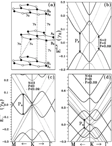
Figure 1共a兲 exhibits the geometrical structure and all tight-binding parameters of AB-stacked graphite, where two atoms, denoted as Ai and Bi, exist in the primitive cell of each graphene. In the AB order, half of atoms共Ai兲 lie directly above each other in the adjacent sheets and the other half 共Bi兲 lie above the center of the hexagons in the adjacent layers. The C-C bond length in the graphite plane is b
= 1.42 Å. The distance between the two nearest neighboring sheets is c = 3.35 Å.2The tight-binding parameters shown in Fig. 1 are as follows. That between A and B atoms on the same graphite layer is ␥0. The interaction between two A atoms from two neighboring layers is␥1. That between two B atoms from two neighboring layers is␥3.␥4represents the interaction between atom A and B from two neighboring lay- ers. The hopping integral␥5is the interaction between two A atoms from the two next-neighboring planes.␥2is the inter- action between two B atoms from the two next-neighboring planes. The atoms A form the linear atom chains along the stacking direction, while the atoms B form the zigzag tex- tures along that direction. Therefore, the second neighboring interaction ␥5 is different from ␥2. Moreover, the local chemical environment of atom A is dissimilar to that of atom B. The different chemical environment between atom A and atom B is reflected in the site energy␥6. The values of␥0and
␥i’s are2 ␥0= 2.598 eV, ␥1= 0.364 eV, ␥2= −0.014 eV, ␥3
= 0.319 eV, ␥4= 0.177 eV, ␥5= 0.036 eV, and ␥6= −0.026 eV. The AB stacked N-layer graphene can be looked upon as the extraction of the AB-stacked graphite. From this point of view, Fig. 1共a兲 also represents the geometrical structure of trilayer graphene. 2N atoms 共A1, B1, A2, B2, . . . , AN, BN兲 are found in the unit cell of the N-layer graphene with AB stack- ing. For simplicity, all the tight-binding parameters of the AB-stacked graphite are directly used to simulate these FLG systems.
An electric field 共F兲 perpendicular to graphite planes is used to modulate the electronic states of an FLG. For the sake of calculation convenience, F is assumed not to affect the rigid structure and, thus, not the tight-binding parameters of the FLG. The 2pz orbitals are fully to describe the
-electronic states that exactly dominate the low-energy electronic properties. Thebands are omitted because they are far apart from the Fermi energy. Because of the screening effect,25,26 F is an effective field, which is only to add an electric potential U = −eFz on the site energy of a carbon atom. The Hamiltonian equation is
H兩⌿典 = E兩⌿典, 共1兲
where兩⌿典 is the wave function, which is presented as the linear combination of the Bloch function 兩A典 and 兩B典. In bracket notation, the wave function is
兩⌿典 = a1兩A1典 + b1兩B1典 + a2兩A2典 + ¯ + aN兩AN典 + bN兩BN典.
共2兲 Within the frame of tight-binding method兩Ai典 and 兩Bi典, the Bloch functions for thebands at the ith graphite sheet are expressed by a linear combination of the atomic 2Pzorbitals
共RI− r −␣兲:
兩␣i典 =兺R
I
eik·RI共RI− r −␣兲, 共3兲
where ␣ denotes A or B. RI is the 3D periodical position vector and A and B are position vectors in a basis. The representation of Hamiltonian operator is a 2N⫻2N Hermit- ian matrix. Its elements are in the form of具␣i兩H兩j典, where
␣ 共兲 denotes 兩A典 or 兩B典 and i 共j兲 indicates the graphene FIG. 1.共a兲 The geometric structure of the trilayer graphene.␥0
is the intralayer interaction and␥i’s indicate the interlayer interac- tions. The light共heavy兲 curves in 共b兲, 共c兲, and 共d兲, respectively, exhibit the energy dispersions of the bilayer, trilayer, and four-layer graphene in the absence共presence兲 of electric field with the unit of
␥0/共eÅ兲. The ranges of wave number along the KM and K⌫ direc- tions are, respectively, 0.1 Kmax in 共b兲, 0.09 Kmax in 共c兲, and 0.15 Kmaxin共d兲, where Kmaxis the magnitude of wave vector point- ing from the point K to the point⌫ of the first Brillouin zone.
order 1 , 2 , 3 , . . . , N along the z axis共the stacking direction兲.
The nonzero elements are listed as follows:
具Ai兩H兩Ai典 = − eFzi+␥6,
具Ai兩H兩Bi典 =␥0f共kx,ky兲,
具Bi兩H兩Ai典 =␥0f*共kx,ky兲,
具Bi兩H兩Bi典 = − eFzi, if i is odd. 共4兲 They are also the elements of Hamiltonian matrix of the ith graphite sheet along the z axis when i is odd. Here f共kx, ky兲
=兺l=13 exp共ik·bl兲, where blrepresents the nearest neighbor in the same graphite plane and k =共kx, ky兲 is the wave vector.
The effective electric field chiefly adds an electric potential
−eFzi to the site energy of carbon atoms, where zi is the z coordinate of the ith graphite plane and is equal to zi=共i
− 1兲c. It should be noted that due to the stacking effect the elements of Hamiltonian matrix of the other half graphite sheets are
具Ai兩H兩Ai典 = − eFzi+␥6,
具Ai兩H兩Bi典 =␥0f*共kx,ky兲,
具Bi兩H兩Ai典 =␥0f共kx,ky兲,
具Bi兩H兩Bi典 = − eFzi, if i is even.
The interlayer interactions between the two nearest-neighbor graphite sheets brings about the nonzero matrix elements
具Ai兩H兩Ai+1典 = 具Ai+1兩H兩Ai典 =␥1,
具Ai兩H兩Bi+1典 = 具Bi+1兩H兩Ai典*=␥4f*共kx,ky兲,
具Bi兩H兩Ai+1典 = 具Ai+1兩H兩Bi典*=␥4f*共kx,ky兲,
具Bi兩H兩Bi+1典 = 具Bi+1兩H兩Bi典*=␥3f共kx,ky兲. 共5兲 The matrix elements resulting from the second-neighbor in- teractions␥5 and␥2are
具Ai兩H兩Ai+2典 = 具Ai+2兩H兩Ai典 =␥5,
具Bi兩H兩Bi+2典 = 具Bi+2兩H兩Bi典 =␥2. 共6兲 Energy dispersions Eh共kx, ky兲 in units of ␥0 and the related wave functions兩⌿h共kx, ky兲典 are obtained through the diago- nalization of Hamiltonian matrix, where h = c共or h=v兲 and c 共v兲 represents the unoccupied 共occupied兲 states. Further- more, the optical absorption function of an FLG is directly obtained through
A共兲 ⬀ 兺
h,h⬘,J,J⬘冕1stBZ
dkx
2 dky
2
⫻
冏
具⌿h⬘共kx,ky,J⬘
兲兩Eˆ · Pmeជ兩⌿h共kx,ky,J兲典
冏
2⫻ Im
冋
Ehf⬘关E共khx⬘,k共kyx,J,k⬘
y兲 − E,J⬘
兲兴 − f关Eh共kx,kyh,J兲 −共kx,ky,J兲兴− i⌫册
,共7兲 where f关Eh共kx, ky, J兲兴 is the Fermi-Dirac distribution func- tion.⌫ 共=0.001␥0兲 is the broadening parameter due to vari- ous deexcitation mechanism. For the sake of convenience, the subbands away from EF are assigned to be the index J
= ± 1 , ± 2 , . . . , ± N, respectively. Here + 共−兲 corresponds to the unoccupied*states共the occupiedstates兲. Electrons in the presence of electromagnetic field with Eˆ
x储xˆ 共Eˆy储yˆ兲 are excited from the occupied bands to the unoccupied * bands. At T = 0, only inter--band excitations occur. The ex- citation energy is ex= Ec共kx, ky兲−Ev共kx, ky兲. The optical se- lection rules are⌬kx= 0 and⌬ky= 0 because the momentum of photons is almost equal to zero.
具⌿共kx,ky,J
⬘
兲兩Eˆ · Pជme 兩⌿共kx,ky,J兲典,
the velocity matrix element, is evaluated within the gradient approximation27–30共Appendix A兲. The joint density of states is obtained by setting the velocity matrix element in Eq.共7兲 to 1. Apparently, the optical properties are sensitive to the electronic properties of FLG, which are greatly affected by the layer number, the interlayer interactions and the electric field.
III. OPTICAL PROPERTIES
First, the electronic properties of FLGs with layer number N = 2, 3, and 4 are briefly reviewed.23As shown by the light curves in Figs. 1共b兲–1共d兲, the band features in the absence of an electric field are quite dissimilar to those of graphene, which exhibits two linear bands crossing each other at EF. The occupied bands are asymmetric to the unoccupied bands about EF. The band features are very sensitive to the layer number. The bilayer graphene presents four parabolic bands with band-edge states close to the K point共the corner of the first BZ兲. Moreover, the valence bands slightly touch the conduction bands关Fig. 1共b兲兴. The low-energy dispersions of trilayer graphene exhibit the parabolic bands and the weak oscillating bands near EF关Fig. 1共c兲兴. At the K point, the state energies near EFare E = 0, ±␥2, and␥6−␥5. It is clearly seen that the second-neighbor interactions between the first and the third graphite planes␥2 and␥5 dominate the state ener- gies at K. The oscillating energy dispersions appear near the K point. Notably, a band gap Eg, the energy space between the band edge of J = −1 subband and that of J = 1 subband, is opened. Thus, the trilayer graphene is a semiconductor. Four- layer graphene presents the parabolic bands关Fig. 1共d兲兴. The state energies closest to E = 0 are doubly degenerate at the K
point. The energy spacing between the two degenerate en- ergy levels is equal to 2␥2. Around the K point, the state degeneracy is just destroyed. The valence bands lightly con- tact the conduction bands. Thus, the four-layer graphene is a 2D semimetal. In short, the interlayer interactions cause asymmetry between the occupied states Ev and the unoccu- pied states Ec, destroy isotropy of energy bands, change lin- ear bands into parabolic bands, and also remarkably cause weak overlap between the valence and the conduction bands.
The effective electric field leads to the significant changes in energy dispersions, as shown by the heavy curves in Figs.
1共b兲–1共d兲. It is noted that the Fermi level 共EF兲 of the systems in the presence of electric field is set at the zero energy. The perpendicular electric field F, in units of␥0/共eÅ兲, can open a band gap, cause the subband 共anti兲crossing, alter the band feature, change the band spacing, and produce new band- edge states as well. First, the electric field not only changes the parabolic bands into the oscillating bands but also in- duces a band gap in the bilayer graphene关the heavy curves in Fig. 1共b兲兴. That is to say, the semimetal-semiconductor transition occurs. In contrast to the bilayer graphene, the os- cillating bands of trilayer graphene, caused by F, cross共an- ticross兲 each other at the certain wave vector along the KM 共K⌫兲 关the heavy curves in Fig. 1共c兲兴. The electric field in- duces the semiconductor-metal transition in the trilayer graphene. The features of oscillating bands—the period and the amplitude—are very sensitive to the layer number关Figs.
1共c兲 and 1共d兲兴. Above all, the cooperation between electric field and geometric structures causes the oscillating bands and, thus, produces the new band-edge states near EF. It is expected that the characteristics of energy dispersions 共the oscillating band dispersions and the band-edge states兲 will reflect on absorption spectra of FLG.
The possible transition channels are all revealed in the features of joint density of states共JDOS兲. In the absence of electric field, JDOS of FLG with N = 2, 3, and 4 increases from = 0 to = 0.5␥0 关Fig. 2共a兲兴 due to the logarithmic peak at ⬇2␥0, which originates in the transition from band near −␥0 to* band near ␥0.23,31,32The magnitude of JDOS is in proportion to N⫻N, the possibility of transition channels. JDOS follows a similar trend as seen in the graph- ite sheet and the AB-stacked graphite. However, JDOS of FLG exhibits many special jumping structures, which are related to the local minima 共or maxima兲 in energy disper- sions 关the light curves in Figs. 1共b兲–1共d兲兴. Such jumping structures do not appear in JDOS of a graphite sheet. The chief cause is that the graphene presents two linear bands resulting in featureless JDOS near EF.
JDOS near EF关the inset in Fig. 2共a兲兴 merits a closer study.
They are related to the electronic properties, which are strongly dependent on the geometrical structure. The loga- rithmic peak of bilayer graphene originates in the saddle point in the energy dispersions. The sharp peak of trilayer graphene results from the nearly flat bands near EF. The peak position is equal to the band gap Egof the system关the light curves in Fig. 1共c兲兴. However, the four-layer graphene exhib- its quite dissimilar low-energy JDOS, which only show the oscillating feature. There is no sharp peak or band gap.
The absorption spectra A共兲 关Fig. 2共b兲兴 are calculated through A共兲=共Ax+ Ay兲/2, i.e., the average of Ax and Ay,
which are absorption spectra in the application of polarized field Eˆ
x储xˆ and Eˆy储yˆ, respectively. In the absence of perpen- dicular electric field, A共兲 grow from= 0 to= 0.5␥0. The feature of spectra is very similar to that of corresponding JDOS, and is proportional to JDOS as well. Spectra chiefly exhibit several discontinuities共or jumping structures兲. How- ever, the number of discontinuities is less than that of JDOS because the inclusion of velocity matrix closes some transi- tion channels. The inset in Fig. 2共b兲 shows that the spectra near EFare similar in structure to JDOS.
The effective electric field alters the aspects of JDOS and induces the striking peaks in JDOS共Fig. 3兲. The chief cause is that F significantly modifies the low-energy dispersions, e.g., the change of the band spacing, the alternation of the band feature, the production of oscillating band, and the gen- eration of new band-edge states. In other words, the applica- tion of F leads to the new excitation channels and, therefore, gives rise to these peaks. JDOS of bilayer graphene 关Fig.
3共a兲兴 shows that a band gap, whose size varies with field strength, is opened. The first共second兲 peak 关Pf共Ps兲兴 in the form of logarithmic共asymmetric兲 divergence is related to the saddle point共the band-edge states at the K point兲 in the en- ergy dispersions关the solid curves in Fig. 2共b兲兴. However, no band gap is found in the tri-共four-兲layer graphene. Addition- ally, these two systems exhibit JDOS with similar features FIG. 2.共a兲 Joint density of states of the N-layer graphene in the absence of an effective electric field are exhibited for N = 2, 3, and 4, respectively. The corresponding absorption spectra are shown in 共b兲.
displayed in the presence of strong field, e.g., F = 0.06 and 0.09.
The electric field F has a great effect on the absorption spectra. First, F not only opens a band gap but also induces a sharp peak in the low-energy spectra of bilayer graphene 关Fig. 4共a兲兴. The feature of absorption spectra in the energy region from = 0 to 0.2␥0 is in proportion to JDOS 关Figs.
2共a兲 and 3共a兲兴. In the application of strong field, however, spectra are featureless in the energy region 艌0.3␥0 be- cause some transition channels in JDOS 关Fig. 2共a兲兴 are closed by the vanishing of velocity matrix. In the presence of F, the steep rise of the spectra, due to the transition between the band-edge states of J = −1 and that of J = 1 subband关the dashed arrow in Fig. 1共b兲兴, can be used to determine the size of energy gap Eg. The first peak 共Pf兲, made up of two sub- peaks, is a compound one. The transition channels of these two subpeaks are indicated, respectively, by the dashed and the solid arrows in Fig. 1共b兲. The former transition produces a shoulder on the low energy side of the first peak. Hence, the main peak resulting from the saddle point in energy dis- persions is in the logarithmic form. The frequency of the first peak Pf depends on the field strength. The second peak共Ps兲 comes from the transition from local minimum of J = −1 sub- band to band-edge state of J = 2 subband on the K point关Fig.
1共b兲兴. This peak makes a blueshift in the increasing of field strength.
The absorption spectra also depend on the layer number.
The comparison between Figs. 4共b兲 and 3共b兲 shows that spectra of the trilayer graphene at艌0.2␥0are proportional to the related JDOS, i.e., these transition channels survive in the presence of F. However, the spectra at 艋0.2␥0, con- siderably modified by dipole matrix element, are dissimilar to the corresponding JDOS. Owing to the effect caused by the geometric structure, spectra of trilayer graphene 关Fig.
4共b兲兴 are quite different from those of bilayer graphene 关Fig.
4共a兲兴. No energy gap is found in the former spectra, in which Pf, close to zero, is in the form of logarithmic divergence.
The peak position is affected by the field strength and␥2, the interaction from the two next-neighboring planes. Moreover, in the presence of the strong field, a sharp peak exists at 艌0.2␥0 in the spectra of trilayer graphene.
Remarkably, the characteristics of spectra of bilayer or trilayer graphene are also found in those of the four-layer graphene. For example, the sharp peak at艌0.2␥0exists in both four-layer and trilayer graphene 关the heavy solid 共dashed兲 curves in Figs. 4共c兲 and 4共b兲兴 in the application of strong field, e.g., F = 0.09. It should be noticed that Psof the four-layer graphene关Fig. 4共c兲兴 is similar to Pfof the bilayer graphene关Fig. 4共a兲兴. Seemingly, the second peak Psis also in the logarithmic form. In addition, the frequency of Pf in the spectra of four-layer graphene is almost not affected by the strong field关Fig. 4共c兲兴. The chief cause for such a result FIG. 3. The light, dashed, heavy, and heavy dashed curves in
共a兲, 共b兲, and 共c兲 show joint density of states of the N-layer graphene 共N=2, 3, and 4兲 under the electric field with the different strength, respectively. F is in units of␥0/共eÅ兲.
FIG. 4. The absorption spectra of the N-layer graphene in the presence of effective electric field with various strength are shown for N = 2, 3, and 4 in共a兲, 共b兲, and 共c兲, respectively. F is in units of
␥0/共eÅ兲.
is that the low-energy electronic properties of FLG with layer number N = 4 are mainly determined by the interaction
␥2 共␥5兲.
The variation of frequency of Pf 共Ps兲 with field strength deserves a thorough examination共Fig. 5兲.f, the frequency of Pf, of bilayer graphene first grows linearly with the in- creasing field strength, and it is still increasing at the maxi- mum field共the full circles in Fig. 5兲.s, the frequency of Ps, of bilayer graphene shows a quite different trend. At a low field strength,sis the parabolic function of field strength F 共the empty circles in Fig. 5兲 owing to the competition be- tween lattice potential␥1and F. However, it is a linear func- tion of F at the maximum field. The chief cause is that the excitation energyexof the second peak is dominated by the high field 共Appendix B兲. f and s rely on the geometric structure. As shown by the full triangles in Fig. 5, f of trilayer graphene depends linearly on field strength in the increasing of field strength. It is little affected by a sufficient large field. The second peak 共Ps兲 is generated as the field strength is larger than a threshold共the empty triangles in Fig.
5兲. The behavior ofsof trilayer graphene is similar to that of the bilayer graphene. The empty squares in Fig. 5 show that the electric field influencesfof the four-layer graphene in a small degree. However, the intensity of Pf is smeared
and cannot be read at a sufficient large field. Notably, the variation of s共N=4兲 of the four-layer graphene with field strength 共the diamonds in Fig. 5兲 is very much similar to
f共N=2兲 of the bilayer graphene 共the full circles in Fig. 5兲.
IV. CONCLUSIONS
In this work, the effect caused by the perpendicular elec- tric field F on optical properties of the AB-stacked few-layer graphene with layer number N = 2, 3, and 4 are studied in detail by employing the gradient approximation. In the ab- sence of an electric field, the interlayer interactions, depend- ing on geometric structure, play an important role in energy dispersions. They change the linear bands to parabolic bands and produce new band-edge states. The latter make a good contribution to the absorption spectra. It is found that the low-energy absorption spectra of the few-layer graphene with AB stacking exhibit many jumping structures in the ab- sence of an electric field. This behavior is in contrast with the featureless optical spectra of graphene. Then, the electric field F strongly modifies the energy dispersions. It can cause the subband共anti兲crossing, change the subband spacing, pro- duce the oscillating bands, and increase the band-edge states.
Finally, it follows that the sharp peaks are generated in the field-modulating spectra. Moreover, the frequency of peak, which is strongly dependent on the layer number and the field strength F, is predicted and explored. And above all, the optical measurements provide a way to verify the predicted absorption spectra and the associated electronic properties.
ACKNOWLEDGMENTS
The authors gratefully acknowledge the support of the Taiwan National Science Council under Contract Nos. NSC 94-2112-M-165-001 and NSC 94-2112-M-006-0002.
APPENDIX A
Based on the gradient approximation,27–30 the velocity matrix element is expressed as
具⌿h⬘共kx,ky,J
⬘
兲兩Eˆ · Pជ me兩⌿h共kx,ky,J兲典
⬇ 具⌿h⬘共kx,ky,J
⬘
兲兩Hk兩⌿h共kx,ky,J兲典. 共A1兲 H is the Hamiltonian representation and k is the projection of the wave vector in the direction of electric polarization Eˆ . Only when Hamiltonian matrix element Hlm contains the term f共kx, ky兲, Hlm/k is nonzero and equal to
␥lm关f共kx, ky兲/k兴. Inserting the wave function 关Eq. 共2兲兴 and
Hlm/k into Eq.共A1兲 and after some calculation, the square of velocity matrix element has a simple form
冏
具⌿h⬘共kx,ky,J⬘
兲兩Hk兩⌿h共kx,ky,J兲典
冏
2=
冏
f共kxk,ky兲冏
2兩兵␥0关aJh⬘⬘,1*bJ,1h + bJh⬘⬘,1*aJ,1h + ¯ 兴+␥4关aJh⬘⬘,1*bJ,2h + ¯ 兴 +␥3关bJ,1h⬘*bJ,2h + ¯ 兴其兩2. FIG. 5. The frequency of the first and the second absorption
peak共fands兲 of N=2, 3, and 4 FLG vs field strength. The full and empty circles representfandsbilayer graphene.f共s兲 of trilayer graphene is shown in the full共empty兲 triangles. The squares 共diamonds兲 presentf共s兲 of four-layer graphene, respectively.
As shown in the braces of the above equation, there are three possible channels with great contributions to the optical tran- sition. The electron jumping from the site to its nearest- neighbor site on the same graphite sheet is the first channel, which makes the major contribution to the optical transition.
The electron hopping from the site A共B兲 on one sheet to the site B 共A兲 located on the nearest-neighbor graphite sheet leads to the second channel. The third one results from the electron jumping from the site B on one sheet to the site B located on the nearest-neighbor graphite sheet.
APPENDIX B
The Hamiltonian matrix of bilayer graphene is a 4⫻4 Hermitian matrix
H =
冢
− eFc/2 +␥␥04ff*共k␥共k1xx,k,kyy␥兲兲6 ␥␥␥− eFc/2304ff共kf共k*共kxxx,k,k,kyyy兲兲 eFc/2 +兲 ␥␥40ff*共k␥共k1xx,k,k␥yy兲兲6 ␥␥␥403ffeFc/2f**共k共k共kxxx,k,k,kyyy兲兲兲冣
.共B1兲 The second peak共Ps兲 is due to the transition from band-edge state of J = −1 subband to that of J = 2 subband. The band-
edge states are very close to the K point. The Hamiltonian matrix at the point K, where f共kx, ky兲 is equal to zero, can be expressed in a simple form
H =
冢
− eFc/2 +␥001 ␥6 − eFc/2000 eFc/2 +␥001 ␥6 eFc/2000冣
.共B2兲
Eigenvalues can be analytically obtained. States energies are E共kx, ky, J = ± 1兲= ±兩eFc/2兩 and E共kx, ky, J = ± 2兲=␥6
±冑共eFc/2兲2+␥12. The optical excitation energy of the second peak 共Ps兲 is ex⬇Ec共kx, ky, J = 2兲−Ev共kx, ky, J = −1兲 and the frequency of the second peak is s⬇␥6+冑共eFc/2兲2+␥1 2
+兩eFc/2兩. Apparently, s is dependent on the field strength and ␥1. In the presence of the strong electric field, eFc / 2 Ⰷ␥1 andsis approximated to␥6+兩eFc兩.
*Electronic address: [email protected]
†Electronic address: [email protected]
1B. T. Kelly, Physics of Graphite 共Applied Science, London, 1981兲.
2J. C. Charlier, X. Gonze, and J. P. Michenaud, Phys. Rev. B 43, 4579共1991兲.
3J. C. Charlier, J. P. Michenaud, and X. Gonze, Phys. Rev. B 46, 4531共1992兲.
4J. C. Charlier, X. Gonze, and J. P. Michenaud, Carbon 32, 289 共1994兲.
5R. Ahuja, S. Auluck, J. Trygg, J. M. Wills, O. Eriksson, and B.
Johansson, Phys. Rev. B 51, 4813共1995兲.
6R. C. Tatar and S. Rabii, Phys. Rev. B 25, 4126共1982兲.
7E. Mendez, A. Misu, and M. S. Dresselhaus, Phys. Rev. B 21, 827共1980兲.
8R. Satio, G. Dresselhaus, and M. S. Dresselhaus, Physical Prop- erties of Carbon Nanotubes 共Imperial College Press, London, 1998兲.
9C. C. Tsai, F. L. Shyu, C. W. Chiu, C. P. Chang, R. B. Chen, and M. F. Lin, Phys. Rev. B 70, 075411共2004兲.
10F. L. Shyu and M. F. Lin, J. Phys. Soc. Jpn. 69, 3529共2000兲.
11F. L. Shyu, M. F. Lin, C. P. Chang, R. B. Chen, J. S. Shyu, Y. C.
Wang, and C. H. Liao, J. Phys. Soc. Jpn. 70, 3348共2001兲. 共The figures for armchair ribbons in this manuscript will be revised because of the numerical calculation errors.兲
12C. W. Chiu, F. L. Shyu, C. P. Chang, R. B. Chen, and M. F. Lin, J. Phys. Soc. Jpn. 72, 170共2003兲.
13K. S. Novoselov, A. K. Geim, S. V. Morozov, D. Jiang, Y. Zhang, S. V. Dubonos, I. V. Grigorieva, and A. A. Firsov, Science 306, 666共2004兲.
14J. S. Bunch, Y. Yaish, M. Brink, K. Bolotin, and P. L. McEuen, Nano Lett. 5, 287共2005兲.
15Y. H. Wu, B. J. Yang, B. Y. Zong, H. Sun, Z. X. Shen, and Y. P.
Feng, J. Mater. Chem. 14, 469共2004兲.
16Y. B. Zhang, J. P. Small, W. V. Pontius, and P. Kim, Appl. Phys.
Lett. 86, 073104共2005兲.
17J. Singh, Physics of Semiconductors and Their Heterostructures 共McGraw-Hill, New York, 1993兲.
18X. Zhou, H. Chen, and O. Y. Zhong-can, J. Phys.: Condens. Mat- ter 13, L635共2001兲.
19Y. H. Kim and K. J. Chang, Phys. Rev. B 64, 153404共2001兲.
20J. O’Keeffe, C. Y. Wei, and K. J. Cho, Appl. Phys. Lett. 80, 676 共2002兲.
21Y. Li, S. V. Rotkin, and U. Ravaioli, Nano Lett. 3, 183共2003兲.
22K. H. Khoo, M. S. C. Mazzoni, and S. G. Louie, Phys. Rev. B 69, 201401共R兲 共2004兲.
23C. L. Lu, C. P. Chang, Y. C. Huang, J. H. Ho, and M. F. Lin 共unpublished兲.
24T. I. Jeon, K. J. Kim, C. Kang, I. H. Maeng, J. H. Son, K. H. An, and Y. H. Lee, J. Appl. Phys. 95, 5736共2004兲.
25M. Araidai, Y. Nakamura, and K. Watanabe, Phys. Rev. B 70, 245410共2004兲.
26C. P. Chang, Y. C. Huang, C. L. Lu, J. H. Ho, T. S. Li, and M. F.
Lin, Carbon 44, 508共2006兲.
27J. G. Johnson and G. Dresselhaus, Phys. Rev. B 7, 2275共1973兲.
28F. L. Shyu, C. P. Chang, R. B. Chen, C. W. Chiu, and M. F. Lin, Phys. Rev. B 67, 045405共2003兲.
29A. Grüneis, R. Saito, G. G. Samsonidze, T. Kimura, M. A. Pi- menta, A. Jorio, A. G. Souza Filho, G. Dresselhaus, and M. S.
Dresselhaus, Phys. Rev. B 67, 165402共2003兲.
30J. Jiang, R. Saito, A. Grüneis, G. Dresselhaus, and M. S. Dressel- haus, Carbon 42, 3169共2004兲.
31C. P. Chang, C. L. Lu, F. L. Shyu, R. B. Chen, Y. K. Fang, and M.
F. Lin, Carbon 42, 2975共2004兲.
32R. Ahuja, S. Auluck, J. M. Wills, M. Alouani, B. Johansson, and O. Eriksson, Phys. Rev. B 55, 4999共1997兲.