國立臺灣大學工程學院機械工程學研究所 碩士論文
Department of Mechanical Engineering College of Engineering
National Taiwan University Master Thesis
運用數位微鏡裝置發展全域性掃描準單 擊式共軛焦顯微形貌量測技術與系統
Development of quasi One-shot Full-field Confocal Microscopic Surface Profilometry and its Measuring
Systems using Digital Micro-mirror Device
阮忠德
Nguyen Duc Trung
指導教授:陳亮嘉 博士
Advisor: Liang-Chia Chen, Ph.D.
中華民國 105 年 7 月
July 2016
Acknowledgements
I would like express special thanks to my advisor Prof. Liang-Chia Chen, lecturer in the Department of Mechanical Engineering- National Taiwan University for providing me with so many wonderful learning opportunities. It is an honor and a privilege to work with him and I am eternally grateful for his support, advice and mentorship.
Thanks to all my wonderful friends of AOI lab for being such supportive and inspiring.
Finally, I would like to thank my family and my girlfriend for their encouragement and inspiration throughout my life. To my mother Ho Thi Be who always cares about me with unconditional love. To my girlfriend Nguyen Thi Quynh who always believes in me.
I would like to dedicate this thesis to the memory of my father, Nguyen Van Thanh. He taught me to dream big and I know he would be immensely proud of my achievements.
摘要
本論文中,運用數位微鏡裝置(DMD)的準單擊式全域性掃描共軛焦顯微形貌 量測術與量測系統獲得提出與執行。藉由精準的控制數位微鏡裝置上每一片微米 鏡片來排列結構圖形,此微鏡裝置可視為針孔陣列,用以達到全域式共軛焦量測,
不用任何橫向機械式掃描,同時能避免傳統共焦顯微術中遭遇到訊號橫向交談問 題。研究中被發展出的兩個創新方法完全省略共軛焦垂直掃描。
第一個方法中,一個新方法被發展用來編碼並解碼表面形貌的深度資訊,藉 由量測深度和相對應的共軛焦顯微鏡架構中表面繞射圖案之間的相關性。此發展 系統可以將量測點與其周圍的光橫向交談最小化。因此,此系統在表面重建上可 以有更高的強健性與效能和較少的橫向掃描可以說是準單擊式量測。
第二種方法利用彩色共焦顯微機構與寬頻光源,在深度-色散物鏡的量測範 圍內,從偵測的光譜響應中編碼與解碼深度資訊。一個發展的訊號處理演算法可 以建立一條光譜響應曲線,基於多光譜訊號擷取自擁有多頻光譜偵測功能的 IMEC 面形光譜相機。表面深度藉由偵測擁有最大光強的波長可以被精準的決定偵測光 譜響應曲線中的峰值以取得最大光強值對應的波長。更重要的是,運用 DMD 排列 設計的虛擬針孔陣列,將可使共軛焦橫向交談影響最小化。
根據使用二維正規化相關係數來建立正規化相關係數-深度響應曲線、在基 於 DMD 的數位的繞射-共軛焦成像相關性原理、以及包含面型光譜相機的彩色共軛 焦系統中運用一維正規化相關係數在光譜響應匹對程序,以上四項技術的發展,
以克服光源能量波動或待測面反射率不同所造成的光強變化問題。
為檢驗被提出的方法之可行性與驗證系統的量測精度,用所發展的量測系統 來測量校正過並擁有鏡面反射的階高塊。經由來自鏡射表面樣品的初步實驗結果,
已證實基於 DMD 的數位的繞射-共軛焦成像相關性顯微鏡,在 400 μm 的量測範圍 內高度量測的重複性在一個標準差是 0.03 μm,其量測的最大誤差為 0.1%在可 量測深度範圍內。另一方面,包含面型光譜相機的彩色共軛焦系統中,用鏡面型 樣品的隨機標準差低於 0.12 μm。將系統用在樣品表面粗糙度為 Ra=1.6 的案例 中,高度量測的一個標準差可以保持於 0.67 μm 以內。
關鍵字:自動化光學檢測、彩色共軛焦顯微術、表面輪廓量測、正規化相關 係數、全域量測、數位微鏡裝置(DMD)
Abstract
In the thesis, quasi one-shot full-field confocal microscopic surface profilometry and its measuring systems using digital micro-mirror device (DMD) is proposed and implemented. With precisely controlling each micro-mirror on DMD and modulated with structured patterns, a DMD can function as an array of pinholes to perform full-field confocal measurement without any lateral mechanical scanning and to avoid suffering lateral signal cross talk encountered in conventional confocal microscopy. Two novel approaches were developed in the study to omit confocal vertical scanning fully.
In the first approach, a new method was developed to encode and decode depth information of surface profile by the correlation between a measuring depth and its corresponding surface diffraction image pattern in confocal microscopic configuration.
The developed system can minimize the light cross talk between each measuring point and its neighboring region. Thus, it can be more robust and efficient in surface reconstruction with less lateral scanning in a manner of quasi-one shot measurement.
The second approach uses a chromatic confocal microscope setup with broadband light, in which a depth-dispersion chromatic objective is used to encode and decode depth information from the detected spectrum response receiving at its measuring depth range.
A developed signal processing algorithm can establish a spectrum response curve based on the multi-band spectral information captured by using an IMEC area spectral camera with multi-band spectrum detection capability. The surface depth can be accurately determined by detecting the wavelength with maximum intensity respected to its detected surface depth. More importantly, undesired confocal cross talk effect can be also minimized by applying a designed virtual pinhole array formed by DMD.
By applying 2-D normalized cross correlation to establish normalized cross correlation–depth response curve in the developed digital diffractive-confocal imaging correlation microscope, which is based on DMD and 1-D normalized cross correlation for spectrum response matching procedure in chromatic confocal system including spectral area camera, the developed confocal microscopes can be immune to light intensity variation being caused by light source’s power fluctuating and reflectivity variation of sample’s surface.
To test the feasibility of the proposed method and verify its measurement accuracy, a pre-calibrated step height with specular reflection was measured by the developed
measuring systems. From the preliminary experimental results with specular surface sample, it was verified that for digital diffractive-confocal imaging microscope based on DMD, the repeatability with one-standard deviation on height measurement is 0.03 μm in a measuring rage of 400 μm while the maximum measured error is 0.1 % of the measurable range. On the other hand, for chromatic confocal system including spectral area camera, one standard deviation is lower than 0.12 μm for mirror-like sample.
Applying the system in the case of surface sample with roughness Ra = 1.6, one-standard deviation on height measurement still can be kept lower than 0.67 μm.
Keywords: Automated optical inspections (AOI), chromatic confocal microscopy, surface profilometry, normalized cross correlation (NCC), full-field measurement, digital micro-mirror device (DMD).
Table of Contents
1 Introduction ... 12
1.1 Background ... 12
1.2 Statement of the problem ... 15
1.3 Research objectives ... 16
1.4 Expected outcomes ... 17
2 Literature review ... 18
2.1 Traditional confocal microscope ... 19
2.2 Confocal microscope with Nipkow disks system ... 20
2.3 Noninterferometric differential confocal microscope ... 21
2.4 Polychromatic differential confocal microscope ... 23
2.5 Point-scan chromatic confocal microscope ... 24
2.6 Line-scan chromatic confocal microscope ... 26
2.7 3-D micro-inspection goes DMD ... 27
2.8 Time-resolved confocal microscopy using DMD ... 28
3 Research methodology ... 31
3.1 Confocal microscope ... 31
3.1.1 Basic structure and working principle of confocal microscope ... 31
3.1.2 Confocal microscope image formation ... 34
3.2 Digital micro-mirrors devices (DMD) ... 36
3.3 Digital diffractive-confocal imaging correlation microscope based on DMD……….. ... 39
3.3.1 Pinhole’s diffraction pattern ... 40
3.3.2 Confocal effect ... 43
3.3.3 Pinhole auto-locate algorithm ... 47
3.4 Digital diffractive-confocal imaging correlation microscope goes chromatic….. ... 48
3.5 Chromatic confocal system including spectral area camera ... 51
3.5.1 Chromatic confocal microscope ... 51
3.5.2 Spectral area camera ... 55
3.5.3 Chromatic confocal system included spectral area camera working principle…… ... 59
3.5.4 Alternative configurations ... 60
3.5.5 Efficient of the new DMD arrangement ... 62
3.5.6 Chromatic objective selection ... 64
3.5.7 Chromatic confocal depth response curve ... 65
4 Software development ... 67
5 Experiment setup and analyses ... 71
5.1 Digital diffractive-confocal imaging correlation microscope ... 71
5.1.1 General configuration ... 71
5.1.2 Alignment ... 72
5.1.3 Checking confocal configuration ... 75
5.1.4 Experiment results and analyses ... 77
5.2 Digital diffractive-confocal imaging correlation microscope goes chromatic….. ... 81
5.2.1 General configuration ... 81
5.2.2 Experiment result and analyses ... 82
5.3 Chromatic confocal system included spectral area camera ... 86
5.3.1 General configuration ... 86
5.3.2 IMEC camera calibration ... 87
5.3.3 Experiment results and analyses ... 90
6 Conclusions and future work ... 99
6.1 Conclusions ... 99
6.2 Future work ... 100
References ... 102
Table of figures
Figure 1 Surface measurement devices ... 13
Figure 2 Surface measurement devices measurement range ... 14
Figure 3 Commercial microscopes: (a) OLYMPUS Vertical scan laser confocal; (b) POLYTECH Vertical scan laser confocal; (c) KEYENCE Vertical scan white light interferometry; (d) SENSOFAR Virtual confocal; (e) STIL Chromatic confocal ... 15
Figure 4 Structure of traditional confocal microscope. ... 20
Figure 5 Nipkow disk structure ... 21
Figure 6 Noninterferometric differential confocal microscope’s structure ... 21
Figure 7 Axial response curve of a confocal microscope ... 22
Figure 8 Differential response of our differential confocal microscope with various objective lenses: (a) 60X, NA = 0.85; depth resolution = 2 nm; dynamic range = 0.7 pm. (b) 40 X, NA = 0.65; depth resolution = 4 nm; dynamic range = 1.3 pm. (c) 20 X, NA = 0.40, depth resolution = 12 nm; dynamic range = 3.6 pm ... 22
Figure 9 Schematic diagram of DCMBPI (lasers 1, 22; focusing lens 2, 21; pinholes 3, 8, 10, 20, 25, 28; extender lens 4, 19; polarized beam splitters 5, 18; beam splitters 6, 23; λ / 4 wave plates 13, 17; depolarized beam splitter 14; collecting objectives 7, 9, 24, 27; center shaded filter 15; objective 16; detectors 11, 12, 26, 29; monochromatic filters 30, 31; focal planes O 1 , O 2 ) ... 23
Figure 10 Extended response range based on polychromatic illumination. (a) Response of the differential detector group. (b) Synthetic uniform response range of DCMBPI .. 24
Figure 11 Confocal intensity signal a) with mechanical depth scanning and b) with chromatic depth scanning ... 25
Figure 12 Structure of point-scan chromatic confocal microscope ... 25
Figure 13 Chromatic confocal line sensor ... 26
Figure 14 Confocal depth response ... 27
Figure 15 Image of a complete DMD ... 27
Figure 16 Schematic illustration of the DMD based optical surface profiler ... 28
Figure 17 Optical layout of a DMD-confocal microscopy system ... 29
Figure 18 Examples of employed DMD scan patterns: a) point scan, b) line scan, ... 29
Figure 19 Plot of the axial resolution of the DMD confocal scanning microscope ... 30
Figure 20 Point-scan confocal microscope (object at focal plane) ... 32
Figure 21 Point-scan confocal microscope (object out of focus) ... 33
Figure 22 Intensity respond curve ... 33
Figure 23 Point-scan confocal microscope modeling ... 34
Figure 24. Pixels in On and Off state ... 36
Figure 25 Pixel with Labeled Parts ... 37
Figure 26 DMD orthogonal and diamond arrangements ... 38
Figure 27 DMD incident light and reflected light configuration ... 38
Figure 28 Diagram of optical system setup for digital diffractive-confocal imaging correlation microscope ... 40
Figure 29 Fraunhofer diffraction from a rectangular aperture ... 41
Figure 30 2-D and 3-D visualization for Fraunhofer pattern of a square aperture (computer generated) ... 42
Figure 31 2-D and 3-D visualization of the same pattern but with increased exposure time to bring out some of the faint terms (computer generated)... 42
Figure 32 Pinhole’s configuration ... 43
Figure 33 Auto-locate pinholes algorithm result ... 45
Figure 34 Diffraction pattern change by in- and out-focus effect of confocal configuration ... 45
Figure 35 Normalized cross correlation – depth response curve ... 47
Figure 36 Flow chart of auto-locate pinhole algorithms ... 47
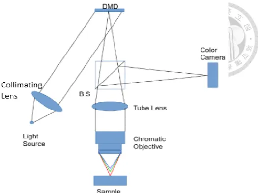
Figure 37 Digital diffractive-confocal imaging correlation chromatic microscope ... 49
Figure 38 Improve measurement range effect of chromatic objective ... 50
Figure 39. Bayer filter for color camera ... 50
Figure 40 Refraction occur between 2 isotropic media ... 51
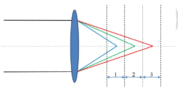
Figure 41 Axial chromatic dispersion: each wavelength is focused at a different point along the optical axis ... 52
Figure 42 Basic configuration of point-scan chromatic confocal microscope ... 53
Figure 43 Intensity curve registered by the spectrometer ... 54
Figure 44 Chromatic confocal calibration curve ... 55
Figure 45 Spectral Data Cube ... 56
Figure 46 Typical spectral imaging approaches. (a) Whiskbroom. (b) Pushbroom. (c) Staring. (d) Snapshot ... 56
Figure 47 Fabry Perot effect ... 57
Figure 48 Fabry Perot filters ... 58
Figure 49. IMEC Mosaic spectral area camera ... 58
Figure 50 Quasi one-shot full-field chromatic confocal microscope ... 60
Figure 51 Revised configuration for quasi one-shot full-field chromatic confocal microscope (illumination mode – configuration 1) ... 61
Figure 52 Revised configuration for quasi one-shot full-field chromatic confocal microscope (illumination mode – configuration 2) ... 61
Figure 53 Revised configuration for quasi one-shot full-field chromatic confocal microscope (illumination and detection mode) ... 62
Figure 54 Spectral response curve ... 63
Figure 55 Optical simulation of chromatic objective :(a) 20× chromatic ... 64
Figure 56 Optical simulation of the dispersion range with respect to various light wavelengths for the design of the chromatic objective: (a) 20× chromatic objective, (b) 27× chromatic objective... 65
Figure 57 IMEC camera spectrum response corresponding to one pinhole at different depths ... 66
Figure 58 3 layers of control software ... 67
Figure 59 Software interface for digital diffractive-confocal imaging correlation microscopy ... 68
Figure 60 Software interface for chromatic confocal microscopy using DMD and IMEC camera ... 69
Figure 61 Reducing database’s size ... 70
Figure 62 Timeline for parallel processing mode ... 70
Figure 63 Optical system setup on anti-vibration table ... 72
Figure 64 Alignment steps ... 73
Figure 65 Light collimating system ... 74
Figure 66 Placement of objective and tube lens ... 75
Figure 67 Flowchart for confocal effect checking ... 76
Figure 68 Intensity–depth response curve for 2x objective ... 76
Figure 69 Intensity–depth response curve for 20x objective ... 77
Figure 70 Flowchart of digital diffractive-confocal imaging correlation microscope .. 78
Figure 71 3-D images of wafer surface at different position ... 79
Figure 72 2-D and 3-D views of step-height sample ... 80
Figure 73 Defected sample. ... 80
Figure 74 3-D view of defected sample ... 80
Figure 75 Optical system setup on anti-vibration table for digital diffractive-confocal imaging correlation microscope goes chromatic ... 82
Figure 76 Flowchart of digital diffractive-confocal imaging correlation microscope goes chromatic ... 83
Figure 77 Typical NCC-depth response curve for digital diffractive-confocal imaging correlation microscope goes chromatic at position 1 – blue range ... 84
Figure 78 Typical NCC-depth response curve for digital diffractive-confocal imaging correlation goes chromatic at position 2 – green range ... 84
Figure 79 Typical NCC-depth response curve for digital diffractive-confocal imaging correlation microscope goes chromatic at position 3 – red range ... 85
Figure 80 2-D and 3-D views of step-height sample ... 85
Figure 81 Optical system setup on anti-vibration table for chromatic confocal system using DMD and IMEC camera ... 87
Figure 82 IMEC 16 bands snapshot mosaic filter layout ... 88
Figure 83 Filter responses in the active range of a SSM 4x4 VIS hyper spectral sensor 89 Figure 84 Spectrum response after calibration ... 90
Figure 85 Typical response of IMEC camera (16 bands) ... 91
Figure 86 Typical response of IMEC camera (single bands) ... 91
Figure 87 Flowchart of chromatic confocal system using DMD and IMEC camera ... 92
Figure 88 Auto-locate pinholes algorithm output ... 93
Figure 89 Typical NCC response ... 93
Figure 90 Scatter plot for accuracy and precision test ... 94
Figure 91 Diffuse surface sample ... 95
Figure 92 Typical NCC response ... 96
Figure 93 NCC response with noise ... 96
Figure 94 Scatter plot for accuracy and precision test of diffuse surface sample ... 97
Nomenclature
DMD Digital micro-mirror device N.C.C Normalized cross correlation SPM Scanning probe microscopy SEM Scanning electron microscopy NA Numerical aperture
PZT Piezo electric transducer FHWM Full width half maximum OPD Optical path difference
DDCICM Digital diffractive-confocal imaging correlation microscopy ( , )
S v w Light source distribution pattern function ( , )
P Pupil function ( , )
D v w Sensitivity function of detector ( , , )
I u v w Intensity function ( , , )
h u v w Fourier transform of the pupil distribution ( , , )
t u v w Projection pattern out-of-focus function
0( )
J x First-order Bessel function , ,
u v w Normalized optical coordinates ( , , )
W u v w
Wave front function including focusing and aberration terms
and Normalized pupil coordinates
It Total intensity in sub-image area
Wavelength
n Refractive index
Standard deviation
1 Introduction
1.1 Background
For past few decades, there are many advantaged new machines being developed by the commercial exploitation of micro- and nanotechnology (MNT). The rapid development of micro-nano system technology requires new devices, which has the ability to control and measure the product features as we move into a miniaturized world.
Nowadays, inspection is extremely important in the manufacturing process.
Inspection helps manufacturers control both catastrophic failure and defects, so they can increase the product’s quality and reduce wasted product. In micro-nano scale product, the surface features play an important role for characteristics and quality of a part.
Therefore, the key input information for micro-nano inspection processes usually is surface texture properties of micro-nano objects.
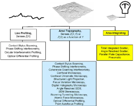
Surface profile measurement and areal surface texture measurement are both important input for micro-nano inspection processes. However, the measurement of areal surface texture has a number of benefits over profile measurement. There are currently many commercial instruments that can measure areal surface texture showed in Figure 1.
We can classify these devices by judging their surface texture measuring performance (line profiling, areal topography, or area-integrating) or measuring procedure (non- contact or contact type) in Figure 2.
Figure 1 Surface measurement devices
Surface texture measurement can be divided into two categories: contact type (SPM, Stylus) and non-contact type (SEM, optical). For industrial sample measurement, the optical type is usually a better approach because it does not require contacting with the sample and is easy to integrate with available product lines. In the 21st century, there are a lot of different optical instrument developed for surface texture and form measurement.
The interferometers with phase shifting technique could be accurately tracked for the peaks and valleys of the surface texture with nano-scale vertical resolution. The first of these was the phase shifting interferometry (PSI) microscope in the early 1980s, which was primarily useful for measurement of smooth optical surfaces. Flowing this invention, vertical scanning interferometer or scanning white light interferometer was developed in order to measure surfaces with higher roughness. Optical surface profilometry continues its success with confocal microscopes which were invented in the 1990s. Nowadays, these two types of instruments occupy big portion of the market for optical surface topography instruments.
Figure 2 Surface measurement devices measurement range
Optical confocal microscope has become extremely important for surface topography because of its high longitudinal measurability range and excellent vertical resolution. This kind of microscope is widely used to measure volume structures or surface topographies. Before, confocal microscopes was used mainly in the field of biology and medicine to visualize the three-dimensional structure of cells. Now, those systems were widely used in semiconductor industries for inspection purposes. There are many inspection systems using optical confocal microscope principle, which are widely used in manufacturing processing. Figure 3 shows some product from OLYMPUS, POLYTECH, KEYENCE, SENSOFAR and STIL.
(a) (b) (c)
(d) (e)
Figure 3 Commercial microscopes: (a) OLYMPUS Vertical scan laser confocal;
(b) POLYTECH Vertical scan laser confocal; (c) KEYENCE Vertical scan white light interferometry; (d) SENSOFAR Virtual confocal; (e) STIL Chromatic confocal
1.2 Statement of the problem
The goal of optical confocal surface profilometry is to measure volumetric structures or surface topographies with high accuracy and precision. This work is still a challenging task in this field because although traditional confocal microscope system help us to get higher accuracy and precision, it still requires scanning processes. Therefore, the time spent for measurement will be increased, and mechanical movement for scanning process can generate undesired errors in our measurement results.
Recent years, many different methods have been developed into confocal systems to improve the spatial resolution, the working distance, and scanning process. Most of the approaches try to maximize the simultaneous parallelization of confocal topography
measurements. Therefore, mechanical movement can be reduced or completely avoided, so the measuring times shortened. In general cases, to maintain the advantages of confocal microscope system, the approaches just can reduce the scanning process in 1 or 2 directions. However, almost the approaches still required complex setup, specific elements, troublesome calibration process and usually only applied for some specific samples. This makes these systems lack of flexibility.
Moreover, optical confocal surface profilometry is very time consuming in scanning process. To meet the requirements of industrial applications, the measuring time factor is the most important and, as such, it has the first priority to be improved.
Finally yet importantly, precedent confocal methods heavily relied on light intensity, the measured value can easily be effected by sample’s surface reflectance or light source’s power variation. Many confocal systems have been suffered from light intensity variation, so were hard to maintain with high precision and accuracy. Therefore, it is necessary to develop new methods, which can be immune to light intensity variation.
1.3 Research objectives
This research proposes an area-scan confocal surface profilometry system, which based on two new advanced devices: Digital Micro-mirror Devices (DMD) and IMEC spectral area-scan camera. In order to achieve maximum parallelization, we need to eliminate both lateral scanning and vertical scanning processes. By using DMD, lateral scanning will be reduced and mechanical movement in our system will be minimized, so measurement errors are also significantly reduced. Furthermore, with specific designed pinholes array arrangement being created by DMD, the cross-talk effect between adjacent measuring points can be significantly reduced, so lateral resolution could be also improved. In this study, the vertical scanning process will be eliminated by using two different approaches: innovative digital diffractive-confocal imaging correlation microscope and chromatic confocal system including spectral area camera.
In the first method, quasi one-shot full-field surface profilometry using digital diffractive-confocal imaging correlation microscope that is based on DMD is developed for quasi one-shot microscopic 3-D surface measurement. Optical configuration applied confocal microscope setup and was developed by using DMD to generate specific pinhole array arrangement for minimizing cross talk effect. The innovative method was developed to create normalized cross correlation – depth response curve from diffraction patterns of
pinhole. Using this approach, the sub-micrometer scale depth can be detected with high accuracy and precision.
In the second method, the spectral area camera will make are-scan chromatic confocal surface profilometry become robust and flexible. To apply these two devices to chromatic confocal system, we need to analyze the effect of virtual pinhole size, which is generated by the DMD light pattern, and the cross talk effect between adjacent virtual pinholes, then to develop an appropriate scanning strategy for the approach. On the other hand, spectral area camera have finite wavelength bands, so a new calibration process needs to be developed to increase the wavelength resolution. Moreover, a new method needs to be developed to establish the calibration curve based on the relationship between the scanning vertical distance and the spectral intensity.
1.4 Expected outcomes
In order to satisfy the high requirements in the modern industry about the speed, flexibility, precision, stability and reliability, this research will focus on developing area- scan confocal surface profilometry using DMD and spectral area camera, which satisfy the most important things as follows:
- Quasi one-shot full-field;
- Compact and lightweight;
- High accuracy and high precision with short measuring time;
- Robustness and efficiency.
2 Literature review
The confocal measurement principle makes use of a pinhole filter to filter the reflected stray light. When the sample is not in the focal position, the reflected light will not pass through the pinhole then to the light sensor; on the contrary, when the sample is on the focal position, reflected light will go through the pinhole to the light sensor, then gives a strong signal. This research focuses on maximizing parallelization of the developed confocal surface profilometry system, so literature review section will be divided into several subsections based on parallelization of each system. Literature review will come through from traditional confocal systems to chromatic confocal systems, from point scanning to area scanning confocal systems. All the systems in literature review section are grouped and listed in the table shown below:
Table 1 Classification of reviewed confocal system
direction scanning direction scanning direction scanning Zero direction scanning
Traditional confocal microscope
Confocal microscope using Nipkow disks
Noninterfero metric differential confocal microscope
3-D inspection using DMD
Time- resolved confocal
Polychromatic differential confocal microscope
Point-scan chromatic confocal microscope
Line-scan chromatic confocal microscope
Area-scan chromatic confocal microscope
microscopy using DMD
2.1 Traditional confocal microscope
Scanning confocal microscope is a well-established imaging tool, which has widely used for surface topography measurement because of its superior lateral and vertical resolution compared to conventional microscope [1]. It has played an important role in different fields, especially in in-situ automatic optical inspection (AOI) on microstructures [2]. Confocal microscopes are applied to surface profile detection for its high resolution, depth discrimination and unique sectioning capability; and, many efforts have been made to improve its property [3].
In a confocal microscope, a point light source illuminates the object through an objective, and the reflected light formed image on a point detector, which is employed to measure intensity of the reflected light. The point detector is achieved using a pinhole in front of the detector. A basic configuration of traditional confocal microscope is illustrated in Figure 4. Only the light that is reflected from the focal plane of the system, can pass through a pinhole, and then hit to the point detector. This create a strong optical sectioning property, which can be used to investigate the three-dimensional structure of thick objects. On the other hand, the pinhole also rejects light scattered from the optical system, so image clarity and measurement accuracy can be both improved [4].
Because the confocal microscopy only focuses on a single point in 3-D space, in order to build up a complete volumetric structure or surface topography of measuring sample, the system needs to perform both lateral scanning (X, Y direction) and vertical scanning (Z direction). Traditional confocal microscopes usually use a moving stage (servo motor stage or PZT) for scanning process. Based on the reflected light intensity signal, which will be maximum when the measuring sample is at the focal position, the volumetric structure of surface topography of measuring sample can be reconstructed.
Figure 4 Structure of traditional confocal microscope.
2.2 Confocal microscope with Nipkow disks system
A compact high-resolution scanning confocal microscope, using a micro lens and Nipkow disks has been developed by Takeo Tanami and other researchers to improve the scanning speed of confocal microscope system [5]. Figure 5 illustrates the construction of the microscope, which consists of two disks. The upper disk consists of micro lenses and the lower disk consists of pinholes. The pinholes and micro lenses are placed on two disks with the same special pattern. The collimated light from a laser illuminates on the upper disk, and then the light is focused onto the lower disk by the micro lenses. After that, the objective lens focuses the light onto a spot on the specimen. Going through the same path reflected, a beam splitter would reflect light from the specimen, and then forms an image on the camera through a relay lens. The two disks are connected together, so when they finish one rotation, the confocal microscope will finish the whole area of measuring specimen. This mechanism can increase the lateral scanning speed and can also speed up to 1 frame/ms with the Nipkow disk consists of ~20000 pairs of pinholes and micro lenses. The system has a high lateral scanning speed but reduces image quality (depending on the number of micro lenses and pinholes pairs). Moreover, the rotating movement of Nipkow disk may induce undesired mechanical vibration, which affects measurement quality.
Figure 5 Nipkow disk structure [5]
2.3 Noninterferometric differential confocal microscope
The concept of differential confocal microscope was proposed to utilize a linear variance ratio of intensity at the slopes of the axial response curve to measure surface contours with high axial resolution [6].
Figure 6 Noninterferometric differential confocal microscope’s structure [6]
Although when the sample is at the focal point, the light intensity is maximum. The derivative of the response curve with respect to the sample position becomes zero as in Figure 7. In order to increase the sensitivity to sample height variation, the sample needs to be placed slightly away from the focal point. From this setup, we can create differential response curve as in Figure 8.
Figure 7 Axial response curve of a confocal microscope [6]
Figure 8 Differential response of our differential confocal microscope with various objective lenses: (a) 60X, NA = 0.85; depth resolution = 2 nm; dynamic range = 0.7 pm.
(b) 40 X, NA = 0.65; depth resolution = 4 nm; dynamic range = 1.3 pm. (c) 20 X, NA = 0.40, depth resolution = 12 nm; dynamic range = 3.6 pm [6]
Even thought, the configuration made the system more insensitive to height variation, this system still needs to scan in X, Y and Z direction. There was no improvement in measurement parallelization.
2.4 Polychromatic differential confocal microscope
A differential confocal microscope based on polychromatic illumination was developed in order to gain both a wide measurement range and a high lateral resolution [7].
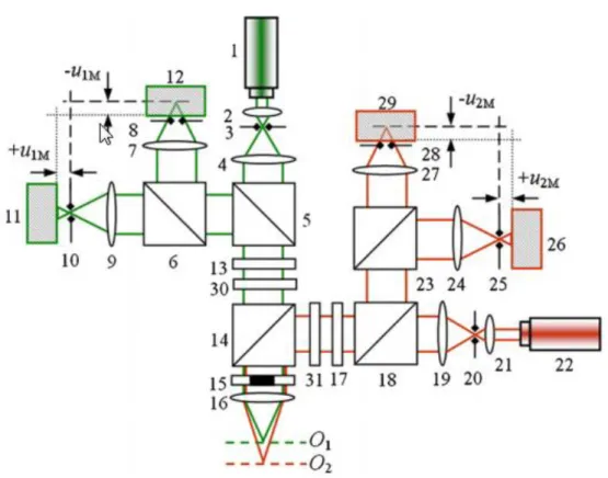
Figure 9 Schematic diagram of DCMBPI (lasers 1, 22; focusing lens 2, 21;
pinholes 3, 8, 10, 20, 25, 28; extender lens 4, 19; polarized beam splitters 5, 18; beam splitters 6, 23; λ / 4 wave plates 13, 17; depolarized beam splitter 14; collecting objectives 7, 9, 24, 27; center shaded filter 15; objective 16; detectors 11, 12, 26, 29;
monochromatic filters 30, 31; focal planes O 1 , O 2 ) [7]
The idea for this system based on the fact that axial response can be shifted with its curve when a detector is shifted from its imaging focal plane. That means that setting the detectors being defocused from their imaging focal planes will shift the axial response curves being shifted either forward or backward [8]. Figure 9 shows the configuration of
polychromatic differential confocal system. In this system these detector 11, 12 29 and 26 are shifted away from focal point, in order to generate differential signals. By using two light sources with different wavelength, this system can increase the measurement range. The differential signals are calculated by using the formula:
With the differential signals detected, we can inverse one of those signal and combine it together to form a lager measurement range.
Figure 10 Extended response range based on polychromatic illumination. (a) Response of the differential detector group. (b) Synthetic uniform response range of
DCMBPI [7]
By introducing polychromatic illumination, two independent ranges can be stitched together to form an extended measurement range. The system already eliminates vertical scanning but still requires lateral scanning. However, in this method, there still exist some drawbacks, which may affect the accuracy and its potential application. The system based on two light sources with four light detectors can make its structure more complex and hard to calibrate. Limited by the number of light sources, the measuring range cannot be extended further.
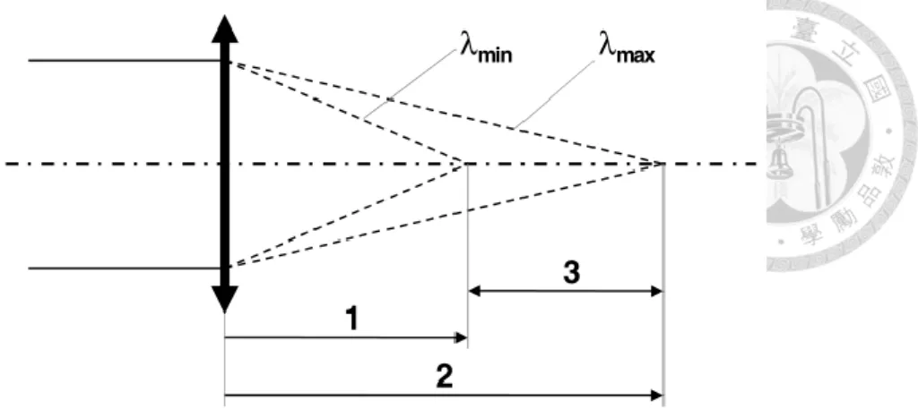
2.5 Point-scan chromatic confocal microscope
Chromatic confocal technique with an exemption for vertical scanning and can achieve real-time measurements [9, 10], and the advantage of long depth measurement
range [11]. The chromatic confocal point sensor achieves a complete parallelization of the depth scan.
Applying chromatic effects of the imaging lens is a possibility to eliminate the vertical scanning process. The intensity curve from traditional confocal microscope now transform to spectrum curve as described in Figure 11. After mapping the wavelength and the distance of focal plane for each wavelength, we can get the height of measuring sample from spectral intensity.
Figure 11 Confocal intensity signal a) with mechanical depth scanning and b) with chromatic depth scanning [9]
In a point scan, chromatic confocal setup can use a varying illumination wavelength or use a spectrally broad light source and a spectrometer as a detector. Figure 12 illustrates the second configuration.
Figure 12 Structure of point-scan chromatic confocal microscope [9]
2.6 Line-scan chromatic confocal microscope
Chromatic confocal point sensors does not need vertical scanning but it is still necessary to perform spatial scanning to reconstruct a surface topography. A further parallelization can be achieved by using chromatic confocal line sensors.
By applying cylinder lens and using a slit aperture instead of a pinhole, this system can reduce lateral scanning in one direction. In this system, the line-spectrometer can be employed to maintain lateral resolution.
Figure 13 Chromatic confocal line sensor [9]
The line-scan chromatic confocal microscope can eliminate the depth scanning and reduce the lateral scanning in one direction. However, this system may suffer from cross- talk effect between adjacent points in scanning line.
In the developed system, the optical system was designed for a relatively high NA of 0.4 for a field diameter of 2.4 mm. The achieved chromatic depth measurement range was 0.7 mm. A slit aperture just can eliminate cross talk effect in one direction. Therefore, its depth discrimination property is poorer than that of a pinhole. The confocal depth is plotted in Figure 14 and it has a FWHM of 55 µm.
Figure 14 Confocal depth response [9]
2.7 3-D micro-inspection goes DMD
Digital Micro-mirror Devices (DMD) was employed for applications in the field of optical metrology are also possible. Modern DMDs consist of many micro-mirrors made of an aluminum alloy. The single micro-mirrors can be control to switch a tilting angle.
Usually, a single micro mirror has 3 states: ON, OFF, and REST respectively to 3 different tilting angles.
Figure 15 Image of a complete DMD [12]
F. Bitte and his partners already developed 3-D inspection system using the new devices [12] .In this configuration, the DMD is used to project an array of small spots resulting either from single mirror elements (pixels) or composed multiple mirror
elements (super pixels). These spots act as multiple point light source. The light from those spots are imaged onto the specimen surface by a microscope objective, then is reflected back and forms images onto the camera chip where their intensities are measured by specific camera pixels.
DMD
Specimen Light
source Collimator
Achromatic lenses
CCD Beam
splitter
Microscope objective
Z
Figure 16 Schematic illustration of the DMD based optical surface profiler [13]
The pixel-intensities are maximum when the corresponding images, which created by DMD pixels are lying in the focal plane of the microscope objective. By doing vertical scanning, the intensity-depth response curves for every measurement point can be recorded. After detecting intensity peak in each intensity–depth response curves and link it to corresponding motor position, the 3-D profile of the specimen can be reconstructed.
In this system, by applying DMD for lateral scanning, the speed is significantly increased. However, this system still requires vertical scanning and lacking of pinhole.
This may lead to reduce measurement accuracy and precision. Although special lateral scanning strategy was already developed, without using a real pinhole, the system may still suffer from the cross-talk effect between adjacent imaging points.
2.8 Time-resolved confocal microscopy using DMD
Time resolved 3-D-microscopy using DMD-arrays is a flexible confocal system.
The system is optimized for optical imaging of reflective, transparent, and fluorescent objects [14. The configuration of this system is illustrated in Figure 17.
Figure 17 Optical layout of a DMD-confocal microscopy system [14]
The working principle of this system is almost the same with 3-D-inspection using DMD. However, in this application, DMD realizes both the illumination and the confocal sectioning through a DMD-array. Just by changing the order of beam splitter and DMD, the DMD now has a role acting like a virtual pinhole in front of the light source and in front of CCD. This configuration will improve the sectioning capability and reduce cross- talk effect between adjacent scanning points.
In this system, the DMD-array consists of a rectangular grid, in this case of 1024x768 square micro-mirrors. Each mirror measures 12.6 μm to a side, with a distance of 1 μm between mirrors, the overall dimensions of the array are approx. 14x10 mm. Each micro-mirror can be set into one of three states: on, off, and resting. The switch rate can be up to 8 kHz. Based on this device, the system can flexibly changes between different illumination modes such as point-scan, multiple point-scan, line-scan and multiple line- scan.
(a) (b) (c) (d)
Figure 18 Examples of employed DMD scan patterns: a) point scan, b) line scan, c) multi-line scan, d) multipoint scan [14]
Figure 18 shows the axial resolution of the DMD confocal scanning microscope for different scan pattern configurations (1x1, 2x2, and 4x4 mirrors).
Figure 19 Plot of the axial resolution of the DMD confocal scanning microscope [14]
Like 3-D-inspection using DMD system, by applying DMD for lateral scanning, the scanning time of this system is reduced. On the other hand, because of no mechanical movement, the error due to mechanical vibration is eliminated. Furthermore, changing the order of DMD and beam splitter has solved the lacking-pinhole problem, leading to improvement of measuring result’s quality. However, this system still requires vertical scanning.
3 Research methodology
In order to archive quasi one-shot full-field confocal surface profilometry, in both developed methods (digital diffractive-confocal imaging correlation method and chromatic confocal system including spectral area camera), our systems relies on confocal microscope theory, specific designed pinholes array created by Digital Micro-mirrors Devices (DMD) and spectral area camera. Before illustrating how these two approaches can be suitable for quasi one-shot full-field confocal profilometry, background knowledge and working principle of confocal and chromatic confocal microscope system will be first introduced, and then followed by the overview of DMD.
3.1 Confocal microscope
A confocal microscope will take a series of images of object when doing vertical scanning through the depth of focus of the objective. By the way, it can detect the image with the highest intensity and calculate the height or depth of measuring object. Confocal microscopy has many advantages over other optical measuring techniques such as having a high numerical aperture that can bring in high measureable local slope with high light intensity efficiency or high lateral and vertical resolution. In the beginning, confocal microscopy was mainly used in biomedical field, however, the application field of the device quickly become very broad, ranging from biomedical to semiconductor, optics, and more.
3.1.1 Basic structure and working principle of confocal microscope
Basic configuration of confocal microscopy is described in Figure 20. In such a configuration, a pinhole is located right in front of laser point source (an illumination pinhole). The light goes through the illumination pinhole to a beam splitter and projects on the sample by an objective lens. The smallest illuminated spot is achieved on the focal plane of the objective and is typically a diffraction-limited spot. When the light hits the sample surface, it then reflects back and goes through the detection pinhole (confocal aperture) to the detector. The illumination pinhole and detection pinhole mutually have a conjugate optical relation.
Figure 20 Point-scan confocal microscope (object at focal plane)
When the measured object’s surface is placed exactly on the focal plane of the objective, the reflected light will have a maximum intensity. On the other hand, when the measured object’s surface is not on focal plane, the reflected light defocuses away from detection pinhole (Figure 21). All the stray lights will be blocked by the detection pinhole, so the intensity of this measuring point on the detector will be significantly reduced.
Figure 21 Point-scan confocal microscope (object out of focus)
Based on the characteristics of the confocal microscope, we can detect the height or the depth of measurement point on surface’s sample. Vertical scanning procedure can be performed using a PZT or servo stage in order to generate intensity respond curves corresponding to individual points on the measured object’s surface shown in Figure 22.
Using peak detection algorithm and stage’s depth location, we can calculate the height or depth of those points. To generate surface profile or surface 3-D topography, we can use mechanical (PZT or servo stages) or optical (Nipkow Disk or DMD) devices for lateral scanning to scan a line or an area on the object’s surface.
Figure 22 Intensity respond curve
3.1.2 Confocal microscope image formation
A schematic diagram of a typical scanning optical microscope is shown in Figure 23.
Figure 23 Point-scan confocal microscope modeling
A light source pattern of distribution ( , )S v w illuminates a microscope’s objective with a pupil functionP( , ) . The light is focused onto the sample with reflectance distribution r and is reflected back to the objective with the same pupil function and then focused onto a detector with sensitivityD v w( , ) . The intensity on a single point of the detector with incoherent propagation is given by
( , , ) ( , ) ( , ', ') h(0, ', ')2 ' ' I u v w D v w t u v w v v w w dv dw
(1) where ( , ', ')t u v w is the projection pattern out-of-focus by a quantityu , diffraction limited on the object plane, / 2u being the distance between the surface and the object plane, given by
( , ', w') ( '', '') ( , ' '', ' '')2 '' ''
t u v S v w h u v v w w dv dw
(2) where ( , , )h u v w is the Fourier transform of the pupil distribution
( ) ( , , )
( , , ) ( , ) i v w i W u v w h u v w P e e d d
(3) The terms v and w are the normalized optical coordinates
2 sin 2 y sin
v x
w
(4) And sinα is the numerical aperture of the objective, and are the pupil coordinates normalized to the aperture radius of the pupil, x
a, y
a, and W u v w( , , ) is the wave front including focusing and aberration terms.
Equation (2) can be expressed as a convolution by
( , , ) ( , ) | h( , , ) |2
t u v w S v w u v w
(5) Resulting in a simplified expression for equation (1) as
2 2
( , , ) ( ( , ) | h( , , ) | )( ( , ) | h(0, , ) | ) I u v w S v w u v w D v w v w
(6) On a circular pupil, such as those present on a typical microscope objective
sin
(7) And Equation (3) is simplified to
1
( , ) 0
0
( , ) ( ) ( ) i W u
h u v
P J v e d(8)
where J x is a first-order Bessel function of the first type. The defocus term for 0( ) the wave front in the pupil region is expressed as
1 2
( , )
W u 2u
(9) where
8 2
sin ( / 2)
u z
(10) Equation (8) is simplified to
1 1 2
2 0
0
( , ) ( ) ( ) i u
h u v
P J v e d(11)
3.2 Digital micro-mirrors devices (DMD)
Modern DMD consists of many micro-mirrors made of an aluminum alloy. The single micro-mirror is both an opto-mechanical element and an electro-mechanical element, which can be controlled to switch tilting angle.
Figure 24. Pixels in On and Off state
The DMD pixel is an electro-mechanical element in that there are three stable micro-mirror states corresponding to different tilting angles. By programing the DMD controller, individual micro-mirror can be set into one of three working states (on, off and resting). In our systems, the DMD acts as a spatial light modulator as well as a pinhole array creator. By convention, the positive (+) state is tilted toward the illumination and is referred to as the "on" state. Similarly, the negative (–) state is tilted away from the illumination and is referred to as the "off" state.
Figure 25 Pixel with Labeled Parts
Mechanical structure of a DMD pixel was illustrated in Figure 25. The diagram shows a micro-mirror in the unpowered state. The two electrodes shown are used in holding the micro-mirror in on or off positions (+12° and -12°).
Based on the characteristics of the device, it can be used to control illumination light and reflect light in confocal system. DMD not only reduces the measuring time and mechanical vibration error, but also makes the system more flexible because the system can switch among scanning mechanisms (point-scan, line-scan, area-scan) just by changing scanning pattern in software.
In our application, we use DMD from Texas Instrument. In order to get the highest on-off frequency, we use DMD with diamond arrangement micro-mirrors as described in Figure 26. Figure 27 shows the specific alignment to make incident light and reflected lights follow designed paths. Because of diamond arrangement, to setup our system on
anti-vibration table, which requires incident light and reflected lights to be co-planar, we need to rotate DMD 45 degree.
Figure 26 DMD orthogonal and diamond arrangements
Figure 27 DMD incident light and reflected light configuration
3.3 Digital diffractive-confocal imaging correlation microscope based on DMD
In order to speed up the measuring speed of confocal system but to remain high sectioning capability and spatial resolution, our idea is to use the diffraction pattern of virtual pinholes, which are created by micro-mirror on DMD to encode depth information.
Then, using the reverse procedure to decode the depth information from pinhole's diffraction patterns to depth. Applying this principle will strengthen measurement efficiency by many factors. First, by building diffraction database and extract the depth information from this database, the vertical scanning process can be totally omitted. On the other hand, based on DMD, there are a large number of pinholes matrix can be created, so in in-situ application, spatial scanning processes can be skipped. For applications which require higher spatial resolution, spatial scanning processes can be performed using different specific pinhole matrix arrangement which created by DMD. In this method, there are no requirements for both axial and lateral scanning; therefore, the developed system can improve in both measurement speed and quality. Before, to omit one scanning direction in confocal microscope, we always need to stick with complex setup of differential confocal microscope or specific spectrometer in chromatic confocal microscope. In our method, we just based on simple optical configuration with a 12-bit mono CCD. With this approach, confocal microscope system can be optimistic for in-situ surface measurement because of quasi one-shot full-field capability.
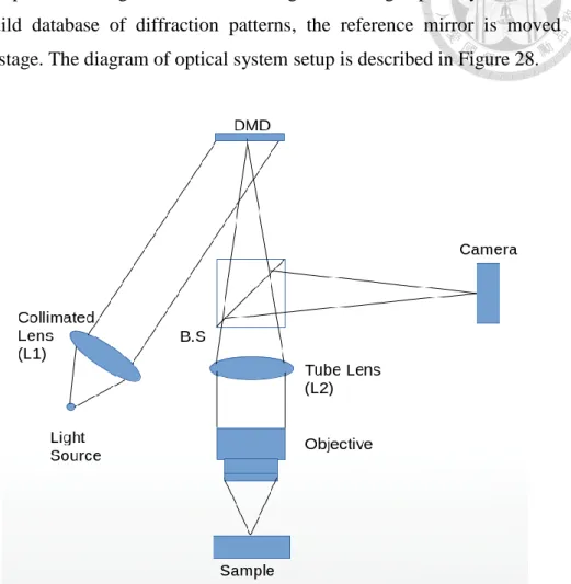
To achieve the above-mentioned approach, this article proposes one novel optical configuration of confocal microscopy using DMD. The configuration uses digital micro- mirror device (DMD; Texas Instruments, Dallas, Tex.) as spatial light modulator in confocal microscope configuration with white-light light source. A white-light light source beam is collimated by lens L1 to illuminate the DMD. The reflected light from DMD is collimated again using tube lens L2 and imaged on the object plane of the objective. The mirror (or test sample) is placed perpendicular to optical axial of objective, so reflected light from the mirror go through objective again and is imaged on to high speed 12-bit CCD camera by tube lens L2 and beam splitter BS. In order to make optical configuration simple and flexible as much as possible, the configuration employed illumination only mode of Programmable Array Scanning Confocal Microscope configuration, where the pixels of DMD are used to restrict the light projected onto the surface while the optical sectioning is achieved by the use of the pixels of a CCD camera.
Each element of the micro-display corresponds to pixels on CCD camera. None the light from out-of-focus regions falls on neighboring pixels is taken into account. The system applies virtual pinhole configuration to remain high sectioning capability with a robust setup. To build database of diffraction patterns, the reference mirror is moved by piezoelectric stage. The diagram of optical system setup is described in Figure 28.
Figure 28 Diagram of optical system setup for digital diffractive-confocal imaging correlation microscope.
3.3.1 Pinhole’s diffraction pattern
In digital diffractive-confocal imaging correlation microscope, those micro-mirrors of the DMD are used as square micro-pinholes and as square aperture, which can create diffraction patterns needed for encoding and decoding depth information. In this configuration, the light from point light source is collimated by lens L1, and then hit to DMD. Those micro-mirrors of the DMD act as square aperture, distance from DMD to sample are rather large compared to the size of square aperture, so the diffraction patterns created by DMD micro-mirrors need to follow Fraunhofer diffraction theory.
To understand the principle of calculation of the Fraunhofer diffraction from a simple rectangular aperture, let us consider Figure 29.
Figure 29 Fraunhofer diffraction from a rectangular aperture
The Fraunhofer diffraction of a plane wave incident normally on such a rectangular aperture will be given by
/2 /2
2 2
/2 /2
( , , ) exp ( )
2
b a
ikz iu iv
b a
A ik
u x y z e x y e d e d
i z z
(12) where we have chosen the origin to be at the center of the rectangular aperture (see Figure 29). Carrying out the integration, we obtain
2 2 sin sin
( , , ) exp ( )
2 A ikz ik
u x y z e x y
i z z
(13) where is given by
sin 2
ub bx b
z
(14) and is given by
sin 2
va ay a
z
(15) where represents the angle of diffraction along the y direction.
Thus, we may write for the intensity distribution
2 2 0
sin sin ( )
I P I
(16) The diffraction pattern for square pinhole is illustrated by Figure 30 and Figure 31.
Figure 30 2-D and 3-D visualization for Fraunhofer pattern of a square aperture (computer generated)
Figure 31 2-D and 3-D visualization of the same pattern but with increased exposure time to bring out some of the faint terms (computer generated)
For far field diffraction, when the distance between aperture and screen is increased, the diffraction pattern will become larger and less contrasted but it tends to keep the same pattern. However, by applying confocal microscope setup, with in- and out-focus effect the diffraction pattern we see on camera will change when the distance between sample and objective is increased or decreased. Therefore, with each depth position, we will have the corresponding imaged diffraction pattern. This will be signature pattern for this depth and can be used for depth encoding and decoding process.
In our application, because of light intensity, these pinholes created from DMD micro-mirrors consist of four micro-mirrors arranged in symmetric configuration as
showed in Figure 32. The diffraction pattern generated by this configuration is different from a simple single rectangular aperture. The diffraction pattern will be superposition of four Fraunhofer diffraction patterns from four square micro-mirrors.
Figure 32 Pinhole’s configuration
3.3.2 Confocal effect
In the traditional confocal principle, pinholes are used to eliminate stray light get into optical system, also to prevent cross-talk effect between adjacent measuring points and between adjacent detecting sensors. When the object locates on the focal plane of a confocal layout, the reflected light from the object’s surface can pass through a pinhole and reach to the detector with a maximum light intensity. For the traditional confocal microscope, a vertical scanning process is required to generate a depth response curve of the light intensity. The light intensity being detected in the above conjugative optical configuration can be represented by Eq. (17).
sin( / 2) 2
( ) ( / 2) I u u
u
(17) where
2 0
8 z sin ( )
u 2
where is the wave - length of the light source; z is the vertical distance; and sin0 is the numerical aperture.
In the developed system, these pinholes created by controlling micro-mirrors on DMD are used to form one-to-one conjugate relation between each incident light and its corresponding detecting pixels. The conjugate relation will help to avoid the cross-talk problem in the full-field measurement. The DMD will be loaded with a specific pinhole array pattern, which is designed to spatially filter unfocused light and other possible stray lights away from the corresponding detecting sensor, thereby minimizing the lateral cross-talk between the detected image sensors.
When one lens is used for both objective and imaging lens, the light intensity function of acquired signals can be described as follows.
2
1 4
( /2)
0 0
( , ) 2 ( ) ju ( )
I u v
P e J v d(18) where P( ) denotes the pupil function of objective; J0
is the zero-order Bessel function, u and v are the normalized optical radii.
2 0
0
2 8
sin z sin ( )
v r u 2
(19) Furthermore, this configuration will cause the change of diffraction pattern when the incident light goes through the objective, hits with measuring sample's surface or reference mirror's surface, then reflects back and finally is imaged on the camera's sensor.
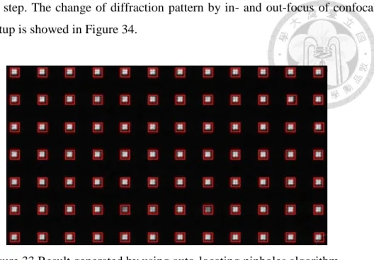
Based on this principle, we can replace the intensity-depth response curve by using normalized cross correlation-depth response curve and achieve a quasi one-shot full-field confocal microscope system. First, the specific pinhole array will be loaded into DMD, and then a reference mirror used to build a reference database. Vertical scanning calibration procedure was performed by using PZT. At each step – each vertical position, the 12-bit mono camera will take one corresponding picture. When measuring a sample, we just need to take one picture, and with the help of multiple pinholes array configuration generated by controlling DMD, we can achieve full-field measurement with one picture imaging. With the reference database being established, we can do special searching algorithm to find the best focus imaged position, size and location of each pinhole on the database images. The sample result of this step is showed in Figure 33. Because of in- and out-focus effect of the confocal configuration, each diffraction pattern of each pinhole is unique for each step height and can be used as a signature identifier for this
corresponding step. The change of diffraction pattern by in- and out-focus of confocal microscope setup is showed in Figure 34.
Figure 33 Result generated by using auto-locating pinholes algorithm.
Figure 34 Diffraction pattern change by in- and out-focus effect of confocal configuration.
With this process, each pinhole will have an array of sub-image being contained with diffraction patterns corresponding with step heights.
When measuring a sample, the camera just needs to take only one shot and based on pinhole's locations which can get from the last step, the sub-image contain diffraction patterns of those pinholes can be extracted. The extracted sub-images can be used to calculate the normalized cross correlation value based on the reference sub-images array of each pinhole by the Eq. (20).
,
2 2
, ,
( ( , ) ( , )) . .
( , ) ( , )
x y
x y x y
I x y R x y N C C
I x y R x y
(20) Therefore, each pinhole as well as each measurement point will have its own normalized cross correlation–depth response curve, illustrated in Figure 35. When the normalized cross correlation factor reaches to peak, this means the diffraction pattern of measuring point is identical with the diffraction pattern of reference point at this specific step. From that, we can convert the normalized cross correlation factor to depth information.
For the previous confocal microscope, an important factor affecting mesurement results is light intensity variation caused by undesired light source’s power fluctuating and reflectivity variation of sample’s surface. In our system, those disturbances can occur in both reference database image and measured image. In here, we assume that our light spot is small enough, so in this area, the sample’s surface has uniform reflectivity.
Therefore, those two disturbances can be modelled as one multiplicative mode disturbance n in Eq. (21); n is disturbance in measured image and I n is disturbance in R references database image. Eq. (21) will make our system immune to light intensity and surface reflectivity variations. This method can be practical to the object surface having a different absorb rate of optics from point to point.
,
2 2
, ,
,
2 2
, ,
,
2 2
, ,
( ( , ) ( , ))
. .
( , ) ( , )
( ( , ) ( , ))
( , ) ( , )
( ( , ) ( , ))
( , ) ( , )
I R
x y
I R
x y x y
I R
x y
I R
x y x y
x y
x y x y
n I x y n R x y N C C
n I x y n R x y
n n I x y R x y
n n I x y R x y
I x y R x y I x y R x y
(21) where x, y are coordinate of pixels, I is intensity one measured image and Ris the intensity in diffraction pattern database images.
![Figure 11 Confocal intensity signal a) with mechanical depth scanning and b) with chromatic depth scanning [9]](https://thumb-ap.123doks.com/thumbv2/9libinfo/9604649.630803/27.892.273.738.71.1043/figure-confocal-intensity-signal-mechanical-scanning-chromatic-scanning.webp)
![Figure 15 Image of a complete DMD [12]](https://thumb-ap.123doks.com/thumbv2/9libinfo/9604649.630803/29.892.195.769.725.962/figure-image-complete-dmd.webp)
![Figure 19 Plot of the axial resolution of the DMD confocal scanning microscope [14]](https://thumb-ap.123doks.com/thumbv2/9libinfo/9604649.630803/32.892.291.786.116.467/figure-plot-axial-resolution-dmd-confocal-scanning-microscope.webp)