目錄
中文摘要 2
英文摘要 2
1. 前言 --- 3
2. 研究目的 --- 3
3. 文獻探討 --- 3
4. 研究方法 --- 5
5. 結果與討論 --- 6
6. 結論與建議 --- 13
7. 計畫產出 --- 13
參考文獻 --- 14
附件 1. SCI 論文-1 --- 16
附件 2. SCI 論文-2 --- 20
附件 3. 國際學術會議論文 --- 25
附件 4. 韓國專利證書 --- 29
附錄二. 國科會補助專題研究計畫成果報告自評表
附錄三. 國科會補助計畫衍生研發成果推廣資料表
摘要
本計畫研究兩種電阻材質之電阻式記憶體,一種為摻銅二氧化矽,另一種為氧化鋯-氧化鎳複合薄 膜。於摻銅二氧化矽部分本研究成功的以共濺鍍技術製做電阻模層,並且在不需要預先以高電壓或高 溫活化的狀況下,即可以進行雙極式電阻切換。另一方面,本研究也成功的將昂貴的鉑下電極置換成 鋁、氮化鉭,使摻銅二氧化矽之電阻式記憶體可以進行可逆式電阻切換。最後本研究也將上電極由銅 置換為氮化鉭以成為氮化鉭/摻銅二氧化矽/氮化鉭結構,得到可靠度高的電阻式記憶體。
本研究於氧化鋯-氧化鎳複合薄膜的部分使用鋁材質取代鉑材質為上下電極,鋁/氧化鋯/鋁結構以 及鋁/氧化鋯-氧化鎳/鋁結構皆可進行單極式電阻切換。本研究發現純氧化鋯的缺氧程度影響電阻切換 性質,低缺氧程度之氧化鋯的高低電阻比值可高達 105,高缺氧程度之氧化鋯的高低電阻比值降到 103 以下。加入氧化鎳的氧化鋯之高低電阻比界於 102與 105之間,但是可以改善電阻切換時之電壓範圍重 疊問題。
本研究發表的研究成果如下:
(1) SCI 期刊已刊登一篇,審查中二篇,撰寫中一篇。
(2) 國際學術會議論文已發表二篇。
(3) 已獲得韓國專利一篇,同篇專利此時正於美國、日本、本國審查中。
關鍵字:電阻式記憶體、摻銅二氧化矽、氧化鋯、氧化鎳、濺鍍
Abstract
Two types of oxides were employed as resistive layer for resistive memory (RRAM). One was copper-doped silica (Cu-SiO2), the other was composites of zirconia and nickel oxide (ZrO2-NiO). For the study of Cu-SiO2 based RRAM, the resistive layers were prepared by sputter-deposition technique, and the resultant RRAM could be readily switched without need of prior forming procedure either by high voltage stressing or high temperature annealing. On the other hand, the uses of Al and TaN as the bottom electrode were developed, in replacement of precious Pt for the Cu-SiO2 based RRAM. Finally, the active Cu
electrode was replaced by an inactive TaN, and resultant TaN/Cu-SiO2/TaN RRAM exhibited reversible switching of resistance with good reliability.
The second part of this project studied ZrO2-NiO based RRAM using Al as both the top and the bottom electrode, in replacement of precious Pt. The Al/ZrO2/Al and Al/ZrO2-NiO/Al cells showed unipolar switch of resistance. Oxygen deficiency in the ZrO2 films influenced resistive switching properties. The ZrOx
RRAM with low oxygen deficiency had a resistance ratio of high resistance state (HRS) to low resistance state (LRS) as high as 105. The resistance ratio dropped to 103 for the RRAM of ZrOx with high oxygen deficiency. Resistance ratios were between 102 to 105 for the RRAM of ZrO2-NiO. Hence, the issue of overlapped ranges of SET and RESET voltages was resolved by adding NiO into the ZrO2 film.
Keywords: resistive memory, copper-doped silica, zirconia, nickel oxide, sputter deposition
1. 前言
人類文明已經隨著資訊科技發展躍昇,其中微電子元件之功能與積集密度隨時間呈指數成長為關 鍵推動力。積體電路發展歷程中已經發現元件尺寸逐步縮小的規律依循莫爾定律,數年之後積體電路 設計線寬將縮小至 15 nm 以下,部分元件在線寬縮小時無法展現應具備的功能,因此需要開發新的元 件技術與材料。技術。攜帶式存取裝置的主體為非揮發性記憶體,除了應用於電腦資訊儲存之外,也 可以應用於數位相機、手機等產品。目前非揮發性記憶體的設計以快閃記憶體為核心技術,但在未來 需要新的技術以便符合更小限寬與更高密度的要求,於正開發中的新穎非揮發性記憶體技術中的電阻 式記憶體(Resistive memory; RRAM)具有結構簡單以及易於積集化的特性,具有潛力在未來取代目前的 快閃記憶體。
2. 研究目的
電阻式記憶體具有潛力取代快閃記憶體成為新世代非揮發性記憶體,因此近年來逐漸受到重視 [1]。先前本實驗室於研究摻銅二氧化矽薄膜即觀察到其由絕緣體轉換成導體的特性[2,3],本研究進一 步研究其高電阻/低電阻循環切換特性,用以評估以摻銅二氧化矽薄膜為基礎的電阻式記憶體的實用 性,同時研究搭配合適且具經濟性的電極材質。先前本實驗室也研究過混合氧化鎳與氧化鋯之薄膜材 料[4,5],而由文獻報導得知單獨氧化鎳與氧化鋯皆具有電阻切換特性,因此本研究也選擇混合氧化鎳 與氧化鋯的薄膜為電阻式記憶體的電阻層,比較其與單獨氧化鋯之電阻式記憶體的操作特性。本研究 同時也以具經濟性的鋁為電極材質,取代穩定度高但是較昂貴的鉑電極,使本研究成果可以實用於新 世代積體電路。
3. 文獻探討
電阻式記憶體的單一記憶胞為由電阻層與上下電極組合之三層結構的元件(Fig. 1(a)),並可以以電 壓控制使其具有高電阻狀態(High resistance state; HRS)與低電阻狀態(Low resistance state; LRS),對應數 位儲存的 0 與 1,當以陣列式佈局於積體電路中(Fig. 1(b)),具有潛力成為未來的高儲存密度非揮發性 記憶體[1,6]。時
(a) (b)
Fig.1 (a) 電阻式記憶體單一記憶胞之 MIM 結構,以及(b)以絕緣材料與交叉之字元線及位元線電極組成的陣列式電阻 式記憶體示意圖[6]
電阻式記憶體使用電壓驅動方式令記憶胞於 HRS 與 LRS 狀態間切換,一具操作切換電壓之極性區分 為單極式切換(Unipolar switch)與雙極式切換(Bipolar switch)兩種形式[1,6]。單極式切換的電流‒ 電壓曲
線(I-V curve)如 Fig. 2(a),記憶體在 HRS 狀態時施加正偏壓至一個 SET 電壓值時會瞬間轉變成為 LRS,
此時記憶體為 ON,再次施加正偏壓時電流大增,一直到達一個 RESET 電壓時又轉變成 HRS,此時記 憶體為 OFF,而此種轉變為可逆式且可以循環操作;單極式記憶體的電阻切換也可以於負偏壓區域操 作,或是在相反極性偏壓操作,因此有時也稱為非極性切換(Nonpolar)[6]。雙極式切換的電流-電壓曲 線如 Fig. 2(b),記憶體若在 HRS 狀態時施加正偏壓至一個 SET 電壓時會轉變成為 LRS,但是需要施加 逆向的負偏壓才能轉變回 HRS [6]。
(a) (b)
Fig. 2. 電阻式記憶體的(a)單極式切換,以及(b)雙極式電阻切換的 I-V 特性曲線[6]
電阻式記憶體的 HRS 與 LRS 狀態轉換的反應機構有數種,本計畫研究的兩類材質形成 LRS 狀態 的機構屬於導電燈絲機構(Conductive filaments),如 Fig. 3 所示,於原本均勻的電阻薄膜內形成燈絲狀 的導電路徑,並且當電阻切換進行時於局部區域的導電燈絲遂行斷裂與連接交替行為 [6]。
Fig. 3. 導電燈絲於電阻式記憶體中相連接與斷裂行為示意圖[6]
本計畫研究的電阻式記憶體的第一種電阻層材料為摻銅二氧化矽(Cu-SiO2),屬於電化學電阻式記 憶體(Electrocemical RRAM),於 LRS 時會形成貫穿電阻層的銅導電燈絲[7]。文獻中這類電阻式記憶體 的結構一般包含一層銅電極與一層鉑電極,中間夾一層不含銅的氧化物,例如 Cu/SiO2/Pt [7-9]、
Cu/MoOx/Pt [10]、Cu/WOx/W [11]。由於電化學電阻式記憶體需要使銅、金或銀於電阻層內形成導電燈 絲,因此需要先以較高電壓或高溫使電極之金屬經由離子狀態進入絕緣膜中,進而形成導電燈絲之後 方可以進行電阻切換操作[8,12];部分研究則將電阻膜做成多層膜,並把金屬夾在其中一層或多層以便 利生成導電燈絲[9,13]。此類電阻式記憶體一般以雙極式操作電阻切換,導電燈絲於局部區域進行氧化 還原時銅分別以原子狀態(Cu0)聚集形成連續燈絲,或是變成氧化狀態(Cu+, Cu2+)遷移而使燈絲斷開。
本計畫於摻銅二氧化矽為電阻層的電阻式記憶體研究之重點有三項:其一為於製備電阻膜層時即將銅 摻入氧化物中,以利免除高電壓或是高溫驅入程序;其二為以比較經濟性的材料為下電極,取代昂貴 的鉑金屬電極;最後為避免過多銅成分被驅入電阻膜層中而造成永久短路,將銅上電極置換為其他材 質電極用以改善電阻式記憶體穩定性。
本計畫研究的電阻式記憶體的第二種電阻層材料為氧化鎳-氧化鋯(NiO-ZrO2)複合物,此構想一部
分源自先前研究的燃料電池電極材料中氧化鎳與氧化鋯不互溶特性[4,5],一部分源自文獻中的氧化鎳 電阻式記憶體與氧化鋯電阻式記憶體的研究。Gibbsons 與 Beadle[14]在 1964 年即發現氧化鎳可以具有 高電阻/低電阻切換特性,其原因與母相中形成燈絲狀鎳金屬相有關。氧化鎳電阻切換現象陸續被報導 相,其中鎳燈絲微觀結構與形成動力學至為重要,例如 Park 等人觀察到鎳燈絲延著氧化鎳膜層晶界面 成長,形成燈絲過程中必須控制電流以避免燈絲過粗而造成永久短路[15]。控制氧化鎳中的缺陷可以改 變其電性,進而控制鎳燈絲形成與電阻切換特性,引入鈦與氧化鎳的反應可以使燈絲結構較容易控制 電阻,進而獲得穩定的電阻切換性質,例如 Kinoshita 等人[16]使用 TiOx/NiOx雙層膜結構,Ahn 等人[17]
及 Tsunoda 等人[18]將 Ti 摻入 NiO 中,接驗證細小化的鎳導電燈絲可以促成穩定的電阻切換特性。
氧化鋯系列之電阻切換特性也與導電燈絲有關,但由於氧化鋯為固態電解質而具有高濃度氧空 缺,所形成的導電燈絲是氧空缺聚集,而不是金屬鋯聚集。氧化鋯系列之電阻式記憶體一般也使用一 個 Pt 電極,另一個電極為 Pt、Al、Ni、Cu、Ag、W 時皆有報告顯示具有單極式電阻切換特性,而使 用 Ti 電極時 Ti 與 ZrO2界面對 O 反應的影響會造成較複雜的電阻切換特性[19,20]。Wu 等人[21]則使用 兩個鋁電極做成 Al/ZrO2/Al,Al 電極可能促成界面 ZrO2氧空缺生成,使元件具有電阻切換特性。氧化 鋯內也可以摻入其他元素調整其特性,例如 SrZrO3也具有電阻切換特性[22,23]。
本計畫研究的第二種電阻層材料為氧化鎳‒ 氧化鋯(NiO-ZrO2)複合物,如前述 NiO 易於缺氧環境促 成鎳燈絲生成,而 ZrO2易於缺氧環境促成氧空缺燈絲生成,因此結合兩種材料的缺陷特性與不相容特 性可以於複合膜內影響燈絲生成且,進而影響電阻切換特性。
4. 研究方法
本計畫研究以(1)摻銅二氧化矽(Cu-SiO2)為電阻層材料,(2)氧化鎳‒ 氧化鋯(NiO-ZrO2)複合物為電 阻層材料之電阻式記憶體,為了電性量測將上電極(Top electrode, TE)與下電極(Bottom electrode, BE)分 別製做為長條行薄膜,並相互以直角交叉形成尺寸為 50×50 µm2的正方形 MIM 構造,其上視與截面示 意圖如 Fig. 4,上電極與下電極均延伸至邊緣量測接點[24]。
(a) (b)
Fig. 4. 本計畫電阻式記憶體 MIM 構造之(a)上視圖與(b)截面示意圖[24]
本研究之電阻膜層與上下電極膜層皆使用真空濺鍍製程製做,其機構如 Fig. 5 示意圖[25]:不銹鋼 真空腔體配備兩支磁控式陰極,分別以高壓直流電濺鍍 Cu 或 Ni,以及以射頻電源濺鍍 SiO2或 Zr,使 濺射出的成分到達位於下方基座的基材表面堆積成為 Cu-SiO2或是 NiO-ZrO2薄膜。為了令兩個濺射來 源的成分在基材表面混合均勻,鍍膜時基座保持旋轉狀態。於鍍製 Cu-SiO2薄膜時由於靶材為 Cu 與 SiO2,工作氣體以氬氣為主要成分;於鍍製 NiO-ZrO2薄膜時,由於靶材為 Ni 與 Zr,工作氣體除了氬
氣外,還要加入氧氣為反應氣體以便進行反應式濺鍍。
上電極與下電極製備時為了形成長條狀結構,在鍍膜時需要在試片表面附蓋陰影遮罩(Shadow mask),鍍製電阻膜時也使用一個正方形的陰影遮罩,以避免邊緣的電極接點被電阻膜覆蓋。
Rotation Ar + O2
Gas in
To pump
DC RF
Ni, Cu ZrO SiO 2
2
Lamp heater Substrate
& holder
Fig. 5. 製備混合氧化物薄膜之共濺鍍系統示意圖[25]
電阻膜層的成分與鍵結狀態影響電阻切換特性,其厚度也影響電阻切換特性。電阻膜層成分採用 愛克斯光光電子能譜儀(X-ray photoelectron spectroscopy, XPS)分析,電阻膜層及 MIM 元件截面輪廓使 用掃描式電子顯微鏡分析,電阻膜層內之兩相顯微結構使用高解析度穿透式電子顯微鏡分析。
電阻式記憶體的電性量測使用半導體分析儀量測電流‒ 電壓曲線,並依據單極式或雙極式切換的 模式設定電壓掃描方式。電阻式記憶體的穩定性使用循環掃描電流‒ 電壓曲線,後續再於電腦軟體中 擷取固定電壓的電流值,在轉換為 HRS 與 LRS 之電阻,並比較多次循環的變異性。
5. 結果與討論
5.1 摻銅二氧化矽(Cu-SiO2)電阻式記憶體
首先本研究採用共濺鍍方式可將 Cu 加入Cu-SiO2膜層中,並且在 Cu/Cu-SiO2/Pt標準電阻式記憶 體中不需要預先以高電壓或高溫度驅入 Cu 的程序,即可進行電阻切換;接著採用具經濟性的 Al與TaN 取代昂貴的 Pt 電極,並驗證Cu/Cu-SiO2/Al 與Cu/Cu-SiO2/TaN 具有電阻切換特性,以及具有循環可逆 操作性質;最後以 TaN 取代 Cu 電極,以TaN/Cu-SiO2/TaN 之 MIM 結構進行電阻切換分析,證明不需 要具有活性的 Cu 電極,電阻層內的銅燈絲已經足夠進行電阻切換。
5.1.1. Cu-SiO2膜的組成
本研究採用共濺鍍法沉積Cu-SiO2膜以便做為電阻式記憶體的電阻膜層,令其在電阻切換時遂行 可逆式導電燈絲相連/斷開行為,因此鍍膜時便需將 Cu 成分混入 SiO2內部。Fig. 6(a)為典型具較高 Cu 含量膜層以 XPS 分析得到的 Cu 2p 束縛能圖譜[26],與先前研究的結果相似[2,3],在 SiO2膜內的 Cu 2p3/2
束縛能約為 932.1 eV,與原子狀態之 Cu0或是一價離子狀態的 Cu+相近。進一部以穿透式電子顯微鏡分 析Cu-SiO2膜之截面的結果如 Fig. 6(b)[27,28],鍍膜時混入的 Cu 在連續的 SiO2中形成分離的奈米顆粒,
其高解析度影像(內嵌圖)可見到奈米結晶的一組平面間距為 0.21 nm,與氧化亞銅(Cu2O)之(200)平面間
距相同。結合 XPS 與 TEM 分析的結果顯示初鍍膜為混合分散之 Cu2O 奈米結晶與連續的 SiO2母相,
這種結構將有利於在電阻膜層中形成 Cu 導電燈絲,而且 Cu 成分不需要由 Cu 電極以高電壓或高溫驅 入。
(a) (b)
Fig. 6. 共濺鍍Cu-SiO2膜層之(a) Cu 2p 鍵結能[26],以及(b)截面之穿透式電子顯微鏡影像(內嵌圖為晶體平面的高解析度影 像)[27,28]
5.1.2. Cu/Cu-SiO2/Pt標準電阻式記憶體
本計畫以共濺鍍法沉積Cu-SiO2膜做為電阻膜層,並結合 Cu 上電極以及 Pt 下電極形成標準的 Cu/Cu-SiO2/Pt電阻式記憶體的橫截面如 Fig. 7(a) [27],其中電阻膜層厚度約為 50 nm,上下電極模層厚 度均約為 200 nm,Pt 下電極的底部還有一層 Ti 黏結層。此 MIM 結構可以用來驗證電阻式記憶體元件 的電阻切換特性,Fig. 7(b)為元件直接量測的電性曲線,在沒有如同文獻需要預先進行 Cu 驅入步驟[8,12]
的條件下,此元件即顯現雙極式電阻切換特性。Fig. 7(b)下方曲線為處於 HRS 之 I-V 特性,電流隨電 壓增加而增高,直到接近+1.0 V 的 VSET時元件電流瞬間跳躍式上升;上方曲線為元件在 LRS 之 I-V 特 性,當逆向降低電壓時電流減小,跨過 0 V 施加負偏壓時(負)電流逐步升高,直到接近-0.7 V 附近的
VRESET時元件電流瞬間跳躍式下降;前述之可逆 HRS 與 LRS 轉換可以多次循環操作,成為有效的電阻
式記憶體。Fig. 7(c)為將正偏壓的 I-V 曲線以雙對數形式表示,上方曲線的線性關係代表 LRS 為歐姆導 體(Ohmic conductor),此結果顯示形成導電燈絲;下方曲線有兩段線性區域,隨著電壓升高斜率依序約 為 1 與 2,代表 HRS 為空間電荷傳導機構,與一般絕緣體相似[29,30]。
(a) (b) (c)
Fig. 7. Cu/Cu-SiO2/Pt標準電阻式記憶體之(a)截面圖[27],(b)雙極式電阻切換 I-V 曲線[28],以及比教導電機構之雙對數 I-V 曲線圖[28]
依據前述 Fig. 7 的結果顯示本研究以共濺鍍法沉積電阻層製備 Cu/Cu-SiO2/Pt 元件,與文獻[8,12]
中需額外以電壓或高溫驅入 Cu 的 Cu-SiO2電阻式記憶體同樣具有電阻切換性質,其 LRS 與 HRS 的導 電機構也與文獻報導相同。
5.1.3. Cu/Cu-SiO2/Al與 Cu/Cu-SiO2/TaN電阻式記憶體
本研究先以 Al 取代 Pt 下電極來製做 Cu/Cu-SiO2/Al 元件,驗證其為具有高穩定性的電阻式記憶體。
Fig. 8(a)為此元件之雙極式電阻切換曲線,首先此元件的 RHRS/RLRS為 3 個數量級以上,比前述 5.1.2 節 的標準的 Cu/Cu-SiO2/Pt電阻式記憶體高;其次掃瞄過程中 HRS 的最低電流值不在 0 V,而是偏移至-0.05 V,此結果與標準的 Cu/Cu-SiO2/Pt電阻式記憶體不相同。進一步以雙對數 I-V 曲線分析結果如 Fig. 8(b),
顯示 LRS 時為依循毆姆導體的導電燈絲,但 HRS 並非如前述之空間電荷傳導機構[29,30]。將HRS 部 分的I-V 曲線再以 ln I-V1/2方式比較得到如 Fig. 8(c)的線性關係,表示 HRS 為蕭特基發射(Schottky emission)機構[30,32]。使用鋁電極造成電阻切換特性變化的原因可以由 Fig. 8(d)的高解析度穿透式電子 顯微鏡結果解釋,圖中可看到在 Cu-SiO2與 Al 交界的地方存在一層 AlOx,此高能隙絕緣層造成高阻值 HRS,以及蕭特基發射現象,間接使 RHRS/RLRS比值增加。但此元件的 SET 電壓為+3 V 以上,需要予 以降低才能符合未來非揮發性記憶體規格。
(a) (b)
(c) (d)
Fig. 8. Cu/Cu-SiO2/Al電阻式記憶體之 (a)雙極式電阻切換 I-V 曲線,以及比教導電機構之(b)雙對數 I-V 曲線圖,(c) ln I-V1/2 曲線,以及(d)界面之高解析度截面圖[27,28]
本研究再以 TaN 取代 Pt 下電極來製做 Cu/Cu-SiO2/TaN 元件,也驗證其為具有電阻切換特性,但 是初步元件測試得到結果仍需提高其穩定性。Fig. 9(a)為元件第 5 次循環掃描的 I-V 曲線,顯現具有雙 極性電阻切換特性,其 SET 電壓<0.5 V,RESET 電壓約為-0.2 V,RHRS/RLRS為 2 個數量級。Fig. 9(b) 之雙對數 I-V 分析的結果得到 LRS 仍為歐姆特性的導電燈絲,而 HRS 非為空間電荷傳導機構;進一步 再以如 Fig. 9(c)之 ln I-V1/2方式比較得到線性關係,表示 HRS 為蕭特基發射機構。比較此結果與前述 Cu/Cu-SiO2/Al 元件的分析,Cu/Cu-SiO2/TaN 元件中可能也有一個高電阻之界面層。
當Cu/Cu-SiO2/TaN 元件操作至 20 次以上循環時其特性會改變,如同 Fig. 10(a) 的第 26 次循環掃 描 I-V 量測結果,此元件仍然具有雙極性電阻切換特性與,其 SET 與 RESET 電壓範圍沒有變化,但是 RHRS/RLRS比值縮小到 1 個數量級。Fig. 10(b)之雙對數 I-V 分析的結果得到 LRS 仍為歐姆特性的導電燈 絲,而 HRS 又轉變成空間電荷傳導機構。綜合以上結果顯示 Cu/Cu-SiO2/TaN 元件初製備時可能有額 外界面氧化物,使其與Cu/Cu-SiO2/Al 元件特性相近;操作至 20 次以的電阻切換與導電特性與
Cu/Cu-SiO2/Pt電阻式記憶體相同,此時初製備元件中的界面高電阻氧化物層可能已經消失,其中之氧 成分可能擴散至膜中。
(a) (b) (c)
Fig. 9. Cu/Cu-SiO2/TaN電阻式記憶體第 5 次循環之(a)雙極式電阻切換 I-V 曲線,比教導電機構之(b)雙對數 I-V 曲線圖,以 及(c) ln I-V1/2曲線[24]
(a) (b)
Fig. 10. Cu/Cu-SiO2/TaN電阻式記憶體第 26 次循環之(a)雙極式電阻切換 I-V 曲線,以及(b)雙對數 I-V 曲線圖[24]
5.1.4. Cu/Cu-SiO2/TaON/TaN電阻式記憶體
(a) (b) (c)
(d) (e)
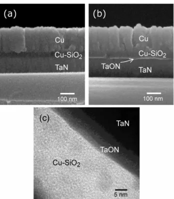
Fig. 11. (a) Cu/Cu-SiO2/TaN 以及(b) Cu/Cu-SiO2/TaON/TaN之截面圖,以及 Cu/Cu-SiO2/TaON/TaN電阻式記憶體之(c)雙極式 電阻切換 I-V 曲線,以及(d) ln I-V1/2與 ln I/V-V1/2曲線圖,與 100 次循環之 RHRS與 RLRS[31]
前述 5.1.3 節中的 Cu/Cu-SiO2/TaN 之電阻式記憶體可以進一步改善,使其同時具有高穩定性、較
低的 SET/RESET 電壓、高的RHRS/RLRS比值。前一節中的元件可能在 Cu-SiO2與TaN 交界面產生一層 不穩定的 TaON,因此此節特別控制界面結構。Fig. 11(a)為不使氧化物在 TaN 表面形成的狀況下,立 即沉積Cu-SiO2與 Cu 膜層之截面圖,顯現沒有額外氧化物薄膜生成;而此 Cu/Cu-SiO2/TaN元件的電 阻切換性質與前一節 Fig. 10 代表的第 20 次以後循環電阻切換結果相似[31]。Fig. 11(b)為刻意使氧化物 在 TaN 表面形成的狀況下,再鍍上Cu-SiO2與 Cu 膜層之截面圖,所添加氧化物膜層顯現較亮的影像 [31]。添加氧化物膜層之 Cu/Cu-SiO2/TaON/TaN 元件也具有雙極式電阻切換特性,如Fig. 11(c)所示其 SET 電壓約為+0.4 V 以及 RESET 電壓約為-0.2 V[31]。Fig. 11(c)的插圖顯示此元件的 LRS 仍為導電燈 絲,但 HRS 並不是空間電荷傳導機構;進一步以 ln I-V1/2方式比較結果如 Fig. 11(d),所得線性關係表 示 HRS 為蕭特基發射機構[31]。將此Cu/Cu-SiO2/TaON/TaN 元件進行 100 次電阻切換操作,再將各次 循環的 RHRS與RLRS收集得到結果如 Fig. 11(e),顯現 RHRS/RLRS比值皆超過 2 個數量級[31]。
此節得到的Cu/Cu-SiO2/TaON/TaN 元件具有與前述Cu/Cu-SiO2/Al 元件相似較高之 RHRS/RLRS比 值,但是所需的SET/RESET 電壓低,適合做為先進電阻式記憶體。
5.1.5. TaN/Cu-SiO2/TaN電阻式記憶體
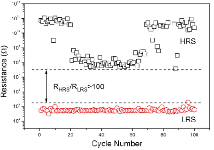
在以Cu-SiO2為電阻層的最後一種電阻式記憶體為 TaN/Cu-SiO2/TaN,這個主題的目的為除去循環 操作時容易造成可靠度問題的 Cu 上電極,由於本計畫規劃的電阻層內已經含有形成 Cu 燈絲的成分,
因此可以不需要活性 Cu 電極。Fig. 12(a)為此元件的截面圖,在控制鍍膜與儲存環境下所得到的三層 TaN/Cu-SiO2/TaN 結構間沒有額外氧化物生成。Fig. 12(c)的 I-V 曲線顯現此元件仍然具有雙極式電阻切 換特性;而其導電機構可以由 Fig. 12(d)的雙對數 I-V 曲線分析,其中 LRS 與 HRS 皆為空間電荷傳導 機構,此結果顯示於 LRS 時電阻層內沒有形成完整的導電燈絲,可能為間續的 Cu。最後分析元件進 行 100 次電阻切換操作之各次循環的 RHRS與RLRS值,結果如 Fig. 12(d),顯現 RHRS/RLRS比值稍微小於 1 個數量級[26]。未來可以調整參數使得 RHRS與RLRS比值增大,如此可使得此TaN/Cu-SiO2/TaN 元件 成為理想的電阻式記憶體。
(a) (b)
(c) (d)
Fig. 12. TaN/Cu-SiO2/TaN 元件之(a)截面圖,以及其(b)雙極式電阻切換 I-V 曲線,(c) ln I-V1/2與 ln I/V-V1/2曲線圖,與(d)100 次循環之 RHRS與 RLRS[26]
5.2 氧化鎳‒ 氧化鋯(NiO-ZrO2)複合膜電阻式記憶體
本計畫研究的第二類電阻膜層為NiO-ZrO2,為了瞭解複合膜對電阻切換特性的影響,本研究先以 純ZrO2膜層製做參考電阻式記憶體,再以NiO-ZrO2膜層製做電阻式記憶體比較。文獻中之ZrO2電阻 式記憶體主要以 Pt 為電極形成 Pt/ZrO2/Pt 或是 M/ZrO2/Pt 結構[19,20],少數文獻以 Al 為上下電極形成 Al/ZrO2/Al 結構[21]。本研究以 Al 為上下電極製做電阻式記憶體以避免使用昂貴的 Pt 電極,但仍可得 到單極式的電阻切換行為。
5.2.1. Al/ZrO2/Al電阻式記憶體
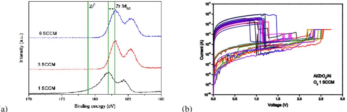
本研究以濺鍍法製備之ZrO2為缺氧狀態,Fig. 13(a)為以 XPS 分析鍍膜之 Zr 3d 束縛能,當鍍膜使 用的 O2流量為 1 sccm 得到較低之束縛能,O2流量為 6 sccm 得到接近計量型氧化鋯之束縛能(182.5-183 eV),因此缺氧程度隨氧氣流量降低而提高。使用定量 XPS 定量分析得到的成分結果依 O2流量為 1、3、
6 sccm 之條件,氧化鋯的組成為ZrO1.68、ZrO1.79、ZrO1.91。本研究之Al/ZrOx/Al 元件需先經過較高電 壓 Forming,之後可以進行電阻切換。如 Fig. 13(b)顯示之多次掃描得到的單極式 I-V 曲線,此以ZrO1.68
為電阻層之元件之 SET 電壓為+2.2 至+2.7 V,RESET 電壓為+0.8 至+2.0 V。
(a) (b)
Fig. 13. (a) ZrO2膜層之 Zr 3d 束縛能分析,以及(b) Al/ZrO2/Al 元件之單極式電阻切換 I-V 曲線
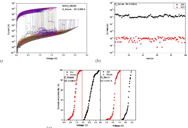
Fig. 14 (a)為電阻式記憶體進行 100 次循環掃描得到的 HRS 與 LRS 狀態的電流值,此樣品的電流 比值即等於 RHRS/RLRS值,此比值平均約可達 5 個數量級。但是這些電阻式記憶體有一個待解決的問題,
當循環掃描次數多時將 SET 電壓值與 RESET 電壓值統計,結果如 Fig. 14(b)顯示 SET 與 RESET 電壓 有重疊的區域,而且隨著鍍膜時 O2流量降低重疊情況愈嚴重,此行為將使Al/ZrO2/Al電阻式記憶體無 法正常操作電阻切換。
(a) (b)
Fig. 14. Al/ZrO2/Al 元件之(a)100 次循環之 HRS 與 LRS 電流值,以及(b)SET 與 RESET 電壓分布
5.2.2. Al/NiO-ZrO2/Al電阻式記憶體為
以混合NiO-ZrO2為電阻層之Al/NiO-ZrO2/Al 元件在經過 Forming 後的 I-V 掃描曲線如 Fig. 15(a),
由圖中可見元件顯現單極式電阻切換行為,而且其 SET 與 RESET 電壓可被區隔開。Fig. 15(b)為此元
件進行 100 次循環掃描得到的 HRS 與 LRS 狀態的電流值,平均約為 3 個數量級。Fig. 15(c)為電阻式記 憶體循環掃描 100 次統計的 SET 與 RSET 電壓,由圖中可看到Al/NiO-ZrO2/Al 元件之SET 與 RSET 電 壓不會重疊。
(a) (b)
(c)
Fig. 15. Al/NiO-ZrO2/Al 元件之(a)單極式電阻切換 I-V 曲線,(b)100 次循環之 HRS 與 LRS 電流值,以及(c)SET 與 RESET 電 壓分布
比較 5.2 節兩種元件的特性可知以NiO-ZrO2為電阻層之 Al/NiO-ZrO2/Al 元件雖然其 RHRS/RLRS值 比較低(但仍然超過 1000),但是其 SET 與RESET 電壓區間可以有效區隔開,適合作為電阻式記憶體。
另一方面,元件採用 Al 取代 Pt 為上下電極材質,可以使Al/NiO-ZrO2/Al電阻式記憶體實用化。
6. 結論與建議
本計畫研究以 Cu-SiO2為電阻膜之電阻式記憶體獲得以下成果:(1)以共濺鍍法製備之 Cu-SiO2為 膜應用於 Cu/Cu-SiO2/Pt 結構之電阻式記憶體元件時,不需要如文獻中進行預先以高電壓或高溫將 Cu 驅入 SiO2膜中,即可以具有可逆的雙極式電阻切換性質;(2)以 Al 與 TaN 取代昂貴的 Pt 下電極形成 Cu/Cu-SiO2/Al 與 Cu/Cu-SiO2/TaN,這兩種元件都可以具有可逆的雙極式電阻切換性質,顯示研究成果 可以與已發展的 IC 材料與製程相容;(3)添加 TaON 薄層製做的 Cu/Cu-SiO2/TaON/TaN 元件具有比較佳 的穩定性,以及較小的 SET 與 RESET 電壓,但是其 RHRS/RLRS比值仍需調高才符合未來記憶體使用。
(4) Cu 上電極也可以被置換為 TaN 以避免過多 Cu 導入電阻曾造成短路問題,此 TaN/Cu-SiO2/TaN 元件 也具有雙極式電阻切換特性。
本計畫研究以 NiO-ZrO2為電阻膜之電阻式記憶體獲得以下成果:(1)使用 Al 取代昂貴的 Pt 電極形 成的Al/ZrO2/Al 元件具有單極式電阻切換性質,其特性受到 ZrO2-x的缺氧狀態影響,雖然其 RHRS/RLRS
比值可以高達 5 個數量級,但是在 100 次循環操作下其 SET 與 RESET 電壓範圍局部重疊;(2) 以 NiO-ZrO2為電阻膜之Al/NiO-ZrO2/Al 元件也具有雙極式電阻切換性質,其 RHRS/RLRS比值約為 3 個數
量級,在 100 次循環操作下其 SET 與 RESET 電壓範圍已經可以分別開。
對於以 Cu-SiO2與NiO-ZrO2兩種材料為電阻層以及具經濟性與 IC 相容性的導體為電極材料,所 製做的元件都可以具有電阻切換性質,因此具有潛力以此類電阻式記憶體做為非揮發性記憶體。在以 Cu-SiO2為電阻層的方面可以持續往兩個方向研究:(1)在 Cu/Cu-SiO2/TaN 元件中添加均勻的界面氧化 物層以提高 RHRS/RLRS比值,以及元件操作的可靠度;(2)在 TaN/Cu-SiO2/TaN 元件中需調整電阻層內 之 Cu 含量,同時添加均勻的界面氧化物層,以提高元件操作的可靠度。在以 NiO-ZrO2為電阻層的方 面可以持續往兩個方向研究:(1)持續調整電阻層中NiO/ZrO2比例以及缺氧程度,使 SET 與 RESET 電 壓範圍已經可以有效分別開;(2)研究使用其他材料取代 Pt 電極,例如TaN/NiO-ZrO2/TaN 等等。
7. 計畫產出
7.1. SCI 期刊論文
(1) C.-J. Li, S. Jou, W.-L. Chen, “Resistance Switching of Copper-Doped Silica Films Grown by Sputter Deposition,” Jpn. J. Appl. Phys. 50 (2011) 01BG08. (附件 1)
(2) S. Jou, M.-E. Han, Jpn. J. Appl. Phys. (Submitted 2011). (附件 2)
7.2. 國際學術會議發表
(1) C.-J. Li, W.-L. Chen, S. Jou, 2010, “Resistance Switching of Copper-Doped Silica Films Grown by Sputter Deposition,” The Third International Symposim on Organic and Inorganic Electronic Materials and Related Nanotechnologies (EM-NANO 2010), Toyama, Japan, June 22-25, 2010.
(2) S. Jou, B.-R. Huang, C.-J. Li, “Resistance Switching Properties in Cu/Cu-SiO2/TaN Device,” World Congress on Engineering 2011, London, U. K., July 6-8, 2011, 1496-1499. (附件 3)
7.3. 專利
(1) S. Jou, C.-J. Li, “Method of Fabricating Variable Resistance Layer for Resistance Memory,” Korea Patent No. 1054465, August 4, 2011. (附件 4)
(2) (同一篇專利申請中) 周賢鎧,利嘉仁,“電阻式記憶體之可變電阻膜層的製造方法 Method of Fabricating Variable Resistance Layer for Resistance Memory”,中華民國專利,US Patent,JP Patent,
(2010)(台科大編號 980072)。
7.4. 學生學位論文
(1) 利嘉仁,「共濺鍍法沉積銅摻雜二氧化矽薄膜的電阻切換特性之研究」,碩士論文,台灣科技大學,
2010 年 7 月。
(2) 韓明恩,「界面氮氧化鉭氧化層對銅摻雜二氧化矽電阻切換性質的影響」,碩士論文,台灣科技大學,
2011 年 6 月。
(3) 栗漢翔,「共濺鍍法沉積氧化鎳‒ 氧化鋯複合薄膜的電阻切換特性研究」,碩士論文,台灣科技大學,
2011 年(準備中)。
參考文獻
[1] E. Linn, R. Rosezin, C. Kügeler, R. Waser, Nature Mater. 9 (2010) 403–406.
[2] C.-J. Wang, S. Jou, J. Phys. Chem. Solids 69 (2008) 523-526.
[3] 王貞芮,「添加銅之二氧化矽複合薄膜之研究」,碩士論文,台灣科技大學,2006 年。
[4] S. Jou, T.-H. Wu, J. Phys. Chem. Solids 69 (2008) 2804-2812.
[5] 吳姿慧,「以共濺鍍法製備固態氧化物燃料電池之鎳-氧化鋯陽極薄膜研究」,碩士論文,台灣科技 大學,2006 年。
[6] A. Sawa, Mater. Today 11 (2008) 28-36.
[7] C. Schindler, S. C. P. Thermadam, R. Waser, and M. N. Kozicki, IEEE Trans. Electron Devices 54 (2007) 2762-2768.
[8] C. Schindler, G. Staikov, R. Waser, Appl. Phys. Lett. 94 (2009) 072109.
[9] W. Guan, M. Liu, S. Long, Q. Liu, W. Wang, Appl. Phys. Lett. 93 (2008) 223506.
[10] D. Lee, D.-J. Seong, H. J. Choi, I. Jo, R. Dong, W. Xiang, S. Oh, M. Pyun, S.-O. Seo, S. Heo, M. Jo, D.-K. Hwang, H. K. Park, M. Chang, M. Hasan and H. Hwang, IEDM (2006) 346733.
[11] M. N. Kozicki, C. Gopalan, M. Balakrishnan and M. Mitkova, IEEE Trans. Nanotechnol. 5 (2006) 535-544.
[12] S.P. Thermadam, S.K. Bhagat, T.L. Alford, Y. Sakaguchi, M.N. Kozicki, M. Mitkova, Thin Solid Films 518 (2010) 3293-3298.
[13] W. Guan, S. Long, Q. Liu, M. Liu, W. Wang, IEEE Electron Device Lett. 29 (2008) 434-437.
[14] J. F. Gibbsons, W. E. Beadle, Solid State Electron. 7 (1964) 785-797.
[15] G.-S. Park, X.-S. Li, D.-C. Kim, R.-J. Jung, M.-J. Lee, and S. Seo, Appl. Phys. Lett. 91 (2007) 222103.
[16] K. Kinoshita, T. Tamura, M. Aoki, Y. Sungiyama, H. Tanaka, Jpn. J. Appl. Phys. 45 (2006) L991-L994.
[17] S.-E. Ahn, M.-J. Lee, Y. Park, B. S. Kang, C. B. Lee, K. H. Kim, S. Seo, D.-S. Suh, D.-C. Kim, J. Hur, W. Xianyu, G. Stefanovich, H. Yin, I.-K. Yoo, J.-H. Lee, J.-B. Park and B. H. Park, Adv. Mater. 20 (2008) 924-928.
[18] K. Tsunoda, K. Kinoshita, H. Noshiro, Y. Yamazaki, T. Iizuka, Y. Ito, A. Takahashi, A. Okano, Y. Sato, T.
Fukano, M. Aoki, Y. Sugiyama, IEDM (2007) 767-770.
[19] C. Y. Lin, C.-Y. Wu, C.-Y. Wu, C.-C. Lin, T.-Y. Tseng, Thin Solid Films 516 (2007) 444-448.
[20] C.-Y. Lin, C.-Y. Wu, C.-Y. Wu, T.-C. Lee, F.-L. Yang, C. Hu, T.-Y. Tseng, IEEE Electron. Device Lett.
28 (2007) 366-368.
[21] X. Wu, P. Zhou, J. Li, L. Y. Chen, H. B. Lv, Y. Y. Lin, T. A. Tang, Appl. Phys. Lett. 90 (2007) 183507.
[22] C.-C. Lin, J.-S. Yu, C.-Y. Lin, C.-H. Lin, T.-Y. Tseng, Thin Solid Films 516 (2007) 402-406.
[23] C.-Y. Lin, C.-C. Lin, C.-H. Huang, C.-H. Lin, T.-Y. Tseng, Surf. Coat. Technol. 202 (2007) 1319-1322.
[24] S. Jou, B.-R. Huang, C.-J. Li, World Congress on Engineering 2011, London, U. K., July 6-8, 2011, 1496-1499.
[25] 周賢鎧,「混合氧化物薄膜之電阻切換性質與微結構研究」,國科會專題研究計畫書 NSC 98-2221-E-011-040-MY2,2009 年。
[26] 韓明恩,「界面氮氧化鉭氧化層對銅摻雜二氧化矽電阻切換性質的影響」,碩士論文,台灣科技大 學,2011 年。
[27] 利嘉仁,「共濺鍍法沉積銅摻雜二氧化矽薄膜的電阻切換特性之研究」,碩士論文,台灣科技大學,
2010 年。
[28] C.-J. Li, S. Jou, W.-L. Chen, Jpn. J. Appl. Phys. 50 (2011) 01BG08.
[29] A.E. Rakhshani, J. Appl. Phys. 69 (1991) 2365-2369.
[30] Y. Xia, W. He, L. Chen, X. Meng, Z. Liu, Appl. Phys. Lett. 90 (2007) 022907.
[31] S. Jou, M.-E. Han, Jpn. J. Appl. Phys. (Submitted 2011).
[32] N. Nagashima, T. Yanagida, K. Oka, T. Kawai, Appl. Phys. Lett. 94 (2009) 242902.
附件 1
附件 2 (Submitted to Japanese Journal of Applied Physics, 2011)
Influence of interfacial tantalum oxynitride to resistive switching of Cu/Cu‒ SiO2/TaN Shyankay Jou* and Ming-En Han
Department of Materials Science and Engineering, National Taiwan University of Science and Technology, Taipei 106, Taiwan, R. O. C.
Reversible switching of resistance of Cu/Cu‒ SiO2/TaN cells between high resistance state (HRS) and low resistance state (LRS) were studied. A Cu‒ SiO2 layer of about 40 nm thick was utilized as the resistor layer. Top and bottom electrode were made of Cu and TaN of about 160 and 110 nm thick, respectively. The cells were constructed with a cross bar structure with an area of 50 × 50 μm2. The Cu/Cu‒ SiO2/TaN cell exhibited bipolar switching of resistance with set voltages around +1.0 V, reset voltages around ‒ 0.6 V, and resistance ratios (RHRS/RLRS) about 6 to 8. By inserting a thin TaON layer between the Cu‒ SiO2 and TaN in the cell, RHRS/RLRS was increased to above 400, and set and reset voltages were about +0.3 V and ‒ 0.2 V, respectively. The conduction mechanisms for the Cu/Cu‒ SiO2/TaN cells with and without an interfacial TaON layer were discussed.
*E-mail address: [email protected].
1. Introduction
Resistive random access memory (RRAM) has been extensively studied due to its potential application in future nonvolatile memory.1) Various oxides have shown resistance switching under voltage sweeps.2) For example, copper-doped oxides such as Cu‒ MoO3, Cu‒ WO3, Cu‒ ZrO2 and Cu‒ SiO2 have exhibited bipolar switching of resistance featuring electrochemical
metallization of Cu.3‒ 12) The change between low resistive state (LRS) and high resistive state (HRS) of these RRAM of copper-doped oxides accompanied with formation and rupture of conductive filaments inside the oxide films.3‒ 9) In this regards, copper-doped-oxide based RRAM was usually composed of an active Cu electrode and an inert Pt electrode.3‒ 6,9,11) Replacement of the inert Pt electrode with less expensive materials such as tungsten has been reported.7,8) In a previous work, we have utilized Al as an inert electrode to facilitate bipolar switching of Cu‒ SiO2 RRAM.11) The Cu/Cu‒ SiO2/Al cell had a resistance ratio (RHRS/RLRS) of 7990, as compared with that of about 100 for the Cu/Cu‒ SiO2/Pt cell. And electrical conduction for the cells in HRS changed from the space-charge-limit-current (SCLC), a bulk-limited mechanism, for Cu/Cu‒ SiO2/Pt cell to Schottky emission, an electrode-limited mechanism, for Cu/Cu‒ SiO2/Al cell. The high ratio of RHRS/RLRS and the electrode-limited conduction mechanism for the cell utilizing Al as the inert electrode was attributed to a the presence of a thin native oxide layer on the surface of the Al electrode.11) Recently, we have utilized TaN as an inert electrode and demonstrated bipolar switching of
Cu/Cu‒ SiO2/TaN cell.12) The Cu/Cu‒ SiO2/TaN cell in HRS exhibited Schottky emission in first few cycles of resistive switching and then changed to SCLC after several cycles of switching. And RHRS/RLRS ratios decreased from above 90 in first few cycles of switching to about 5 after 25 cycles of switching. The changes of conduction mechanisms and resistance ratios with cycles of switching were due to instable oxide film that was spontaneously formed on the surface of the TaN electrode during preparation of the Cu/Cu‒ SiO2/TaN RRAM cell.
In this study, we investigated RRAM of Cu/Cu‒ SiO2/TaN with intentional control of the interface between the TaN electrode and the Cu‒ SiO2 film. A clean TaN surface, without an oxide film, was obtained by limiting exposure of specimen to air before depositing Cu‒ SiO2 film. On the other hand, an oxide layer was generated on the surface of TaN by a plasma oxidation procedure before depositing Cu‒ SiO2 film. Both RRAM cells showed bipolar switching of resistance but with different conduction
mechanisms in HRS. The roles of the interfacial TaON on the switching properties of Cu/Cu‒ SiO2/TaN cells were discussed.
2. Experimental Procedure
A resistor layer of about 40 nm thick was prepared by co-sputter deposition of a Cu target and a SiO2 target. Details of deposition conditions were described elsewhere.11) The resistor layer was composed of Cu2O clusters in a SiO2 matrix,11,13) and the atomic ratio of Cu:Si determined by X-ray photoelectron spectroscopy was 9.9: 90.1 in current study. In order to make the RRAM cell, a crossbar metal-oxide-metal (MOM) structure with an area of 50 × 50 μm2 was fabricated by sequential sputter depositions of TaN, Cu‒ SiO2, and Cu through metal masks on a Si(100) substrate with a 500-nm-thick thermal oxide.11,12) The TaN bottom electrode (BE) was deposited by reactive sputter of a Ta target (99.99%) in a mixed flow of 10 cm3/min of Ar (99.9995%) and 1 cm3/min of N2 (99.999%), with a working pressure of 1.2 Pa. The Cu top electrode (TE) was deposited by sputtering a Cu target (99.999%) in a flow of 10 cm3/min of Ar with a working pressure of 1.2 Pa.
Two RRAM cells, Cu/Cu‒ SiO2/TaN and Cu/Cu‒ SiO2/TaON/TaN, were compared in this study. The exposure time in air ambient before depositing the Cu‒ SiO2 layer was limited to 2 min to prevent formation of a native oxide layer on the surface of the TaN bottom electrode during preparation of the first cell. On the contrary, the surface of the TaN electrode was oxidized to form a stable oxide layer before depositing Cu‒ SiO2 in the second cell. The oxidation was conducted by exposing the TaN electrode in a mixed Ar and O2 (99.999%) plasma with an r.f. power of 100 W for 10 min.
Cross section of the cells was inspected by scanning electron microscopy (SEM, JEOL JSM-6500F). Interface structure of the cell with surface-oxidized TaN electrode was inspected by transmission electron microscopy (TEM, Philips Tecnai G2 F20 TEM). Current-voltage (I‒ V) characteristic of the MOM cells was measured by Agilent B1500A through attaching tungsten probes to the electrode pads which were extended from the crossbar structure. The bottom electrode was grounded, and voltage
sweeps were applied to the top electrode.
3. Results and Discussion
Cross-sectional SEM images of the Cu/Cu‒ SiO2/TaN and Cu/Cu‒ SiO2/TaON/TaN cells are displayed in Fig. 1(a) and 1(b).
Thicknesses of the Cu top electrode, Cu‒ SiO2 resistor layer, and TaN bottom electrode are about 160, 40, and 110 nm, respectively.
The interface between Cu‒ SiO2 and TaN in the Cu/Cu‒ SiO2/TaN cell, the cell without intentionally oxidizing the TaN electrode, has no additional substance. On the other hand, there is a thin layer of substance between Cu‒ SiO2 and TaN in the
Cu/Cu‒ SiO2/TaON/TaN cell, the cell with intentionally oxidizing the surface of the TaN bottom electrode. The interfacial TaON film is about 10 nm thick, as displayed in Fig. 1(c) of cross-sectional TEM image.
Figure 2 shows hysteresis I‒ V curves for the Cu/Cu‒ SiO2/TaN cell in its first and the 28th cycles of voltage sweep. This cell instantly exhibits bipolar switching in counterclockwise direction, having no need of a prior forming step to generate an initial conductive path at high temperatures7,8) or high voltages.4,11) The SET voltage for switching from HRS to LRS is about +1.0 V where the current increases to a compliant limit of 10‒ 5 A. The cell remains LRS until the voltage is swept in opposite polarity to the a RESET voltage of ‒ 0.6 V. The cell can be reversibly switched for several cycles. Inset at Fig. 2 displays logarithmic plot of the I‒ V curve for the Cu/Cu‒ SiO2/TaN cell in the first cycle of switch. The lower curve for HRS can be divided into three regions with slopes of 1.07, 2.07 and 4, respectively. The combined slope values at different voltages represents the
trap-controlled SCLC mechanism, featuring Ohmic conduction (I∞V) at low voltages, Child’s square law (I∞V2) at medium voltages and the trap-controlled behavior (I∞Vn, n>2) at high voltages.3,14‒ 19) Therefore, electrical conduction for the Cu/Cu‒ SiO2/TaN cell in HRS in this study is a bulk-limited process, in which charge carriers and defects in insulator governs electrical conduction.15,19) Meanwhile, resistance values of the Cu/Cu‒ SiO2/TaN cell in HRS (RHRS) and LRS (RLRS) were
recorded at +0.2 V and displayed in Fig. 3. The ratios of RHRS/RLRS for the Cu/Cu‒ SiO2/TaN cell in this study are between 6 and 8 in 30 cycles of resistance switch. These ratios are similar to those observed in a similar cell but with a spontaneously formed thin interfacial oxide layer after it was cyclically switched for more than 20 times in a previous study.11) In comparison with
performance of the previous cell,12) the Cu/Cu‒ SiO2/TaN cell in this study has stable resistance switching properties due to lack of an instable interfacial oxide layer.
On the other hand, the Cu/Cu‒ SiO2/TaON/TaN cell showed resistance switching only after a forming process at +4V was conducted. Figure 4 shows the I‒ V curves for the Cu/Cu‒ SiO2/TaON/TaN cell in the 99th and 100th cycles of resistance switch.
This cell exhibits bipolar switching behavior with clear SET and RESET processes. The cell abruptly changes from HRS to LRS at about +0.3 to +0.4 V, and changes back from LRS to HRS at about ‒ 0.2 V. Inset at Fig. 4 displays a logarithmic plot of I‒ V curve for the Cu/Cu‒ SiO2/TaON/TaN cell in the 99th cycle of switch. The lower curve for HRS does not have a linear region showing slope value of 1 or 2. Therefore, conduction mechanism other than SCLC governs electric conduction in HRS of this cell.
Figures 5(a) and 5(b) show plot of ln I against V1/2 in low voltage region and ln I/V against V1/2 in high voltage region for HRS of this cell, respectively. Both plots are linear and, therefore, the electric conduction in HRS follows Schottky emission in low voltages and Poole-Frenkle mechanism in high voltages.15,20) The TaON interfacial layer in the Cu/Cu‒ SiO2/TaON/TaN cell caused Schottky emission, which is an electrode-barrier-limited conduction process.15,20) Meanwhile, the ratios of RHRS/RLRS
measured at +0.2 V are between 400 and 300000 for 100 cycles of resistance switching, as shown in Fig. 6. As a result, the implementation of a TaON interfacial film provided high RHRS/RLRS ratio for the Cu/Cu‒ SiO2/TaON/TaN cell, as compared to the low RHRS/RLRS ratio for the Cu/Cu‒ SiO2/TaN cell without an interfacial TaON film. On the other hand, RHRS/RLRS ratios greater than 400 remain in the Cu/Cu‒ SiO2/TaON/TaN cell for 100 cycles of resistance switching in this study. It is contrary to the instable switching behavior in a similar cell with spontaneously formed oxide layer in a previous study.12) In like manner, various interfacial oxide layers between an electrode and an insulator have been found to improve performance of RRAM cells.9,21,22) The interfacial TaON layer herein increased stability and RHRS/RLRS ratio for the Cu‒ SiO2‒ based RRAM cell.
In comparison with instable switch behavior of Cu/Cu‒ SiO2/TaN in a previous study,12) both Cu/Cu‒ SiO2/TaN and
Cu/Cu‒ SiO2/TaON/TaN cells in current study showed stable resistance switch. The previous Cu/Cu‒ SiO2/TaN cell might have an ultra-thin oxide layer spontaneously grown on the surface of TaN electrode due to uncontrolled air exposure. That thin TaON layer was possibly reduced back to TaN by reaction with oxygen-deficient SiOx in Cu‒ SiO2 layer during cycles of resistance switch.12) Thus the resistance in HRS corresponding to a Cu/Cu‒ SiO2/TaON/TaN structure was high at the beginning but decreased with cycle times, and eventually reached a low resistance value corresponding to a Cu/Cu‒ SiO2/TaN structure in the previous study.12) In current study, the time for air exposure for the Cu/Cu‒ SiO2/TaN cell was limit so that an interfacial TaON layer was not present.
Therefore, the Cu/Cu‒ SiO2/TaN cell exhibit stable resistance switching with low RHRS/RLRS ratios due to lack of instable interfacial oxide layer. For the Cu/Cu‒ SiO2/TaON/TaN cell, about 10 nm of TaON layer was intentionally grown on the surface of the TaN electrode. The TaON layer was stable and, therefore, the Cu/Cu‒ SiO2/TaN cell exhibit stable resistance switching with high RHRS/RLRS ratios.
4. Conclusions
In summary, bipolar switching of RRAM of Cu/Cu‒ SiO2/TaN and Cu/Cu‒ SiO2/TaON/TaN were demonstrated. The intentionally introduced TaON layer between the TaN bottom electrode and the Cu‒ SiO2 resistor increased resistance ratio of RHRS/RLRS to a value of above 400. The conduction mechanism was Schottky emission for the RRAM cell with the presence of an interfacial TaON layer, and was SCLC for the cell without an interfacial oxide layer.
Acknowledgement
This work was supported by the R.O.C. National Science Council through the grant NSC-98-2221-E-011-040-MY2.
1) R. Waser, R. Dittmann, G. Staikov, and K. Szot: Adv. Mater. 21 (2009) 2632.
2) A. Sawa, Mater. Today 11, 28 (2008).
3) D. Lee, D.-J. Seong, I. Jo, X. R. Dong, S. Oh, and H. Hwang: Appl. Phys. Lett. 90 (2007) 122104.
4) C. Schindler, G. Staikov, and R. Waser: Appl. Phys. Lett. 94 (2009) 072109.
5) W. Guan, S. Long, Q. Liu, M. Liu, and W. Wang: IEEE Electron. Device Lett. 29 (2008) 434.
6) W. Guan, M. Liu, S. Long, Q. Liu, and W. Wang: Appl. Phys. Lett., 93 (2008) 223506.
7) C. Schindler, S. C. P. Thermadam, R. Waser, and M. N. Kozicki: IEEE Trans. Electron Devices 54 (2007) 2762.
8) S. P. Thermadam, S. K. Bhagat, T. L. Alford, Y. Sakaguchi, M. N. Kozicki, and M. Mitkova: Thin Solid Films 518 (2010) 3293.
9) J. Yoon, J. Lee, H. Choi, J.-B. Park, D.-J. Seong, W. Lee, C. Cho, S. Kim, and H. Hwang: Microelectron. Eng. 86 (2009) 1929.
10) M. N. Kozicki, C. Copalan, M. Balarkrishnan, and M. Mitkova: IEEE Trans. Nanotechnol. 5 (2006) 535.
11) C.-J. Li, S. Jou, and W.-L. Chen: Jpn. J. Appl. Phys. 50 (2011) 01BG08.
12) S. Jou, B.-R. Huang, and C.-J. Li: Proc. Word Congress on Engineering, Vol II, 2011, p. 1496.
13) C.-J. Wang and S. Jou: J. Phys. Chem. Solids 69 (2008) 23.
14) A. E. Rakhashani: J. Appl. Phys. 69 (1991) 2365.
15) G. R. Fox and S. B. Krupanidhi: J. Appl. Phys. 74 (1993) 1949.
16) S. Kim, H. Y. Jeong, S. Y. Choi, and Y.-K. Choi: Appl. Phys. Lett. 97 (2010) 033508.
17) A. Chen, S. Haddad, Y.-C. Wu, T.-N. Fang, Z. Lan, S. Avanzino, S. Pangrle, M. Buynoski, M. Rathor, W. Cai, N. Tripsas, C.
Bill, M. VanBuskirk, and M. Taguchi: IEDM2005, 746.
18) C.-Y. Liu, and J.-M. Hsu: Jpn. J. Appl. Phys. 49 (2010) 084202.
19) C. Sudhama, A. C. Campbell, P. D. Maniar, R. E. Jones, R. Moazzami, C. J. Mogab, and J. C. Lee: J. Appl. Phys. 75 (1994) 1014.
Y. Xia, W, He, L. Chen, X. Meng, and Z. Liu: Appl. Phys Lett. 90 (2007) 022907.
20) P. C. Joshi and S. B. Krupanidhi: J. Appl. Phys. 73 (1993) 7627.
21) P. Zhou, M. Yin, H. J. Wan, H. B. Lu, T. A. Tang, and Y. Y. Lin: Appl. Phys. Lett. 94 (2009) 053510.
22) J. S. Kwak, Y. H. Do, Y. C. Bae, H. S. Im, J. H. Yoo, M. G. Sung, and Y. T. Hwang, J. P. Hong: Appl. Phys. Lett. 96 (2010) 223502.
Fig. 1. Cross sections of (a) Cu/Cu‒ SiO2/TaN cell and (b) Cu/Cu‒ SiO2/TaON/TaN cell. (c) TEM image for interfacial region of Cu‒ SiO2/TaON/TaN.
Fig. 2. Current-voltage characteristics of the Cu/Cu‒ SiO2/TaN cell in the first and the 28th cycles of resistance switch.
The Inset shows logarithmic plot of I‒ V curve for LRS and HRS in the first cycle of resistance switch.
Fig. 3. Plot of resistance against cycle numbers in HRS and LRS for the Cu/Cu‒ SiO2/TaN cell.
Fig. 4. Current-voltage characteristics of the Cu/Cu‒ SiO2/TaON/TaN cell in the 99th and 100th cycles of resistance switch.
The Inset shows logarithmic plot of I‒ V curve for LRS and HRS in the first cycle of resistance switch.
Fig. 5. Plots of (a) ln I against V1/2 and (b) ln I/V against V1/2 for HRS for the Cu/Cu‒ SiO2/TaON/TaN cell in the 99th cycle of resistance switch.
Fig. 6. Plot of resistance against cycle numbers in HRS and LRS for the Cu/Cu‒ SiO2/TaON/TaN cell.
附件 3
附件 4
![Fig. 2. 電阻式記憶體的(a)單極式切換,以及(b)雙極式電阻切換的 I-V 特性曲線[6]](https://thumb-ap.123doks.com/thumbv2/9libinfo/9125503.409899/4.892.72.817.62.482/Fig2電阻式記憶體的a單極式切換以及b雙極式電阻切換的特性曲線.webp)
![Fig. 4. 本計畫電阻式記憶體 MIM 構造之(a)上視圖與(b)截面示意圖[24]](https://thumb-ap.123doks.com/thumbv2/9libinfo/9125503.409899/5.892.237.675.758.976/Fig4本計畫電阻式記憶體MIM構造之a上視圖與b截面示意圖24.webp)
![Fig. 7. Cu/Cu-SiO 2 /Pt 標準電阻式記憶體之(a)截面圖[27],(b)雙極式電阻切換 I-V 曲線[28],以及比教導電機構之雙對數 I-V 曲線圖[28]](https://thumb-ap.123doks.com/thumbv2/9libinfo/9125503.409899/7.892.80.841.838.1028/FigCuCuSiOPt標準電阻式記憶體截面雙極式電阻切曲線及比教導電機構之.webp)
![Fig. 8. Cu/Cu-SiO 2 /Al 電阻式記憶體之 (a)雙極式電阻切換 I-V 曲線,以及比教導電機構之(b)雙對數 I-V 曲線圖,(c) ln I-V 1/2 曲線,以及(d)界面之高解析度截面圖[27,28]](https://thumb-ap.123doks.com/thumbv2/9libinfo/9125503.409899/8.892.199.708.365.760/FigCuCuSiOAl電阻式記憶體雙極式電阻切曲線以及比教導電機構雙對曲線.webp)
![Fig. 9. Cu/Cu-SiO 2 /TaN 電阻式記憶體第 5 次循環之(a)雙極式電阻切換 I-V 曲線,比教導電機構之(b)雙對數 I-V 曲線圖,以 及(c) ln I-V 1/2 曲線[24]](https://thumb-ap.123doks.com/thumbv2/9libinfo/9125503.409899/9.892.75.842.76.274/FigCuCuSiOTaN電阻式記憶體次循環之雙極式電阻切曲線比教導電機構雙對.webp)
![Fig. 12. TaN/Cu-SiO 2 /TaN 元件之(a)截面圖,以及其(b)雙極式電阻切換 I-V 曲線,(c) ln I-V 1/2 與 ln I/V-V 1/2 曲線圖,與(d)100 次循環之 R HRS 與 R LRS [26]](https://thumb-ap.123doks.com/thumbv2/9libinfo/9125503.409899/10.892.152.754.701.1110/Fig1TaNCuSiOTaN件之截面圖以及其雙極式電阻切曲線曲線圖與次循環之與.webp)