attributed to the formation of a Ta2O5共or TaOx) layer at the Cu(Ta)/SiO2interface, as revealed by X-ray photoelectron spectros-copy analysis. The connections between the Ta alloying contents and the microstructural as well as the interfacial characteristics of Cu on SiO2are discussed.
© 2003 The Electrochemical Society. 关DOI: 10.1149/1.1630597兴 All rights reserved.
Manuscript submitted March 19, 2003; revised manuscript received July 15, 2003. Available electronically November 21, 2003.
For the modern ultra-large-scale integration共ULSI兲 circuits, the copper interconnect has received considerable attention because of its lower resistivity共⬃1.7 ⍀ cm for bulk兲 and superior resistance to electromigration than the conventional Al-based interconnects.1 However, copper suffers from disadvantages such as poor adhesion to SiO2and fast diffusion into Si2and SiO2.3Thus, the addition of alloying elements may overcome these drawbacks. Alloying copper with some extra elements may improve its adhesion to SiO2,4,6 promote its oxidation resistance,5,6 enhance the electromigration resistance,7and retard the diffusion of Cu into SiO2.8,9
Some alloying elements, such as Ta, V, Nb, Cr, Mo, Fe, Ru, and Ag, have no or limited solid solubility with Cu at elevated tempera-ture. The dissociation and electric resistivity of these eight dilute Cu alloys were reported.10 The additive elements in these immiscible Cu alloys are expected to segregate at grain boundaries, free sur-faces, or interfaces. In view of materials science, the segregation may result in the retention of the perfect conductivity of copper, as well as the inhibition of atomic diffusion and oxidation of copper. Among these immiscible elements, Ta is the most interesting addi-tive element because it is currently a major material in ULSI cir-cuits, such as the TaNx11,12and Ta12,13diffusion barriers.
Wang et al. reported that the microstructure of Cu-Ta alloy film, 12m thick, remained submicrometer grain size and the Ta particles precipitated to grain boundary after annealing at 900°C.14However, as an interconnect material, there is no detailed literature regarding the interfacial reaction and diffusion of Cu-Ta alloy films关referred to as Cu共Ta兲 hereafter兴 with its neighboring materials. The diffusion of Cu into SiO2may cause degradation of devices at high tempera-ture or high voltage. Therefore, in this work, pure Cu and Cu共Ta兲 alloy thin films were deposited on SiO2/具Si典substrates共具Si典 repre-sents the single crystal wafer兲 and subsequently annealed. The ob-jective of this study was to investigate how the Ta content affects the interfacial reaction and/or interdiffusion of Cu共Ta兲 films with SiO2. Characteristics of the Cu(Ta)/SiO2/具Si典 and Cu/SiO2/具Si典 multilayer stacks, such as electrical resistivity and microstructural evolution, are also studied.
Experimental
Cu and two Cu共Ta兲 films were deposited onto 270 nm of thermal SiO2 covered n-type Si substrate by magnetron sputtering. The Cu共Ta兲 films were prepared by cosputtering from a Cu target 共99.99% purity兲 and a Ta target 共99.95% purity兲. A negative dc bias of 150 V was applied to the substrate during deposition. Base pres-sure of the chamber was 2.5⫻ 10⫺6Torr and working pressure was 4 mTorr. The Ta contents of two Cu-Ta alloy films investigated in the present work were determined by electron probe microanalyzer 共EPMA, JEOL 8900R兲 and they are 0.1 atom % 关referred to as Cu共0.1 atom % Ta兲兴 and 2.3 atom % 关referred to as Cu共2.3 atom % Ta兲兴. Thicknesses of pure Cu, Cu共0.1 atom % Ta兲, and Cu共2.3 atom % Ta兲 films were measured by profilometer 共Tencor ␣-step兲 and they are 170, 145, and 150 nm, respectively. After deposition, all samples were annealed in vacuum at a pressure of 2⫻ 10⫺5 Torr. The an-nealing temperature was ranging from 500 to 800°C and the dura-tion was 30 min.
Resistivity of pure Cu and Cu共Ta兲 films was calculated from the sheet resistance measured with a four-point probe and the film thick-ness. The characteristic phases in the samples were identified by using Bragg-Brentano diffractometry, also termed-2 X-ray dif-fraction共-2 XRD, Rigaku D-Max-IV兲, with Cu K␣ radiation. Sur-face morphology was examined with scanning electron microscopy 共SEM, Philips XL-40FEG兲, which utilizes a secondary electron sig-nal to produce the image. Transmission electron microscopy共TEM, Hitachi HF-200兲 was employed to examine the grain microstructure of the films. Interfacial reaction was analyzed with X-ray photoelec-tron spectroscopy共XPS, VG ESCA 210兲. The original spectra were smoothed first and then a linear background was subtracted before the deconvolution carried out. Deconvolution of XPS data was done by fitting the spectra to multiple peaks of Gaussian functions with required intensity ratio (I4f 7/2:I4f 5/2⫽ 4:3).15 Compositional depth profile analysis was performed by using Rutherford back-scattering spectrometry共RBS兲 with 2 MeV He⫹beams.
Results and Discussion
Resistivity values of Cu, Cu共0.1 atom % Ta兲 and Cu共2.3 atom % Ta兲 films, as a function of annealing temperature, are shown in Fig. 1. For every sample, the resistivity value is the average of five measurements and the error bar indicates the difference of the max⫺ min. The resistivity of as-deposited Cu, Cu共0.1 atom % Ta兲 and Cu共2.3 atom % Ta兲 are about 1.97, 6.25, and 31.2 ⍀ cm, respectively. This result shows that the resistivity of as-deposited *Electrochemical Society Active Member.
Cu共Ta兲 films increased as the Ta additives increased. A similar result was observed by Barmak et al.10They reported that the resistivity of as-deposited Cu共2.8 atom % Ta兲 film was about 42 ⍀ cm. After annealing at 500-800°C, the resistivity of all films decreases, but the reduction was the most significant for Cu共2.3 atom % Ta兲. Resistiv-ity of the 800°C annealed Cu共2.3 atom % Ta兲 film is only about one sixth of the as-deposited Cu共2.3 atom % Ta兲 film. Compared to pure Cu, the decrease of resistivity for Cu共Ta兲 is large, especially for the Cu共2.3 atom % Ta兲. Lowering of the resistivity may be attributed to out-diffusion of additive atoms, annihilation of defects and grain growth of films. The small drop in resistivity of the pure Cu film suggests that the defect annihilation and grain growth may have a relatively minor effect on the decrease of resistivity. As a result, the concentration of Ta located within the crystal lattices of Cu共Ta兲 films should decrease upon annealing, possibly by out diffusion of Ta additives.
However, compared to the pure Cu film, the resistivity of an-nealed Cu共Ta兲 films is still high. This may be attributed to the fol-lowing factors. First, some Ta atoms may segregate to the grain boundaries but are still located within the Cu layer. Second, the crystal lattices of annealed Cu共Ta兲 films may still contain residual Ta or inhibit the grain growth. To further understand the difference in the resistivity variation, material characteristics of the samples upon vacuum annealing were examined as follows.
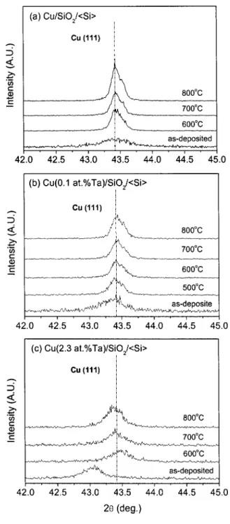
-2 XRD was employed to identify the phases present in the samples before and after annealing at 500-800°C. XRD patterns of Cu, Cu共0.1 atom % Ta兲, and Cu共2.3 atom % Ta兲 samples show all face-centered cubic共fcc兲 Cu peaks only, without detection of Ta or other phase. However, the positions of fcc Cu共111兲 peaks reflected different interplanar spacings for pure Cu and Cu共Ta兲 films. Figure 2 shows the XRD patterns of Cu共111兲 peaks for pure Cu, Cu共0.1 atom % Ta兲, and Cu共2.3 atom % Ta兲 samples, before and after annealing. Si powders were used as the standard sample to correct the diffrac-tion peak posidiffrac-tions. From Fig. 2, it is apparent that the Cu共111兲 peak of the as-deposited Cu共2.3 atom % Ta兲 sample shifted to a lower angle共⫺0.33°兲 relative to that of as-deposited pure Cu, indicating that the presence of Ta additive atoms causes the expansion of the Cu lattice. A similar result was reported by Chu et al.16They re-ported that in the Cu-Mo system共Mo contents ranging form 2 to 25 atom %兲, the Cu共111兲 peaks of as-deposited Cu共Mo兲 films moved to lower angles. Because the solid solubility of Ta in Cu is negligible,17 the XRD analysis indicates that a nonequilibrium, super-saturated Cu共Ta兲 solid solution is formed by cosputtering deposition.
After annealing, the Cu共111兲 peak position of the Cu(2.3 atom % Ta)/SiO2/具Si典 system approached that of the Cu/SiO2/具Si典system. It implied that Ta additives had segregated to
the grain boundaries, surface, or interface upon annealing, which led to a comparable lattice spacing for Cu共2.3 atom % Ta兲 and pure Cu. In order to understand the effect of Ta additives in Cu on the mor-phological change, surfaces of all films were examined by SEM, before and after annealing.
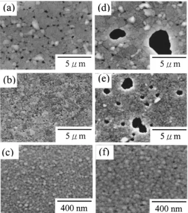
SEM micrographs on the surfaces of the as-deposited Cu/SiO2/具Si典, Cu(0.1 atom % Ta)/SiO2/具Si典, and Cu(2.3 atom % Ta)/SiO2/具Si典 samples are shown in Fig. 3. There is no significant difference in the surface morphology of the three samples. Small nodules are observed on the free surfaces and each nodule may be composed of one or several Cu grains. Figure 4 shows SEM micrographs on the surfaces of Cu/SiO2/具Si典, Figure 1. Variation of resistivity values with annealing temperature
for Cu/SiO2/具Si典, Cu(0.1 atom% Ta)/SiO2/具Si典, and Cu(2.3 atom% Ta)/ SiO2/具Si典samples.
Figure 2. -2 XRD patterns of 共a兲 Cu/SiO2/具Si典 共b兲
Cu(0.1 atom% Ta)/SiO2/具Si典, and 共c兲 Cu(2.3 atom% Ta)/SiO2/具Si典 samples, before and after annealing at 600°C, 700 and 800°C. The dash-dot line indicates the Cu共111兲 peak position of the pure Cu film, which is only 0.08° deviated from the ICDDPDF共04-0836兲 data.
Cu(0.1 atom % Ta)/SiO2/具Si典, and Cu(2.3 atom % Ta)/SiO2/具Si典 samples, after annealing at 700 and 800°C. Evident voids were seen on the 700°C annealed Cu surface共Fig. 4a兲. These voids indicated that the initiation of copper agglomeration and the exposed regions are the underlying SiO2layer. However, there was no void observed in the 700°C annealed Cu共0.1 atom % Ta兲 and Cu共2.3 atom % Ta兲 samples 共Fig. 4b, c兲. Surface morphology of the 700°C annealed Cu共2.3 atom % Ta兲 film was almost the same as that of as-deposited
Cu共2.3 atom % Ta兲 film 共Fig. 3c兲. After annealing at 800°C, the voids of Cu and Cu共0.1 atom % Ta兲 films 共Fig. 4d and e兲 were evident and coalesced to large broken holes. However, the 800°C annealed Cu共2.3 atom % Ta兲 film 共Fig. 4f兲 still remained a smooth surface. No voids are seen on the Cu共2.3 atom % Ta兲 surface even after annealing up to 800°C.
Agglomeration of polycrystalline thin films occurs via grain growth and nucleation of holes at grain-boundary vertices.18 There-fore, grain growth is a necessary step before agglomeration occurs. In order to understand the difference of grain sizes between Cu, Cu共0.1 atom % Ta兲, and Cu共2.3 atom % Ta兲 films after annealing, the grain sizes were estimated by applying Scherrer’s formula19to the Cu共111兲 diffraction peaks. After annealing at 700°C, the esti-mated grain sizes of Cu, Cu共0.1 atom % Ta兲, and Cu共2.3 atom % Ta兲 are 47, 42, and 27 nm, respectively.
Figure 5 shows the TEM planar-view micrographs of as-deposited and 700°C annealed Cu共2.3 atom % Ta兲 films. Obviously, the grain sizes of as-deposited and 700°C annealed Cu共2.3 atom % Ta兲 film were about the same. Therefore, the grains in the Cu共2.3 atom % Ta兲 film did not grow upon annealing. From the TEM mi-crograph, the average grain size of 700°C annealed Cu共2.3 atom % Ta兲 was 26 nm, which is very close to the estimated grain size calculated by Scherrer’s formula.
From the results shown above, we realize that the degree of grain growth decreased as the Ta additives increased. The very low degree of grain growth for the Cu共2.3 atom % Ta兲 system is attributed to the segregation of Ta atoms to the grain boundaries, which inhibit the movement of grain boundaries and consequently prevent the forma-tion of voids 共or holes兲. In addition, it has been reported that the segregated atoms stuff the grain boundaries and consequently de-crease the rate of electromigration of Cu atoms through grain bound-aries under a high electric field.20
To investigate the Cu(Ta)/SiO2 interfaces, we stripped the Cu共Ta兲 layers of the as-deposited and 700°C annealed samples by chemical solution共mixture of nitric acid, phosphoric acid, and acetic acid兲. The Cu films were etched by chemical solution, but the me-tallic Ta and Ta oxides were not. The exposed SiO2surface was than examined by using XPS. In addition, the compositional depth pro-files of as-deposited and 700°C annealed Cu, Cu共0.1 atom % Ta兲, and Cu共2.3 atom % Ta兲 systems were analyzed by using RBS. The 700°C annealed samples were selected because the Cu surfaces re-mained mostly continuous expect for some small voids at the grain-boundary vertices. For XPS analysis, all binding energies have been
Figure 3. SEMs on the surfaces of as-deposited 共a兲 Cu/SiO2/具Si典, 共b兲 Cu(0.1 atom% Ta)/SiO2/具Si典, and 共c兲 Cu(2.3 atom% Ta)/SiO2/具Si典 samples.
Figure 4. SEMs on the surfaces of 700°C annealed共a兲 Cu/SiO2/具Si典, 共b兲 Cu(0.1 atom% Ta)/SiO2/具Si典, 共c兲 Cu(2.3 atom% Ta)/SiO2/具Si典 samples and 800°C annealed共d兲 Cu/SiO2/具Si典, 共e兲 Cu(0.1 atom% Ta)/SiO2/具Si典, and共f兲 Cu(2.3 atom% Ta)/SiO2/具Si典samples.
Figure 5. Planar-view TEMs of Cu(2.3 atom% Ta)/SiO2/具Si典 sample.共a兲 As-deposited and共b兲 700°C annealed.
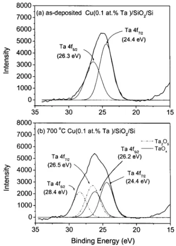
corrected for the charging effect with reference to the adventitious carbon 1s peak at 284.6 eV. Figure 6 shows the XPS spectra of Ta 4f core levels for the as-deposited and 700°C annealed Cu(0.1 atom % Ta)/SiO2 interfaces. For the as-deposited Cu(0.1 atom % Ta)/SiO2interface, the Ta 4f doublet has peaks lo-cated at 24.4 (4f7/2) and 26.3 eV (4f5/2). Because the position of this Ta 4f doublet is 2 eV lower than that of Ta2O5doublet共Ta 4f7/2of Ta2O5⫽ 26.4 eV21兲 but is 2.5 eV higher then that of the metallic Ta 4f doublet共Ta 4f7/2of metallic Ta⫽ 21.9 eV15兲, the bonding state of Ta here should be corresponding to that of incompletely oxidized Ta共referred to TaOx).22After annealing at 700°C, the Ta signal is composed of two sets of Ta 4f doublets. The doublet at the higher energy side shows binding energy (Ta 4f7/2⫽ 26.5 eV) close to the chemical state of Ta2O5, while the doublet at the lower energy side is still associated with TaOx. However, the integrated intensity of the overall Ta 4f signal at the 700°C annealed Cu(0.1 atom % Ta)/SiO2 interface does not differ significantly from that of as-deposited sample.
Figure 7 exhibits the XPS spectra of Ta 4f core levels ob-tained from the as-deposited and 700°C annealed Cu(2.3 atom % Ta)/SiO2interfaces. Both TaOx(Ta 4f7/2⫽ 24 eV) and Ta2O5 bonding (Ta 4f7/2⫽ 26.2 eV) were observed at the Cu(2.3 atom % Ta)/SiO2 interface, before and after annealing at 700°C. The intensity of Ta 4f signal corresponding to the chemical state of Ta2O5was much greater than that of TaOx. In the Cu共0.1 atom % Ta兲 system, the intensity of Ta2O5 bonding was not ob-served in the as-deposited sample and it was not stronger than that of TaOx bonding even after annealing at 700°C共Fig. 6兲. Formation of Ta2O5 in Cu共Ta兲 共Ta-rich兲 system can be understood from the thermodynamics of chemical reaction.23For oxidation of metal to its
stable oxide, the Gibbs free energy of reaction,⌬G, is Ta⫹ 5
4O2→ 1
2Ta2O5 ⌬G ⫽ ⌬G
0⫹ RT ln Q
where ⌬G0 is the standard Gibbs free energy change and Q ⫽ aTa2O5
1/2
/aTaaO2 5/4
is the activity quotient. Activity of oxygen is equal to its partial pressure共assuming ideal behavior of oxygen兲 and it should be a constant for a given experimental condition共at constant temperature兲. ⌬G0is a negative number for the formation of Ta
2O5 and it is a function of temperature only.24 However, since pO2(⫽aO2) is rather small 共the samples where in vacuum during deposition and annealing兲 and aTa⬍ 1 (aTa⬇ XTa for dilute Ta in Cu alloy兲, the RT ln Q term can be very large and the ⌬G value may become positive. Once the aTa is larger 共i.e., greater Ta content in the alloy兲, the RT ln Q term will be smaller and the ⌬G will be negative. Therefore, we observed Ta2O5 at the Cu(2.3 atom % Ta)/SiO2 system, but not in the Cu(0.1 atom % Ta)/SiO2system.
In Fig. 7b, an addition set of doublet at the low energy side (Ta 4f7/2⫽ 22 eV,Ta 4f5/2⫽ 23.8 eV) may be pertained to metallic Ta共or Ta with very few oxygen neighbors兲. In addition, the inte-grated Ta signal intensity of the 700°C annealed Cu(2.3 atom % Ta)/SiO2 interface was much greater than that of the as-deposited Cu(2.3 atom % Ta)/SiO2interface and that of the 700°C annealed Cu(0.1 atom % Ta)/SiO2interface. This result im-plies that the Ta2O5 共or TaOx) thickness of 700°C annealed Cu(2.3 atom % Ta)/SiO2 sample was thicker than that of 700°C annealed Cu(0.1 atom % Ta)/SiO2sample. Therefore, the Cu-SiO2 interdiffusion shall be more effectively retarded in the
Figure 6. XPS spectra of Ta 4f core levels obtained from the SiO2surface of the Cu(0.1 atom% Ta)/SiO2/具Si典system after etching the metal over layer. 共a兲 As-deposited and 共b兲 700°C annealed.
Figure 7. XPS spectra of Ta 4f core levels obtained from the SiO2surface of the Cu(2.3 atom% Ta)/SiO2/具Si典system after etching the metal over layer. 共a兲 As-deposited and 共b兲 700°C annealed.
Cu(2.3 atom % Ta)/SiO2sample. To prove this proposition, interfa-cial diffusion characteristics of the samples were examined as follows.
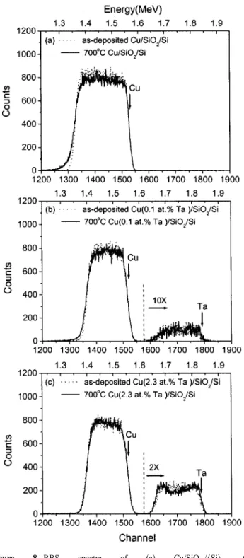
Figure 8 presents the RBS spectra of Cu/SiO2/具Si典, Cu(0.1 atom % Ta)/SiO2/具Si典, and Cu(2.3 atom % Ta)/SiO2/具Si典 samples, before and after annealing at 700°C. Comparing to their as-deposited spectra, the Cu profiles in the 700°C annealed spectra of Cu/SiO2/具Si典 and Cu(0.1 atom % Ta)/SiO2/具Si典 exhibit a drooping tail at the lower-energy Cu edge共⬃channel 1300 and be-low兲. It implies that copper had diffused into SiO2after annealing at
Ta signals are observed in both as-deposited and 700°C annealed spectra of the Cu共0.1 atom % Ta兲 and Cu共2.3 atom % Ta兲 systems 共Fig. 8b and c兲. Because the Ta profiles span over the Cu layers in the annealed samples, considerable amount of Ta additives still re-main within the Cu layers after annealing. However, because XRD analysis indicates that the lattice spacing of the annealed Cu共Ta兲 film restored to that of the pure Cu共see Fig. 2兲, the Ta atoms should mostly segregate to the Cu grain boundaries upon annealing. The Ta atoms decorate on the grain boundaries will inhibit the Cu grain growth and consequently preserve the smooth surface morphology 共see Fig. 4c and f兲. However, there may still exist residual Ta atoms within the Cu lattices. Both residual Ta atoms and small Cu grain size can explain why the resistivity of annealed Cu共2.3 atom % Ta兲 films is still greater than that of annealed pure Cu films. When we look closely, the Ta profile of the 700°C annealed Cu共2.3 atom % Ta兲 sample has slightly higher counts on the free surface and at Cu(2.3 atom % Ta)/SiO2 interface. It indicates that a part of Ta atoms segregated to the free surface and Cu(2.3 atom % Ta)/SiO2 interface. This observation is consistent with the enlargement of Ta XPS intensity at the Cu(2.3 atom % Ta)/SiO2 interface after an-nealing at 700°C共Fig. 7b兲.
As a summary, although the resistivity of annealed Cu共2.3 atom % Ta兲 film is evidently larger than that of annealed pure Cu film, Cu共2.3 atom % Ta兲 system exhibits superior characteristics of mor-phology and Cu/SiO2interdiffusion than other two systems. These advantages may be critical for reducing the thickness of diffusion barrier, which is another factor on the determination of the overall resistivity. In the future study, the connection between the Cu共Ta兲 films and the optimal thickness of diffusion barrier (TaNx) should be investigated. Therefore, Cu(Ta)/TaNxmay possess smooth morphol-ogy, low degree of Cu diffusion, and low-enough sheet resistance for microelectronic application.
Conclusion
In this study, we have investigated the influences of Ta additives in Cu on the microstructure, interface reaction, and diffusion of Cu/SiO2upon vacuum annealing. Since Cu-Ta is an immiscible bi-nary system, Ta additives in Cu lattices segregated spontaneously upon annealing. An additional Ta2O5共or TaOx) layer was observed at the Cu(Ta)/SiO2 interface after annealing. This layer acts as a barrier to prevent the diffusion of Cu into SiO2. The barrier effect is particularly evident for the Cu共2.3 atom % Ta兲 system. In this sys-tem, RBS analysis does not observe diffusion of Cu into SiO2even upon annealing at 700°C. In addition, the Cu共2.3 atom % Ta兲 films exhibit very low degree of grain growth and smooth surface after annealing upto 800°C, possibly due to the segregation of Ta addi-tives on the grain boundaries. The morphological characteristics im-ply the inhibition of agglomeration and migration of Cu atoms. However, the resistivity of annealed Cu共2.3 atom % Ta兲 films is still too high. In combination with a diffusion barrier of adequate
thick-Figure 8. RBS spectra of 共a兲 Cu/SiO2/具Si典, 共b兲
Cu(0.1 atom% Ta)/SiO2/具Si典, and 共c兲 Cu(2.3 atom% Ta)/SiO2/具Si典 samples, before and after annealing at 700°C. Surface scattering energies of Cu and Ta are indicated with arrows and the Ta profiles are magnified for clarity.
ness, Cu共Ta兲 alloy will be an advantageous metallization material for ULSI applications owing to its exceptional morphology and low degree of Cu diffusion.
Acknowledgment
The authors gratefully acknowledge the financial support from the National Science Council of Taiwan, R.O.C.共grant no. NSC-89-2216-E-006-037兲.
National Cheng Kung University assisted in meeting the publication costs of this article.
References
1. S. P. Murarka, Mater. Sci. Eng., 19, 87共1997兲. 2. E. R. Weber, Appl. Phys. A: Solids Surf., 30, 1共1983兲.
3. J. D. McBrayer, R. M. Swanson, and T. W. Sigmon, J. Electrochem. Soc., 133, 1242共1986兲.
4. S. W. Russell, S. A. Rafalski, R. L. Spreitzer, J. Li, M. Moinpour, F. Moghadam, and T. L. Alford, Thin Solid Films, 262, 154共1995兲.
5. J. Li, J. W. Mayer, Y. Shacham-Diamand, and E. G. Colgan, Appl. Phys. Lett., 60, 2983共1992兲.
6. D. Adams, T. L. Alford, S. A. Rafalski, M. J. Rack, S. W. Russell, M. J. Kim, and J. W. Mayer, Mater. Chem. Phys., 43, 145共1996兲.
7. K. Hoshion, H. Yagi, and H. Tsuchikawa, in Proceedings of the 7th International VLSI Multilevel Interconnection Conference, IEEE, p. 357共1990兲.
8. C. J. Liu and J. S. Chen, Appl. Phys. Lett., 80, 2678共2002兲.
9. C. J. Liu, J. S. Jeng, and J. S. Chen, J. Vac. Sci. Technol. B, 20, 2361共2002兲. 10. K. Barmak, G. A. Lucadamo, C. Cabral, Jr., C. Lavoie, and J. M. E. Harper, J.
Appl. Phys., 87, 2204共2000兲.
11. M. H. Tsai, S. C. Sun, C. E. Tsai, S. H. Chuang, and H. T. Chiu, J. Appl. Phys., 79, 6932共1996兲.
12. M. T. Wang, Y. C. Lin, and M. C. Chen, J. Electrochem. Soc., 145, 2538共1998兲. 13. H. J. Lee, K. W. Kwon, C. Ryu, and R. Sinclair, Acta Metall., 47, 3965共1999兲. 14. H. Wang, M. J. Zaluzec, and J. M. Rigsbee, Metall. Mater. Trans. A, 28, 917
共1997兲.
15. J. F. Moulder, W. F. Stickle, P. E. Sobol, and K. D. Bomben, Handbook of X-Ray Photoelectron Spectroscopy, Physical Electronics, Inc., Eden Prairie, MN共1995兲. 16. J. P. Chu and T. N. Lin, J. Appl. Phys., 85, 6462共1999兲.
17. P. R. Subrmanian and D. E. Laughlin, Bull. Alloy Phase Diagrams, 10, 652共1989兲. 18. K. T. Miller, F. F. Lange, and D. B. Marshell, J. Mater. Res., 5, 151共1990兲. 19. B. D. Cullity and S. R. Stock, Elements of X-Ray Diffraction, 3rd ed., p. 170,
Prentice Hall, New Jersey共2001兲.
20. T. Nemoto and T. Nogami, in Proceedings of the 32nd Symposium on Reliability Physics, IEEE, p. 207共1994兲.
21. G. E. McGuire, G. K. Schweitzer, and T. A. Carlson, Inorg. Chem., 12, 2450 共1973兲.
22. S. Lecuyer, A. Quemerais, and G. Jezequel, Surf. Interface Anal., 18, 257共1992兲. 23. D. R. Gaskell, Introduction to the Thermodynamics of Materials, 3rd ed., Chap. 13,
Taylor & Francis, Washington, D.C.共1995兲.
24. I. Brain, Thermochemical Data of Pure Substances, 3rd ed., VCH, Weinheim 共1995兲.