at 150 °C
Chia-Wei Huanga)and Kwang-Lung Lin
Department of Materials Science and Engineering, National Cheng Kung University, Tainan 701, Taiwan, Republic of China
(Received 17 June 2004; accepted 27 August 2004)
The interfacial reactions of Sn–Zn based solder on Cu and Cu/Ni–P/Cu–plating substrates under aging at 150 °C were investigated in this study. The compositions of solders investigated were Sn–9Zn, Sn–8.55Zn–0.45Al, and Sn–8.55Zn–0.45Al–0.5Ag solders in weight percent. The experimental results indicated that the Cu substrate formed Cu5Zn8with the Sn–9Zn solder and Al–Cu–Zn compound with Al–containing solders. However, it was detected that Cu6Sn5formed at the Sn–9Zn/Cu interface and Cu5Zn8formed at the Al–containing solders/Cu interface after aging for 1000 h. When it contacted with the Cu/Ni–P/Au substrate, the Sn–9Zn solder formed Au–Zn
compound, and the Al–containing solders formed Al–Cu–Zn compound at the interface. After a long aging time, the intermetallic compounds existing between solders and the Cu/Ni–P/Au metallization layers almost did not grow. It was found that the interdiffusion between solders and Cu/Ni–P/Au was slower than that with Cu under aging. Furthermore, the addition of Ag to Sn–Zn solder resulted in the formation of AgZn3particles at the interface.
I. INTRODUCTION
Sn–Pb solders have been generally used for metal bonding in microelectronic assemblies because of low melting temperature, low cost, ease of handling, good ductility, workability, and excellent wettability on com-monly used substrates.1,2
However, legislative action in Europe will ban the use of lead-based solders in the near future. Therefore, the development of lead-free solders has become an important issue in the electronics pack-aging industry. A great number of research articles have been published on the subject of lead-free solders re-cently. Among the solders investigated, Sn–Zn solders are expected to be a potential alternative to eutectic Sn–Pb solder.
The eutectic Sn–9Zn solder has a melting temperature (198 °C) relatively close to that of eutectic Sn–Pb solder (183 °C).2,3 This will allow the industry to apply the present manufacturing line and electronic components without much modifications. Sn–Zn solders also have greater mechanical strength than the conventional Sn–Pb solders and cost less than other lead-free solders.2 Un-fortunately, Sn–Zn solders exhibit unsatisfactory wetta-bility as zinc is easily oxidized leading to the formation
of an oxide layer.2 Thus, a protective atmosphere or an aggressive flux is needed during the manufacturing of electronic interconnections when using Sn–Zn solders. From the application point of view, an enhancement in wettability and oxidation resistance of Sn–Zn solders is necessary. Sebaoun and Lin observed an improvement in the oxidation resistance on addition of Al to the Sn–Zn solder.4,5It has been reported that a small addition of Ag is also able to enhance the wettability of Sn–Zn solders on Cu substrates.6
Recent studies7–11 have indicated that the interfacial reaction products, such as intermetallic compounds, be-tween substrates and solder alloys have a great effect on the mechanical properties and reliability of solder joints. It is due to the fact that the brittle nature of the inter-metallic compounds and the joining of two materials with dissimilar coefficient of thermal expansion cause degradation of interface integrity between substrates and solders. Especially in the avionics and automotive appli-cations, the reliability of solder joints heavily depends on the interfacial structure because the solder joint is sub-jected to thermal cycles and high temperature circum-stances up to 150 °C. A previous paper11 has indicated that the interfacial morphology change of Sn–9Zn/Cu joint causes serious degradation of joint strength under thermal aging at 150 °C. It has been reported that cracks can be initiated and can propagate along the interface between the intermetallic compound and solder under
a)
Address all correspondence to this author. e-mail: [email protected] DOI: 10.1557/JMR.2004.0458
thermal fatigue test. Hence, a deeper understanding of interfacial reaction between solder and substrate is re-quired for the design and systematic evaluation of a new lead-free solder alloy. This present study investigated the formation of intermetallic compounds and growth behav-ior of Sn–9Zn, Sn–8.55Zn–0.45Al, and Sn–8.55Zn– 0.45Al–0.5Ag solders on Cu and Cu/Ni–P/Au substrates under aging at 150 °C.
II. EXPERIMENTAL PROCEDURE
The lead-free solder alloys investigated in this study were prepared by melting eutectic Sn–3.5Ag solder, Zn–5Al, pure Zn, and pure Sn to achieve the desired compositions. The compositions of the resulting solders were Sn–9Zn, Sn–8.55Zn–0.45Al, and Sn–8.55Zn– 0.45Al–0.5Ag in weight percent. The Cu foils were used as the substrates. Some foils were plated with a 2–3m electroless Ni film (containing 6–8 wt% P) followed by a 0.1-m Au layer. The electroless nickel deposition was conducted in a pH 4.6 nickel sulfate solution at 82 °C for 20 min with sodium hypophosphite used as the reduc-tant.12The Au layer was deposited electrolessly in a gold potassium cyanide solution of pH 7 at 92 °C for 5 min with sodium hypophosphite as the reductant. The sub-strates were degreased in NaOH, deoxidized in nitric acid solution, and then dipped in the flux consisted of 2.5 g dimethylammonium chloride (DMAHCl) and 100 ml n-butyl alcohol before the testing began. Then the Cu and Cu/Ni–P/Au foil were dipped into the molten solder bath. The dipping time was 120 s, the dipping speed was 15 mm/s, and the dipping temperature was 250 °C. The soldered specimens were aged in an oven at 150 °C for 0, 500, and 1000 h. The interfaces between solders and substrates were investigated with scanning electron microscopy (SEM) and electron probe microanalysis (EPMA). The composition of the precipitates and phases between solders and substrates was analyzed with energy dispersive spectroscopy (EDS) and wavelength disper-sive spectrometer (WDS).
III. EXPERIMENTAL RESULTS
A. Interfacial reactions between the Sn–9Zn solder and the Cu substrate under aging
Figure 1 shows the SEM photographs of the interfaces between the Sn–9Zn solder and the Cu substrate under aging at 150 °C for 0, 500, and 1000 h. Figure 1(a) shows that two compound layers formed at the interface before aging. The 3-m-thick inner compound layer was con-firmed to be␥–Cu5Zn8phase by EDS analysis. The com-position of the 1-m-thick outer compound layer was identified to be Cu, Zn, and a small amount of Sn (about 17Cu–80Zn–3Sn in atomic percent). This chemi-cal composition shows that the layer is–CuZn5phase.
Figures 1(b) and 1(c) show the Sn–9Zn/Cu interfaces after aging for 500 and 1000 h, respectively. It was found that the thickness of Cu5Zn8 compound increased when aging time increased, but no more CuZn5compound was identified. The –CuZn5 compound seemed to coalesce and transform to Cu5Zn8 compound upon aging. The Cu5Zn8compound layer grew to about 10-m-thick after aging for 1000 h.
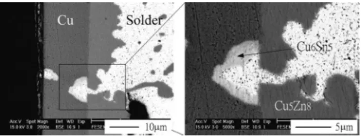
In addition to the compound layer formed at the inter-face, it was found that the Cu5Zn8particles also formed within the Sn–9Zn solder, and the fraction of the Cu5Zn8 particles increased with increasing aging time. It was also found that the fraction of the needlelike Zn–rich phase decreased as aging time increased. The Zn–rich phase almost disappeared around the interface after aging for 1000 h as seen in Fig. 1(c). Aside from the planar ␥–Cu5Zn8 compound, a new phase was observed at the interface under aging for 1000 h as shown in Fig. 2. The result of EDS analysis indicated that this new phase com-posed of Cu and Sn (about 58Cu–42Sn in atomic per-cent). This chemical composition renders the compound to be–Cu6Sn5. In Fig. 2, the Cu5Zn8compound seemed to be disrupted locally at the interface, and the Cu6Sn5 compound formed close to the Cu substrate. The phe-nomenon was not observed at the interface for aging time less than 500 h.
FIG. 1. SEM photographs of the interfaces between Sn–9Zn solder and Cu substrate under aging at 150 °C for (a) 0 h, (b) 500 h, and (c) 1000 h.
B. Interfacial reactions between the Sn–Zn–Al, Sn–Zn–Al–Ag solders and the Cu substrate under aging
Figure 3 shows the EPMA elemental mapping analysis of the interfaces of the Cu/Sn–Zn–Al and Cu/Sn–Zn– Al–Ag specimens before aging. It was found that the interfacial morphologies of these two specimens are quite different from that of the Cu/Sn–9Zn specimen.
The continuous interfacial layer formed between Cu and the solders appear to be only about 0.5 m thick and consist of Al, Zn, and Cu. This result shows that the Al participated in the interfacial reaction but suppressed the growth of the interfacial compound layer. It has been reported previously that the interfacial layer is the Al4.2Cu3.2Zn0.7 compound.
13,14
Aside from the Al–Cu– Zn compound, a spherical and discontinuous Ag–Zn compound formed between the Al–Cu–Zn compound and the Sn–Zn–Al–Ag solder. The result of EDS analysis indicated that this compound is the AgZn3.
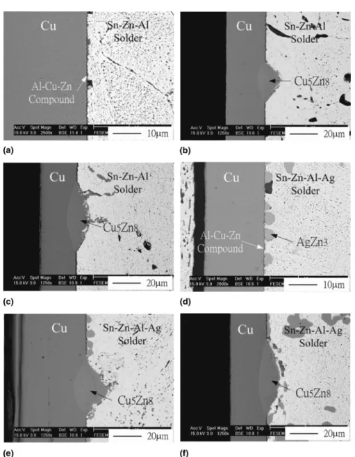
Figure 4 shows the SEM photographs of the interfaces of the Cu/Sn–Zn–Al and Cu/Sn–Zn–Al–Ag specimens before and after aging. A thin layer of an Al–Cu–Zn compound and the spherical AgZn3compound were also found at the interface between the Al–Cu–Zn compound and the solder before aging. However, a Cu–Zn com-pounds was found at the interface after aging for 500 h as shown in Figs. 4(b), 4(c), 4(e), and 4(f). The Cu–Zn FIG. 2. SEM photographs of the interfaces between Sn–9Zn solder
and Cu substrate under aging at 150 °C for 1000 h.
FIG. 3. EPMA elemental mapping analysis of the solder–Cu interfaces before aging, (a) Cu/Sn–8.55Zn–0.45Al and (b) Cu/Sn–8.55Zn–0.45Al– 0.5Ag.
compound was identified to be the␥–Cu5Zn8compound by EDS analysis. This compound grew up to about 10m thick after aging for 1000 h. It was found that the thickness of Al–Cu–Zn compound (1m) did not grow much after aging. The thickness of this layer was much thinner than that of the Cu5Zn8compound formed at the Sn–Zn solder/Cu interface [Fig. 1(c)] after aging for 1000 h. C. Interfacial reactions between the solders and the Cu/Ni–P/Au substrate under aging
Figure 5 shows the EPMA elemental mapping analysis of the interfaces between the solders and the Cu/Ni–P/Au substrate before aging. Figure 5(a) shows that a thin layer of an Au–Zn compound formed at the Sn–Zn solder and Cu/Ni–P/Au interface. The Au–Zn compound, less than
0.5 m thick, was thinner than the Cu5Zn8 compound formed between the Sn–9Zn solder and the Cu substrate [Fig. 1(a)]. It was found that the interfacial reaction be-tween the Sn–9Zn solder and the Cu/Ni–P/Au was slower and different from that with the Cu substrate. The interfacial reaction between the Sn–Zn–Al and the Sn– Zn–Al–Ag solders and the Cu/Ni–P/Au substrates also gave rise to a thin compound layer containing Au, Al, and Zn, as seen in Figs. 5(b) and 5(c). The thickness of the Al–Au–Zn layer is also less than 0.5m. This result shows that the Al not only participates in the interfacial reaction between the solders and the Cu but also partici-pates in the region with the Cu/Ni–P/Au substrate. A spherical compound, AgZn3, was detected at the inter-face between the Sn–Zn–Al–Ag solder and the layer that contains Al, Au, and Zn. A previous study14
confirmed FIG. 4. SEM photographs of the Cu/Sn–8.55Zn–0.45Al after aging for (a) 0 h, (b) 500 h, (c) 1000 h, and the Cu/Sn–8.55Zn–0.45Al–0.5Ag after aging for (d) 0 h, (e) 500 h, and (f) 1000 h.
that the compounds consisting of Al, Au, and Zn are the AuZn3at the Sn–Zn solder–Cu/Ni-P/Au interface and the Al2(Au, Zn) between the Sn–Zn–Al, Sn–Zn–Al–Ag sol-ders, and the Cu/Ni–P/Au substrate.
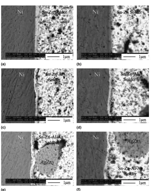
The SEM images of the interfaces between solders and the Cu/Ni–P/Au substrate before and after aging are shown in Fig. 6. These results show that the interfacial morphology almost did not have any variation during FIG. 5. EPMA element mapping photographs of the solder–Cu/Ni–P/Au interfaces before aging, (a) Sn–9Zn, (b) Sn–8.55Zn–0.45Al, and (c) Sn–8.55Zn–0.45Al–0.5Ag.
aging. Figure 7 shows the SEM photographs and the line-scanning analysis at the interface between the sol-ders and the Cu/Ni–P/Au substrate after aging for 1000 h. It further shows that the interfacial layers contain the Au–Zn and Al–Au–Zn compounds. This result implies that the interfacial compounds formed between the sol-ders and the substrate did not grow and no new com-pound formed during aging.
IV. DISCUSSION
A. Interfacial evolutions between Sn–9Zn solder and Cu substrate under aging
It has been reported that Cu5Zn8 and CuZn5 com-pounds formed at the interface between the Sn–Zn solder and the Cu substrate.15
In this study, Cu5Zn8and CuZn5 compounds, formed between Sn–9Zn solder and Cu with
a thickness of about 3m and 1 m, were also detected after dipping for 120 s as seen in Fig. 1(a). However, only the Cu5Zn8compound was detected at the interface under aging. The–CuZn5 compound seemed to trans-form to␥–Cu5Zn8compound upon aging. The standard Gibbs free energy of formation at 773 K for –CuZn5 compound is −1700 to −2100 cal/g atm and that of ␥–Cu5Zn8 compound is −2700 to −3100 cal/g atm.
16 Thus, the CuZn5 compound will tend to transform to Cu5Zn8compound thermodynamically. The thickness of the Cu5Zn8 compound increases as the aging time in-creases. It was also found that the isolated Cu5Zn8 par-ticles formed in the solder, while the Zn-rich phase dis-appeared under aging as seen in Figs. 1(b) and 1(c). This implies that Cu atoms moved through the planar Cu5Zn8 compound and reacted with Zn atoms to form the iso-lated Cu5Zn8 particles in the solder during aging. This
FIG. 6. SEM photographs of the solder–Cu/Ni–P/Au interfaces; Sn–9Zn (a) as soldered, (b) aged 1000 h; Sn–8.55Zn–0.45Al (c) as soldered and (d) aged 1000 h; Sn–8.55Zn–0.45Al (e) as soldered and (f) aged 1000 h.
behavior can be ascribed to the fact that the magnitude of diffusivity of Cu in Sn matrix is larger than that of Zn. This may cause the lack of Zn around the interface in the solder under aging. Therefore, the Cu atom kept on dif-fusing into the solder as aging time increased. The Cu6Sn5compound was formed (Fig. 2) between the Sn– 9Zn solder and the Cu substrate after aging for 1000 h due to the absent of Zn atom around the interface. Pre-vious studies11
also indicated that Cu6Sn5compound is observed at the interface between the Sn–Zn solder and the Cu substrate, which results in serious degradation of joint strength after aging at 150 °C.
B. Interfacial evolutions between Sn–Zn–Al and Sn–Zn–Al–Ag solders and Cu substrate
under aging
In Fig. 3, it was found that an Al–Cu–Zn compound, about 0.5m thick, formed at the interface between the solders and the Cu substrate after dipping. Previous stud-ies13,14have indicated that the Al4.2Cu3.2Zn0.7compound was formed at the interface as the 0.45 wt% Al was added to the solders. It is known that Al is an active element. Thus, the Al may easily tend to move to inter-face and react with Cu and Zn and form the compound. The Al–Cu–Zn compound was relatively thinner than that of the Cu5Zn8compound formed at the Sn–9Zn/Cu
interface as shown in Fig. 1. This means that the Al not only participates in the interfacial reaction but also im-pedes the interdiffusion between solders and Cu during dipping. It was also found that the Al–Cu–Zn compound almost did not grow during aging at 150 °C as seen in Fig. 4. The thickness of that was still less than 1m after aging for 1000 h. However, the Cu5Zn8 compound was detected at the interface after aging for more than 500 h. The formation of the Cu5Zn8may be due to the fact that the Al–Cu–Zn compound disrupted locally under aging, and then the Zn atoms in the solder can directly react with the Cu substrate to form the Cu5Zn8 compound. Besides the Al–Cu–Zn and Cu5Zn8 compounds, any Cu–Sn compounds were not detected at the interface be-tween solders and Cu after aging for 1000 h. It has been reported2,7,10 that the Cu substrate in contact with Sn–containing solders, like Sn–Pb, Sn–Ag, Sn–Ag–Cu, etc., will form Cu–Sn compound. In Fig. 2, it was also found that the Cu6Sn5 compound forms at the Sn–9Zn/Cu interface after aging for 1000 h. Neverthe-less, the Cu–Sn compound was not detected at the inter-face between the 0.45 wt% Al-containing solders and Cu even under aging for 1000 h. Thus, this implies that the addition of Al to Sn–Zn solder can inhibit the inter-diffusion between Sn and Cu to form compound under aging at 150 °C.
FIG. 7. SEM photographs and the line-scanning analysis of the solder–Cu interfaces after aging for 1000 h, (a) Sn–9Zn, (b) Sn–8.55Zn–0.45Al, and (c) Sn–8.55Zn–0.45Al–0.5Ag.
In addition to the Al–Cu–Zn compound, the spherical AgZn3compound was detected at the interface between the Sn–Zn–Al–Ag solders and the continuous Al–Cu–Zn compound as seen in Figs. 3 and 4. It is known that the Ag–Zn compound forms in the bulk solder as Ag is added to the Sn–Zn based solders.17–21
In this study, it was also found that the AgZn3compound formed at the interface, while the quantity of that decreased with in-crease of the cooling rate of solidification. Thus, it is inferred that the formation of AgZn3compound was en-hanced by heterogeneous nucleation at the interface dur-ing solidification. Furthermore, it was also found that the AgZn3particles almost did not grow under aging. C. Interfacial evolutions between Sn–Zn based solders and Cu/Ni–P/Au substrate under aging
Cu/Ni–P/Au substrates are commonly utilized for met-allization in the ball grid array (BGA) package. It is known that Au dissolves into the solder very rapidly, and that Ni3Sn4and Ni3P are formed at the interface during soldering with Sn–Pb solder.7,10However, the interfacial reactions of Sn–Zn-based solders with Cu/Ni–P/Au were found to be different from that of the Sn–Pb solders. A thin layer of Au–Zn or Al–Au–Zn compound formed at the solder–Cu/Ni–P/Au interface. Au did not dissolve into the solders. Instead, Au formed an intermetallic compound at the interface because Au can easily react with Al and Zn. The intermetallic compounds formed between the Sn–Zn based solders, and the Cu/Ni–P/Au substrate were thinner and smoother than that of Sn–Pb solders. After aging for 1000 h, it was found that the interfacial morphology between solder and Cu/Ni–P/Au almost did not change. Presence of compounds, like Ni3Sn4, was not seen at the solder–Cu/Ni–P/Au interface during aging. Recent studies8,22 indicated that the pull strength of the Sn–Zn solder on Ni–P/Au substrate was better than that of the Sn–Pb, Sn–Ag, and Sn–Ag–Cu solders. This is due to the fact that the thickness of the intermetallic compound between the Sn–Zn solder and Ni–P/Au substrate is thinner than that of the other sol-ders, and no Ni3P compound can be found at the Sn–Zn/ Au/Ni–P interface by SEM and TEM analysis. In the present study, a similar interfacial morphology was also found at the interface between Sn–Zn based solders and Cu/Ni–P/Au substrate. Hence, the Ni3P compound is not expected to be observed at the interface.
V. CONCLUSION
The formation of the intermetallic compounds be-tween Sn–Zn-based solders and Cu and Cu/Ni–P/Au sub-strates under aging at 150 °C was investigated. It was found that the Cu5Zn8compound formed at the Sn–9Zn/ Cu interface and in the Sn–9Zn solder during aging, and the Cu6Sn5compound formed closing to the Cu substrate
after aging for 1000 h because of the lack of Zn around the interface. The Al–Cu–Zn and Cu5Zn8 compounds were detected at the interface between the Al-containing solders and Cu substrate under aging, while the Cu6Sn5 compound can not be found even after aging for 1000 h. The Sn–9Zn solder and the Al-containing solders with Cu/Ni–P/Au substrate formed the Au–Zn and Al–Au–Zn compounds. It was found that the interfacial morpholo-gies between solders and Cu/Ni–P/Au almost did not change during aging. Ag-containing solder formed the AgZn3 particles that attach to the Al-containing com-pound at the interface. The interfacial reactions between Sn–Zn-based solders and Cu/Ni–P/Au substrate were slower than that with the Cu substrate under aging at 150 °C.
ACKNOWLEDGMENTS
Financial support of this work from National Science Council of Republic of China under NSC 92-2216-E-006-031 and NSC 92-2216-E-006-038 is gratefully acknowledged.
REFERENCES
1. S. Jin: Developing lead-free solders: A challenge and opportunity.
JOM 45, 13 (1993).
2. M. Abtew and G. Selvaduray: Lead-free solders in microelectron-ics. Mater. Sci. Eng. R 27, 95 (2000).
3. T.B. Massalski: Binary Alloy Phase Diagrams, 2nd ed. (ASM, New York, NY, 1987), pp. 1848, 2086.
4. A. Sebaoun, D. Vincent, and D. Treheus: Al–Zn–Sn phase dia-gram-isothermal diffusion in ternary system. Mater. Sci. Technol. 3,241 (1987).
5. K.L. Lin and T.P. Liu: High temperature oxidation of a Sn–Zn–Al solder. Oxid. Met. 50, 255 (1998).
6. T. Takemoto and T. Funaki: Role of electrode difference between lead-free solder and copper base metal in wetting. Mater. Trans.
JIM 43, 1784 (2002).
7. K. Zeng and K.N. Tu: Six cases of reliability study of Pb-free solder joints in electronic packaging technology. Mater. Sci. Eng.
R 38, 55 (2002).
8. M. Nishiura, A. Nakayama, S. Sakatani, Y. Kohara, K. Uenishi, and K.F. Kobayashi: Mechanical strength and microstructure of BGA joints using lead-free solders. Mater. Trans. JIM 43, 1802 (2002).
9. C.B. Lee, S.B. Jung, Y.E. Shin, and C.C. Shur: Effect of isother-mal aging on ball shear strength in BGA joints with Sn– 3.5Ag–0.75Cu solder. Mater. Trans. JIM 43, 1858 (2002). 10. K.N. Tu and K. Zeng: Tin-lead (SnPb) solder reaction in flip chip
technology. Mater. Sci. Eng. R 34, 1 (2001).
11. K. Suganuma: Heat resistance of Sn–9Zn solder/Cu interface with or without coating. J. Mater. Res. 15, 884 (2000).
12. K.L. Lin and C.W. Huang: Effect of thiourea and lead acetate on the deposition of electroless nickel. Mater. Chem. Phys. 76, 204 (2002).
13. K.L. Lin and H.M. Hsu: Sn–Zn–Al Pb-free solder—An inherent barrier solder for Cu content. J. Electron. Mater. 30, 1068 (2001).
14. C.W. Huang and K.L. Lin: Wetting properties of and interfacial reactions in lead-free Sn–Zn based solders on Cu and Cu plated with an electroless Ni-P/Au layer. Mater. Trans. JIM 45, 1 (2004). 15. H.M. Lee, S.W. Yoon, and B.J. Lee: Thermodynamic prediction of interface phases at Cu/solder joints. J. Electron. Mater. 27, 1161 (1998).
16. R. Hultgren: Selected Values of Thermodynamic Properties of
Metals and Alloys (Wiley, New York, NY, 1963), p. 712.
17. C.W. Huang and K.L. Lin: Microstructures and mechanical prop-erties of Sn–8.55Zn–0.45Al–XAg solders. J. Mater. Res. 18, 1528 (2003).
18. J.M. Song and K.L. Lin: Behavior of intermetallics in liquid Sn– Zn–Ag solder alloys. J. Mater. Res. 18, 2060 (2003).
19. M. McCormack, S. Jin, G.W. Kammlott, and H.S. Chen: New Pb-free solder alloy with superior mechanical properties. Appl. Phys.
Lett. 63, 15 (1993).
20. M. McCormack and S. Jin: Improved mechanical properties in new, Pb-free solder alloys. J. Electron. Mater. 23, 715 (1994). 21. M. McCormack, G.W. Kammlott, H.S. Chen, and S. Jin: New
lead-free, Sn–Ag–Zn–Cu solder alloy with improved mechanical properties. Appl. Phys. Lett. 65, 1233 (1994).
22. Y. Chonan, T. Komiyama, J. Onuki, R. Urao, T. Kimura, and T. Nagano: Influence of P content in electroless plated Ni-P alloy film on interfacial structures and strength between Sn–Zn solder and plated Au/Ni–P alloy film. Mater. Trans. JIM 43, 1887 (2002).