of self-catalyzed vapor-liquid-solid 共VLS兲 technology. It was found that tips of the ZnO nanowires are hexagonal. It was also found that average length of the ZnO nanowires increased while the average tip diameter of the ZnO nanowires decreased as the growth temperature increased.
Furthermore, it was found that the ZnO nanowires grown at 500 ° C were “tube-shaped” while the ZnO nanowires grown at 700 ° C were “cone-shaped.” Photoluminescence 共PL兲, x-ray diffraction 共XRD兲, and energy depersive x-ray 共EDX兲 results all indicate that the quality of our ZnO nanowires is good. © 2005 American Vacuum Society. 关DOI: 10.1116/1.2101600兴
I. INTRODUCTION
In recent years, one-dimensional 共1D兲 nanostructures, such as nanotubes,
1nanowires,
2nanobelts,
3nanorods,
4nanocables,
5and nanoribbons
6have stimulated great interest for scientific research and development due to their impor- tance in fundamental physics. The 1D nanostructures are also potentially useful in both nanoscale electronic and optoelec- tronic devices. Although many studies have been performed on Si and III-V nanowire systems,
7–15only few reports on 1D oxide systems can be found in the literature. These 1D oxide systems include SnO
2,
16SiO
2,
17GeO
2,
18ZnO,
19–21in- dium tin oxide 共ITO兲,
22and Al
2O
3.
23Among them, ZnO is an n-type semiconductor with a large exciton binding energy of 60 meV and a wide band gap energy of 3.37 eV. ZnO emits short-wavelength light at room temperature, conducts trans- parently and is piezoelectric. Previously, Huang et al.
24re- ported the successful gas phase synthesis of ZnO nanowires on a patterned Au catalyst by vapor-liquid-solid 共VLS兲 reac- tion at high temperatures 共i.e., 900–925 °C兲. Geng et al.
25modified this VLS technology and successfully grew ZnO nanowires on the Si substrate.
Very recently, Tseng et al.
26developed a low-temperature VLS process and demonstrated the selective area growth of ZnO nanowires at 550 ° C. They also reported that crystal quality and diameter of the as-grown ZnO nanowires
27de- pend strongly on the amount of Zn powder and the oxygen flow rate.
28To realize a feasible device such as field emission display, we need to control crystal quality and diameter of the as-grown ZnO nanowires. Tseng et al.
26found that one
can increase the diameter of the ZnO nanowires either by increasing the amount of Zn powder or by increasing the oxygen flow rate. However, it is still difficult to grow well- aligned single crystal ZnO nanowires and even more difficult to control the tip size of the ZnO nanowires. In this study, we report the growth of high density vertical single crystal ZnO nanowires on ZnO : Ga/ Si
3N
4/ SiO
2/ Si templates by two- step oxygen injection method
28without catalysts. The optical properties and structural characteristics of the ZnO nano- wires will be reported. The growth mechanism will also be discussed.
II. EXPERIMENTS
The synthesis technique used in this study is a modified self-catalyzed VLS method based on the evaporation of a Zn
a兲Electronic mail: [email protected]
FIG. 1. FE-SEM image shows the ZnO nanowires were selectively grown on ZnO : Ga/ Si3N4/ SiO2/ Si templates.
metallic source with a 2-step gas flow control.
28The evapo- ration process was carried out in a quartz tube located in a horizontal tube furnace. The diameter and length of the quartz tube were 5.0 and 70 cm, respectively. Zinc metal powder with a purity of 99.9% purchased from Strem Chemicals was used as the zinc vapor source. Prior to the growth of ZnO nanowires, we first oxidized Si substrates by thermal oxidation to achieve 30-nm-thick SiO
2films, fol- lowed by plasma enhanced chemical vapor deposition 共PE- CVD兲 of 50-nm-thick Si
3N
4films on top of the SiO
2films.
We subsequently deposited 50-nm-thick Ga-doped ZnO films on top of the Si
3N
4films by rf sputtering. From x-ray dif-
fraction 共XRD兲 measurements, it was found that the sput- tered ZnO:Ga films were preferred to be oriented in the 共002兲 direction. Standard photolithography and wet etching were then performed to define the stripe patterns with a stripe width of 10 m on the templates. The spacing between the stripes was also 10 m. During wet etching, the ZnO : Ga/ Si
3N
4/ SiO
2/ Si templates were dipped in HCl 共2%兲 for 3 min to remove the exposed regions of the ZnO:Ga layers. We then placed the patterned ZnO : Ga/ Si
3N
4/ SiO
2/ Si templates together with zinc vapor source on an alumina boat, and inserted them into the quartz tube of fur- nace. Streams of argon and oxygen gases were then intro-
FIG. 2. Cross section FE-SEM micrographs of the results from the two-step oxygen injection method for deposition zinc oxide nanowires on the ZnO : Ga/ Si3N4/ SiO2/ Si substrate with various growth temperatures of共a兲 500 °C, 共b兲 550 °C, 共c兲 600 °C, 共d兲 650 °C, and 共e兲 700 °C. The insets at the top left corner shows the same sample top view images.
duced into the furnace. The first step was to lead an argon flow of 54 sccm into the reaction system as the experiment began. When the furnace temperature reached 420 ° C, an oxygen flow of 0 – 3 sccm was added into the argon flow as the second step, until the end of experiment. It should be noted that oxygen was the only oxidizer during the synthesis.
Thus, properties of the deposited ZnO nanowires should de- pend strongly on oxygen flow rate and the reaction time. We have varied the growth conditions and found that the optimal growth condition was to keep oxygen and argon flow rates at 0.8 and 54.5 sccm, respectively. We then grew the ZnO nanowires under such a condition with various growth temperatures.
It should be noted that we carefully controlled the posi- tions of the patterned ZnO : Ga/ Si
3N
4/ SiO
2/ Si template, zinc vapor source, and alumina boat so that they were located at the same horizontal level and were heated at the same tem- perature. We also kept the distance between zinc vapor source and patterned ZnO : Ga/ Si
3N
4/ SiO
2/ Si template at 20 mm with the zinc vapor source placed at the upstream side. A mechanical pump was then used to evacuate the sys- tem and a programmable temperature controller was used to preciously control the furnace temperature with an accuracy of ±1 ° C. During the growth of ZnO nanowires, the pressure inside the quartz tube, growth temperature and growth time were kept at 10 Torr and 30 min, respectively. A Philips
PW3710 x-ray diffractometer and a JEOL JEM-2100F trans- mission electron microscopy 共TEM兲, operated at 200 kV, were then used to characterize the crystallographic and struc- tural properties of the as-grown ZnO nanowires. Surface morphologies of the samples and size distribution of the nanowires were characterized by a LEO 1530 field emission scanning electron microscope 共FESEM兲, operated at 5 keV.
Photoluminescence 共PL兲 properties of these as-grown ZnO nanowires were also characterized by a Jobin Yvon- Spex fluorolog-3 spectrophotometer. A Xe lamp emitting at 254 nm was used as the excitation source during PL measurements.
III. RESULTS AND DISCUSSION
Figure 1 shows FESEM image of the ZnO nanowires grown at 550 ° C viewed with a 30° title angle. It can be seen clearly that high density vertical ZnO nanowires with uni- form diameter and uniform length were selectively grown on ZnO : Ga/ Si
3N
4/ SiO
2/ Si templates. It should be noted that ZnO nanowires can only be grown on the sputtered ZnO:Ga layer. In other words, no nanowires could be grown directly on the Si
3N
4layer where the sputtered ZnO:Ga layer was etched. The inset of Fig. 1 shows an enlarged image of this sample. It should be noted that we clearly observed the boundary of these ZnO nanowires while no disordered ZnO nanowires were found. Figures 2 共a兲–2共e兲 show FESEM im- ages of the ZnO nanowires grown at 500 ° C, 550 ° C, 600 ° C, 650 ° C, and 700 ° C, respectively. The insets of Figs. 2共a兲–2共c兲 show top view FESEM images of the ZnO nanowires grown at 500 ° C, 550 ° C, and 600 ° C, respec- tively. It can be seen that tips of the ZnO nanowires are hexagon, which is probably due to the wurtzite structure of ZnO single crystal. For the ZnO nanowires grown at 650 ° C and 700 ° C, it was found that tips of the nanowires all topple down. Thus, top view FESEM images of these two samples are not available. Although high density vertical ZnO nano- wires were observed in all these five samples, it was found that diameter and length of these nanowires were different.
FIG. 3. Size distribution of the zinc oxide nanowires deposited on ZnO : Ga/ Si3N4/ SiO2/ Si templates with various growth temperatures.
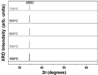
FIG. 4. XRD spectra共2= 25° – 65°兲 of the results from the deposition of zinc oxide nanowires on the ZnO : Ga/ Si3N4/ SiO2/ Si templates with various growth temperatures.
Figures 3 共a兲 and 3共b兲 show average length and average tip diameter, respectively, of the ZnO nanowires grown at dif- ferent temperatures. It can be seen clearly from Fig. 3共a兲 that the average length of the ZnO nanowires increased as the growth temperature increased. On the other hand, average tip diameter of the ZnO nanowires decreased as the growth tem- perature increased, as shown in Fig. 3共b兲. The root diameter of the ZnO nanowires grown at different temperatures is also shown in Fig. 3共a兲. Compare these root diameter values with the tip diameter values shown in Fig. 3共b兲. It was found that the root diameter 共i.e., 300–400 nm兲 and tip diameter 共i.e., around 400 nm兲 were about the same for the ZnO nanowires grown at 500° C. However, the ratio between root diameter and tip diameter increased as the growth temperature was increased. For the ZnO nanowires grown at 750 ° C, it was found that the root diameter 共i.e., 80–120 nm兲 was about five times larger than the tip diameter 共i.e., around 20 nm兲. In other words, the ZnO nanowires grown at 500 ° C were
“tube-shaped.” In contrast, the ZnO nanowires grown at 700 ° C were “cone-shaped.”
Figure 4 shows XRD spectra of these samples. It was found that only one strong ZnO 共002兲 XRD peak with small linewidth could be observed in these spectra. Such a result indicates that these ZnO nanowires were all well oriented with pure wurtzite structure. Figure 5 shows room tempera- ture PL spectra measured from the ZnO nanowires grown on ZnO : Ga/ Si
3N
4/ SiO
2/ Si with various growth temperatures.
It can be seen clearly that the all PL spectra exhibit a strong peak located at approximately 376 nm with long tails in the long wavelength region. The strong PL peak can be attrib- uted to the recombination of free excitons through the exciton-exciton collision process.
29Deep level emissions 共i.e., green-yellow bands兲 are also observed as the long tails shown in Fig. 5. It has been suggested that deep level emis- sions are related to the singly ionized oxygen vacancy in ZnO.
30Previously, it has been shown that defect related emissions are originated from radiative transitions between oxygen vacancy related shallow donors.
31Since the acceptor
level 共i.e., Zn vacancy兲 and the donor level are located at 2.5 and 0.05– 0.19 eV below the conduction band edge, respec- tively, the strong excitonic emission and the very weak deep level emission again indicate that quality of our ZnO nano- wires is good. Hu et al.
32proposed a model called self- catalyzed VLS growth. They suggested that Zn deposits va- porize in the form of liquid droplet. Liquidized zinc is involved in ZnO whisker growth. The Zn droplets then react with O
2to form ZnO. The melting temperature of ZnO is 1975 ° C, so the formation of ZnO on the Zn liquidized drop- lets proceeds by the VLS mechanism. Zn not only acts as a reactant but also provides an energetically favorable site for the absorption of O
2. Therefore, no transition metal need be added as a catalysts. Yao et al.
33reached a similar conclu- sion. However, they believed that Zn suboxides played the same role in the nucleation of ZnO nanowires as Zn, because both Zn and Zn suboxides have low melting temperatures 共approximately 419 °C for both Zn and ZnO
x, where x ⬍1兲.
FIG. 5. Room-temperature PL emission spectra of the results from the depo- sition of zinc oxide nanowires on ZnO : Ga/ Si3N4/ SiO2/ Si with various growth temperatures. These were excited atexc= 254 nm.
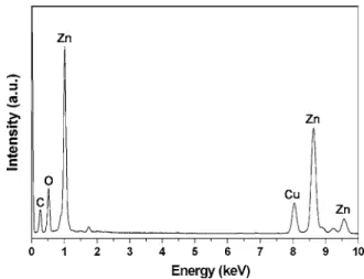
FIG. 6. EDX spectra of ZnO nanowires on the TEM copper grid.
FIG. 7. TEM image of the cross-sectional sample of the ZnO nanowires grown on the ZnO : Ga/ Si3N4/ SiO2/ Si templates.
The diameter of the ZnO nanowire was related to the Zn vapor pressure. The Zn vapor pressure was determined by the growth temperature. In the high temperature regime, ZnO nanowires show higher growth rate, meanwhile their length are longer and diameter are decreased.
Figure 6 shows energy dispersive x-ray 共EDX兲 spectrum of the ZnO nanowires grown at 550 ° C. It was found that the nanowires contain 58% zinc and 42% oxygen. The small amount of copper and carbon signals should originate from TEM copper grids and the carbon adhesion film. Figure 7 shows the cross-sectional HRTEM image of the ZnO nano- wires grown at 550 ° C. The brightness contrast observed in this image could be attributed to the diffraction patterns originated from various crystallographic planes. We thus be- lieve that the sputtered ZnO layer should have a grainy and columnar structure while the ZnO nanowires were grown along the columnar grains of the sputtered ZnO layer. Se- lected area electron diffraction 共SAED兲 image of the ZnO nanowires grown at 550 ° C is shown in the lower right por- tion of Fig. 8. Such a diffraction pattern also indicates that our ZnO nanowires are single crystal with wurtzite structure.
HRTEM image taken from the tip portion of the ZnO nano- wires grown at 550 ° C is shown in the upper left portion of Fig. 8. It can be seen clearly that the ZnO crystal lattices are well oriented with no observable defects in this region. The 0.52 nm lattice spacing observed from this figure is equiva- lent to two ZnO 共002兲 crystal planes. Such a result indicates our ZnO nanowires are structurally uniform and defect free.
It also suggests that the ZnO nanowires grown on ZnO : Ga/ Si
3N
4/ SiO
2/ Si templates are potentially useful in various optical and electrical applications.
J. Y. Li, X. L. Chen, H. Li, M. He, and Z. Y. Qiao, J. Cryst. Growth 233, 5共2001兲.
5J. Wu, S. Liu, C. Wu, K. Chen, and L. Chen, Appl. Phys. Lett. 81, 1312 共2002兲.
6B. D. Yao, Y. F. Chan, and N. Wang, Appl. Phys. Lett. 81, 757共2002兲.
7R. S. Wagner and W. C. Ellis, Appl. Phys. Lett. 4, 89共1964兲.
8E. I. Givargizov, J. Cryst. Growth 32, 20共1975兲.
9A. M. Morales and C. M. Lieber, Science 279, 208共1998兲.
10S. T. Lee, N. Wang, and C. S. Lee, Mater. Sci. Eng., A 286, 16共2000兲.
11C. C. Chen and C. C. Yeh, Adv. Mater.共Weinheim, Ger.兲 12, 738 共2000兲.
12J. Zhu and S. Fan, J. Mater. Res. 14, 1175共1999兲.
13M. Yazawa, M. Koguchi, A. Muto, M. Ozawa, and K. Hiruma, Appl.
Phys. Lett. 60, 2051共1992兲.
14X. F. Duan and C. M. Lieber, Adv. Mater.共Weinheim, Ger.兲 279, 208 共2000兲.
15Y. Homma, P. Finnie, T. Ogino, H. Noda, and T. Urisu, J. Appl. Phys. 86, 3083共1999兲.
16Z. R. Dai, Z. W. Pan, and Z. L. Wang, Adv. Funct. Mater. 13, 9共2003兲.
17Y. Q. Zhu, W. B. Hu, W. K. Hsu, M. Terrones, N. Grobert, J. P. Hare, H. W. Kroto, D. R. M. Walton, and H. Terrones, J. Mater. Chem. 9, 3173 共1999兲.
18Z. G. Bai, D. P. Yu, H. Z. Zhang, Y. Ding, X. Z. Gai, Q. L. Hang, G. C.
Xiong, and S. Q. Feng, Chem. Phys. Lett. 303, 311共1999兲.
19K. F. Nielsen, J. Cryst. Growth 3-4, 141共1968兲.
20J. Park, H. H. Choi, K. Siebein, and R. K. Singh, J. Cryst. Growth 258, 342共2003兲.
21J. Y. Li, X. L. Chen, H. Li, M. He, and Z. Y. Qiao, J. Cryst. Growth 233, 5共2001兲.
22H. Yumoto, T. Sako, Y. Gotoh, K. Nishiyama, and T. Kaneko, J. Cryst.
Growth 203, 136共1999兲.
23V. Valcarcel, A. Souto, and F. Guitian, Adv. Mater.共Weinheim, Ger.兲 10, 138共1998兲.
24M. H. Huang, Y. Wu, H. Feick, N. Tran, E. Weber, and P. Yang, Adv.
Mater.共Weinheim, Ger.兲 13, 113 共2000兲.
25C. Geng, Y. Jiang, Y. Yao, X. Meng, J. A. Zapien, C. S. Lee, Y. Lifshitz, and S. T. Lee, Adv. Funct. Mater. 14, 589共2004兲.
26Y. K. Tseng, I. N. Lin, K. S. Liu, T. S. Lin, and I. C. Chen, J. Mater. Res.
18, 718共2003兲.
27Y. K. Tseng, C. J. Huang, H. M. Cheng, I. N. Lin, K. S. Liu, and I. C.
Chen, Adv. Funct. Mater. 13, 812共2003兲.
28Y. K. Tseng, H. C. Hsu, W. F. Hsieh, K. S. Liu, and I. C. Chen, J. Mater.
Res. 18, 2837共2003兲.
29S. C. Lyu, Y. Zhang, H. Ruh, H.-J. Lee, H.-W. Shim, E.-K. Suh, and C. J.
Lee, Chem. Phys. Lett. 363, 134共2002兲.
30B. J. Jin, S. H. Bae, S. Y. Lee, and S. Im, Mater. Sci. Eng., B 71, 301 共2000兲.
31H. J. Egelhaaf and D. Oelkrug, J. Cryst. Growth 161, 190共1996兲.
32J. Q. Hu, Q. Li, N. B. Wong, C. S. Lee, and S. T. Lee, Chem. Mater. 14, 1216共2002兲.
33B. D. Yao, Y. F. Chan, and N. Wang, Appl. Phys. Lett. 81, 757共2002兲.
FIG. 8. High-resolution TEM image of an individual ZnO nanowire showing its 001 growth direction. The inset shows the corresponding selected-area electron diffraction pattern from the nanowires.