For the current subhalf-micrometer generation, any microscopic reaction at interfaces between interconnection layers will cause ex-cessive degradation of the integrated circuits. Consequently, diffusion barriers have become a critical component for improving the reliabil-ity of the metallization system. Interstitial compounds of refractory metals, including nitrides, borides, and carbides, have long been rec-ognized as materials for thin film diffusion barriers because of their high chemical stability, high atomic density, and good conductivity.1 Although titanium nitride (TiN) is currently the most popular diffu-sion barrier,2-4the columnar grain structure of sputtered TiN5is inad-equate since the grain boundaries offer fast paths for diffusion.
Titanium diboride (TiB2) has a high melting point (32258C) and a low resistivity (10,30 mV-cm, for bulk material).6The mass den-sity of TiB2is 4.52 g/cm3 7which can be converted to an atomic den-sity of 1.17 3 1023atom/cm3. This value is slightly higher than the atomic density of TiN (1.05 3 1023atom/cm3). Due to its high melt-ing point and high atomic density, TiB2 possess the fundamental characteristics of a good diffusion barrier. Shappirio et al.8reported that the contact stability of GaAs devices was significantly improved by applying a TiB2diffusion barrier. For the Si system, Choi et al.9 had examined the applicability of amorphous TiB2films, deposited by low pressure chemical vapor deposition (LPCVD) from TiCl4and B2H6, as diffusion barriers for Al and Cu metallizations. No signifi-cant reaction took place between Al and TiB2up to 6008C, and TiB2 did not react with Cu up to 7508C. It is also reported that sputtered TiB2from Ti and B targets served as a diffusion barrier against Cu penetration up to 6808C, when TiB2 is in an amorphous form.10 Interface mixing did not occur in a TiB2/Cu multilayered structure when irradiated with a 400 keV He21ion beam up to a dose of 123 1015ion/cm2.11It is shown in the paper that the Cu-TiB2interface shall be thermodynamically stable because the free energies of reac-tion for possible reacreac-tions between Cu and TiB2are all positive.11 Therefore, TiB2is a good candidate for a diffusion barrier for Cu metallization. In this work, TiB2films are synthesized by co-sput-tering from boron and TiB2targets. The reason for using both boron and TiB2targets is to obtain stoichiometric (or slightly boron-rich) TiB2films with low resistivity. The potential use of TiB2films as the diffusion barrier for Cu/<Si> (where <Si> represents the single-crys-talline Si substrate) metallization is investigated by characterizing the thermal reaction of Cu/TiB2/<Si> stacks annealed at 400-8008C.
Experimental
Unpatterned n-type Si(100) wafers of resistivity 7-10 V-cm were used as substrates in this study. The substrates were degreased in organic baths and chemically etched with dilute HF solution just prior
to loading into the deposition chamber. Thin films of TiB2were co-sputtered from a titanium diboride target with a dc power supply and a boron target with a rf power supply in an Ar ambient of 99.999% purity. The reason for using rf power for sputtering a boron target is because of the poor conductivity of the boron target. Both targets are 5 cm in diam and the target-to-substrate distance is about 10 cm. The substrate holder was neither heated nor cooled, but various dc sub-strate biases (0 to 2200 V) were applied to the holder. The base pres-sure of the deposition chamber was 3 3 1026Torr and the operation pressure was 7 mTorr. The thickness of the sputtered Ti-B films for material characterization was 100 nm. The Ti-B films were charac-terized using Auger electron spectroscopy (AES) for chemical com-positions, X-ray diffraction (XRD) with a glancing incident angle of 58 for crystal structures, and X-ray photoelectron spectroscopy (XPS) for chemical bonding states. The X-ray source for XPS is a mono-chromatized Mg Ka line (1253.6 eV). The film resistivity was calcu-lated from the sheet resistance measured by a four-point probe, and the film thickness measured by a Tencor a-step profilometer.
To test the thermal stability of the TiB2barriers, copper films of 180 nm thick were sputtered over the 60 nm thick TiB2layers. The samples were then annealed in a tube furnace at 400-8008C for 30 min in a flowing 80% Ar120% H2atmosphere. Hydrogen gas was employed to prevent the oxidation of copper during the heat-treatment. Surface morphology and phase formation for the samples after annealing were characterized by scanning electron microscopy (SEM) and glancing-angle XRD. Constituent elements at local re-gions of the samples were analyzed by both energy-dispersive analy-sis of X-rays (EDAX) and AES. The sheet reanaly-sistances of samples, before and after annealing, were measured with a four-point probe.
Results and Discussion
Material characteristics of co-sputtered TiB2thin
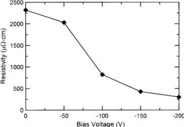
films.—Resis-tivity of the Ti-B films fabricated by sputtering from a hot-pressed TiB2target was as high as 2900 mV-cm. This value is far higher than the resistivity of bulk TiB2. Even when sputtering from both TiB2 and B targets, the composition and resistivity of the co-sputtered Ti-B films were still sensitive to deposition parameters such as the sput-tering power and the bias applied on the substrate. When the dc power on the TiB2target was 150 W and the rf power on the boron target was 150 W, the co-sputtered Ti-B films were 2300 mV-cm in resistivity. This is the lowest resistivity obtained without employing substrate bias. The film resistivity can be further reduced by apply-ing a negative bias on the substrate. Figure 1 shows the dependence of the film resistivity on the negative bias applied on the substrate, with 150 W of dc power to the TiB2target and 150 W of rf power to the boron target. The film resistivity decreases with increasing neg-ative bias. When the films were sputtered with a substrate bias of
Diffusion Barrier Properties of Sputtered TiB
2
Between Cu and Si
J. S. Chen
zand J. L. Wang
Department of Materials Science and Engineering, National Cheng Kung University, Tainan, Taiwan
TiB2films co-sputtered from boron and TiB2targets were used as diffusion barriers between Cu thin films and Si substrates.
Mate-rial characteristics of TiB2films and metallurgical reactions of CuTiB2/<Si> system annealed in the temperature range 400-8008C
for 30 min were investigated by glancing angle X-ray diffraction, Auger electron spectroscopy, X-ray photoelectron spectroscopy, scanning electron microscopy, and sheet resistance measurements. The chemical composition and resistivity of the co-sputtered Ti-B films are sensitive to the bias applied on the substrate. A nanocrystalline TiTi-B2film with a resistivity of 300 mV cm was obtained
when a negative bias of 200 V was applied to the substrate during sputtering. After depositing a copper overlayer, we observed that the sheet resistance of the Cu(180 nm)/TiB2(60 nm)/<Si> system stayed at a constant value after annealing up to 6008C for
30 min; however, the sheet resistance increased by almost five orders of magnitude after annealing at 700 and 8008C. At that point, the surface morphology was seriously deteriorated and formation of Cu3Si was also observed. The co-sputtered TiB2diffusion
bar-rier accordingly breaks down after annealing at 7008C for 30 min.
© 2000 The Electrochemical Society. S0013-4651(99)08-100-8. All rights reserved. Manuscript submitted August 25, 1999; revised manuscript received January 3, 2000.
2200 V, the film resistivity was 300 mV-cm. This resistivity value is lower than the reported resistivity for as-sputtered TiB2films (r < 500 mV-cm),10,12and slightly higher than the resistivity of chemical vapor deposited (CVD) TiB2films (r < 200-250 mV-cm) deposited at elevated temperatures (,6008C).13,14
The B/Ti atomic ratio and oxygen content of Ti-B films were determined by AES and are shown in Fig. 2. The sample surfaces were briefly sputtered by Ar ions before AES analysis. The atomic composition was determined by weighting the peak-to-peak ampli-tude of each element in the differential Auger spectra, corrected by the relative sensitivity factor. A sintered TiB2 powder sample was used as a standard for adjusting the relative sensitivity factors of Ti and B. However, the oxygen sensitivity factor was not calibrated. Thus, the oxygen content values quoted here are relative, but not absolute. AES analysis reveals that at zero or low substrate bias (250 V), the Ti-B films have a high oxygen content (25-30 atom %) and the B-to-Ti ratios of the films are far less than two. With a sub-strate bias of 2100 V or larger, we obtained Ti-B films which have a near stoichiometric B-to-Ti ratio (TiBx, x < 2) and contain less than 10 atom % of oxygen. The film sputtered at a 2200 V bias has a B-to-Ti ratio of 2.4 and an oxygen content of 5 atom %.
The chemical bonding states in the Ti-B films were determined by XPS. Figure 3 are the XPS spectra of B 1s (Fig. 3a) and Ti 2p (Fig. 3b) core levels in the Ti-B films co-sputtered at various substrate bias-es. The binding energies of the photoelectrons for various compounds
are indicated following the data in Ref. 15 and 16. From the spectra of Fig. 3, the presence of B2O3and TiO2is observed in all samples. The significant oxide bonding signals may partly correspond to the oxygen incorporated in the films during deposition and/or are related with sur-face oxidation of the film. However, the peaks of TiB2bonding, in both B 1s and Ti 2p spectra, became more distinct when the substrate bias is equal to or larger than 2100 V. Boron atoms may be in the form of positive ions during sputtering so that they are more attracted to the substrate by a negative bias of 2100 V or larger. The large amount of boron in Ti-B films is the key factor for formation of TiB2bondings. By using glancing angle XRD, broad diffraction peaks associated with the hexagonal TiB2phase (JCPDS file 35-741) are observed in the spectrum of Ti-B film sputtered at a substrate bias of 2200 V (Fig. 4). By measuring the full width at half-maximum (fwhm) of the TiB2(002) peak (2u 5 578), the grain size of the TiB2film is estimat-ed17to be about 5 nm. A similar XRD spectrum was obtained for the 2100 V biased Ti-B film. Sputtering from TiB2and B targets with substrate biases of 2100 to 2200 V thus produces polycrystalline TiB2films with small grains. Previously reported TiB2films deposit-ed by LPCVD9exhibited fine grains (,3 nm) and were considered “amorphous”. TiB2films deposited by co-sputtering from Ti and B targets with applying a rf 15 W bias were reported to be amorphous, too.10Since the grain size of our TiB2films is only 5 nm, we may define the TiB2films as “nanocrystalline”. For diffusion barrier pur-poses, nanocrystalline films may not behave as well as amorphous films since grain boundaries offer fast diffusion paths.
The AES, XPS, and XRD analyses show that, with large negative substrate biases, the co-sputtered Ti-B films have low oxygen
con-Figure 1. Dependence of the Ti-B film resistivity on the negative bias applied on the substrate. The sputtering powers were 150 W dc on TiB2target and
150 W rf on B target.
Figure 2. The B/Ti atomic ratios and oxygen contents in the Ti-B films as a function of the substrate bias during sputtering. The sputtering powers were 150 W dc on TiB2target and 150 W rf on B target.
Figure 3. XPS spectra of (a) B 1s and (b) Ti 2p core levels for the Ti-B films co-sputtered at various substrate biases. The sputtering powers were 150 W dc on TiB2target and 150 W rf on B target.
tent, evident TiB2 chemical bonding states, and well-defined TiB2 crystalline structure. These three factors may all lead to the low film resistivity. The XRD spectrum of the film sputtered at 2200 V bias reveals diffraction peaks of the TiB2phase only, while AES analysis indicates that the B-to-Ti atomic ratio is higher than two. Therefore, some boron atoms may be bonded to oxygen in the form of B2O3. Excess boron atoms may also exist in the grain boundaries. Sade
et al. reported that B-rich TiB2film served as a better barrier than Ti-rich TiB2film.10Blom et al. reported that Ti-rich boride film was thermally unstable since excess Ti reacted with the underlying Si substrate and formed Ti-silicide.18The excess boron may be benefi-cial for the barrier performance.
Thermal stability of Cu/TiB2/<Si> system.—The nanocrystalline
TiB2film sputtered at a substrate bias of 2200 V was then em-ployed as a diffusion barrier for Cu/<Si> metallization. The thick-ness and resistivity of the TiB2barrier layer are 60 nm and 300 mV-cm, respectively. After deposition of a 180 nm thick copper film, the Cu/TiB2/<Si> samples were subjected to heat-treatment at 400-8008C for 30 min, in an 80% Ar1 20% H2ambient. The sheet resis-tances of Cu/TiB2bilayers on Si substrates, as a function of anneal-ing temperature, are shown in Fig. 5. The sheet resistances of the Cu/TiB2bilayers on Si are 0.03-0.04 V/h before and after annealing up to 6008C for 30 min. After annealing at 7008C, the sheet
resis-tance increased dramatically by about five orders of magnitude to a value of 2000 V/h. The high sheet resistance indicates that a severe interfacial reaction had occurred in the Cu/TiB2/<Si> sample annealed at 7008C. After annealing at 8008C, the sheet resistance of the Cu/TiB2/<Si> sample decreased to around 1100 V/h.
To understand the reason for the variation of resistance for the Cu/TiB2/<Si> samples after heat-treatment, we performed SEM, XRD, and AES analyses to investigate the reactions between the lay-ers. Figure 6 shows the surface morphologies of the Cu/TiB2/<Si> samples after annealing in the temperature range 500-8008C. After annealing at 5008C, no particular features were seen on the sample
Figure 4. A glancing angle XRD spectrum of TiB2sputtered at a substrate
bias of 2200 V. The sputtering powers were 150 W dc on TiB2target and 150 W rf on B target.
Figure 5. Sheet resistances of Cu(180 nm)/TiB2(60 nm)/<Si> samples as a
function of annealing temperature. Heat-treatments were carried out at 400-8008C in flowing 80% Ar 1 20% H2for 30 min.
Figure 6. SEMs on the surface of the Cu/TiB2/<Si> samples after annealing
at (a) 500, (b) 600, (c) 700, and (d) 8008C in flowing 80% Ar 1 20% H2for
30 min. The chemical composition on the regions marked as A-G was ana-lyzed by AES (see Table I).
surface, except for some microholes (Fig. 6a). The opening holes became evident and irregular in shape on the 6008C-annealed sam-ple (Fig. 6b). Similar defects were also observed in the Cu/LPCVD TiB2/<Si> system after annealing at 600 and 7508C,9as well as in the Cu/Ta-Si-N/TiSi2/<Si> system after annealing at 9008C. 19The appearance of opening holes at 6008C may not be associated with a Cu-Si reaction since the sheet resistance keeps its value as low as that of the as-deposited sample.
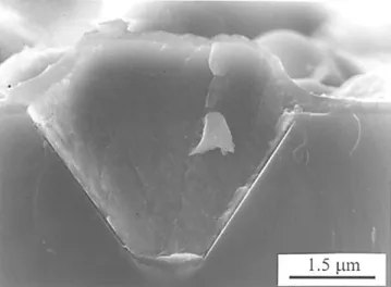
After annealing at 7008C, the surface layer of the Cu/TiB2/<Si> sample became completely discontinuous (Fig. 6c). Again, this struc-ture is very similar to the Cu/LPCVD TiB2/<Si> sample after failure of the TiB2barrier at 8008C.9After annealing at 8008C, surface mor-phology of the Cu/TiB2/<Si> sample was completely deteriorated (Fig. 6d). Irregular patches and rectangular crystallites had developed on the surface. The edges of rectangular crystallites are aligned along the <110> directions of the Si crystal (i.e., the natural cleavage lines). A SEM micrograph on the naturally fractured cross section of a 8008C-annealed sample shows a triangler-like crystallite with sharp edges penetrating into the Si substrate (Fig. 7). Similar features were frequently seen over the sample cross section. By using EDAX, we found that the triangular crystallite contained mostly Cu and a little Si. From the inclined angle of the edges, it is deduced that the crys-tallite is bounded by the Si{111} planes. Comparing the top-view and the cross-sectional micrographs (Fig. 6d and Fig. 7), we conclude that the rectangular crystallites in Fig. 6d take the form of inverted square pyramids. Therefore, their cross sections show a triangular structure, as seen in Fig. 7. These pyramids are analogous to the “pyramidal” spikes observed in the Al/<Si> system after annealing.20A similar pyramidal structure was also observed in the annealed Cu/Ta/<Si> system, and the pyramid was identified as Cu3Si.21In the present case, the pyramids should also be Cu3Si since EDAX reveals both Cu and Si within the pyramid and the major phase of the 8008C-annealed sample identified by XRD is Cu3Si (see below).
The chemical composition on the surface (10-30 Å deep) of the annealed Cu/TiB2/<Si> samples was further investigated by Auger electron spectrometry spot analysis. The samples were
sputter-cleaned by a 3 keV Ar ion beam for 5 min and then analyzed by AES, on the selected regions as marked by “A” to “G” in the SEM micro-graphs of Fig. 6. The results of the AES spot analysis, for elements of Cu, Si, and Ti (the boron signal was too weak to be detected) is listed in Table I. There is no Si signal detected on the surface of the sample after annealing at 6008C, even in the opening holes. The TiB2barrier consequently still preserved its integrity at 6008C. However, within the opening holes (region B), a Ti signal is detected. The Cu film left in the holes must be very thin such that Ti from the underneath barri-er laybarri-er was detected. Aftbarri-er annealing at 7008C, Cu, Ti, and Si all ap-peared on the island (region C) and open (region D) areas. After an-nealing at 8008C, the Cu signal was detected on the rectangular crys-tallites and the irregular patches (regions E and F), but not detected on the dark, open area (region G). Si signals were strong in all three re-gions. The reaction between Cu and Si substrate had clearly occurred when the samples were annealed at 700 and 8008C.
The glancing angle XRD spectra of the Cu/TiB2/<Si> samples before and after annealing at 600, 700, and 8008C are shown in Fig. 8. XRD reveals only diffraction peaks of Cu in the as-deposited Cu/TiB2/<Si> sample. Peaks for TiB2 is not observed since TiB2 layer is very thin and the grains are small. As seen in the figure, the spectrum of the 6008C annealed sample is similar to that of the as-deposited one, except for one extra peak at 2u < 538. This peak can-not be identified to any related Cu or Si compounds. For the 7008C spectrum, diffraction peaks of Cu3Si start to develop, but the Cu peaks are still significant. There is also an unidentified peak at 2u < 528 in this spectrum. The Cu3Si peaks become very distinct, and the Cu peaks seem to diminish for the sample after annealing at 8008C. This indicates that most of the Cu is transformed to Cu3Si at 8008C. There are also two small peaks of Cu2O phase observed in the 8008C spectrum. The X-ray diffraction result is in agreement with the AES spot analysis. Both results indicate that the reaction between Cu and Si had occurred when the sample annealed at 700 and 8008C. There-fore, the TiB2barrier had failed after annealing at 7008C for 30 min.
As a result, no evidence of reaction was observed in the sample after annealing at 6008C. The opening holes on the surface of the
Figure 7. A cross-sectional SEM of the Cu/TiB2/<Si> sample after
anneal-ing at 8008C in flowing 80%Ar 1 20% H2for 30 min.
Figure 8. XRD spectra of Cu/TiB2/<Si> samples before and after annealing
at 600-8008C for 30 min. (The peaks marked by * are those which cannot be identified as diffraction peaks of any related Cu or Si compounds.)
Table I. AES spot analysis on the surfaces of Cu/TiB2/<Si> samples after annealing at 600, 700, and 8008C for 30 min. Positions of the spots are marked in Fig. 6. (s, element detected; 3, element undetected.)
6008C 7008C 8008C
Element Point A Point B Point C Point D Point E Point F Point G
Cu s s s s s s 3
Si 3 3 s s s s s
6008C-annealed sample are attributed to the dewetting of Cu layer during heating because copper has a high surface energy. The sur-face energy of Cu at its melting point (10838C) is 1720 mJ/m2, while the surface energy of Al at its melting point (6608C) is only 1080 mJ/m2.22Consequently, thin Cu films will agglomerate easily at high temperatures. The dewetting of the Cu overlayer may be also related with the Cu-barrier interfacial energy, the surface energy of the barrier and the annealing atmosphere as well. The relationship between the dewetting of Cu layer and the subsequent failure of the barrier layer has yet to be elucidated.
In the literature, it had been reported that the Cu/LPCVD TiB2/<Si> system failed after annealing at 7758C for 30 min in vacu-um, according to the sheet resistance measurement.9In Ref. 9, the surface morphologies of the samples, before and after failure of the TiB2barrier, are very similar to the result in the present study. There was no AES or XRD analysis on the Cu/LPCVD TiB2/<Si> samples in that paper. However, from the surface morphology and the sheet re-sistance behavior, the stability of the metallization system in Ref. 9 seems to be 1008C higher than the current work. The TiB2films in Ref. 9 were deposited by LPCVD, with a stoichiometric composition and a fine grain size of 3 nm. The impurity content and the thickness of the TiB2barrier are not clearly specified. The variances in compo-sition, grain size, annealing ambient, and possibly the thickness of the TiB2barrier as well, will all contribute to the different performance in thermal stability of Cu/TiB2metallization system.
In the current work, we did not detect any apparent reaction be-tween Cu and TiB2, neither between Si and TiB2. The breakdown of the Cu/TiB2/<Si> system after heat-treatment shall mainly originate from the diffusion of Cu and/or Si via the grain boundaries of the TiB2barrier. The interdiffusion of Cu and Si induced by heat-treat-ment may start already after low-temperature annealing and result in consequent failure of devices. Therefore, the failure of real devices with TiB2barriers may occur long before the detection of change in sheet resistance or formation of Cu-Si compound. A more sensitive test, for example, the shallow junction diode leakage current test, should be performed to further evaluate the applicability of TiB2 bar-rier for Cu/<Si> system. Also, details in the failure mechanism re-mains to be investigated.
Conclusions
By co-sputtering from TiB2and boron targets and applying a neg-ative substrate bias of 200 V, we produced a nanocystalline TiB2film of 300 mV cm in resistivity. The TiB2film is slightly boron-rich and contains 5 atom % of oxygen. When a TiB2film of 60 nm in thick-ness is applied as a diffusion barrier between copper and the silicon substrate, no change in sheet resistance and no evidence of reaction are observed for the Cu/TiB2/<Si> samples annealed up to 6008C for 30 min. The appearance of opening holes on the surface of the 600 8C-annealed sample is attributed to the dewetting of copper films during heat-treatment. Sheet resistance of the Cu/TiB2/<Si> sample
increas-es by about five orders of magnitude after annealing at 700-8008C. The dramatic increase of the sheet resistance is associated with the deterioration of the surface and cross-sectional morphology, as well as the formation of Cu3Si compound. The 60 nm thick TiB2film thereby has failed as a diffusion barrier for Cu/<Si> metallization after heat-treatment at 7008C for 30 min. The failure mechanism may be associated with the diffusion of Cu and Si via the grain boundaries of the nanocrystalline TiB2barrier.
Acknowledgments
We thank Dr. S. J. Ding for the help in cross-sectional SEM work and R. C. Lee for technical assistance in AES analysis. Financial support for this work was provided by the National Science Council of Taiwan, R.O.C (contract no. NSC-88-2216-E-006-036) and by the Electronic Research and Service Organization at Industrial Technol-ogy Research Institute, Taiwan (contract no. 0387-B2036).
National Cheng Kung University assisted in meeting the publication costs of this article.
References 1. M.-A. Nicolet, Thin Solid Films, 52, 415 (1978).
2. D. Pramanik and V. Jain, Solid State Technol., 73 (Jan 1993).
3. S. Q. Wang, I. Raaijmakers, B. J. Burrow, S. Suthar, S. Redkar, and K. B. Kim, J. Appl. Phys., 68, 5176 (1990).
4. Ki-C. Park and K.-B. Kim, J. Electrochem. Soc., 142, 3109 (1995). 5. M. Mändl, H. Hoffmann, and P. Kücher, J. Appl. Phys., 62, 2127 (1990). 6. G. V. Samsonov and I. M. Vinitskii, Handbook of Refractory Compounds, p. 225,
IFI/Plenum, New York (1980).
7. CRC Handbook of Chemistry and Physics, 74th ed., D. R. Lide, Editor, p. 12-155, CRC Press, Boca Raton, FL (1993).
8. J. R. Shappirio, J. J. Finnegan, and R. A. Lux, J. Vac. Sci. Technol. B, 4, 1409 (1986).
9. C. S. Choi, G. A. Ruggles, A. S. Shah, G. C. Xing, C. M. Osburn, and J. D. Hunn, J. Electrochem. Soc., 138, 3062 (1991).
10. G. Sade and J. Pelleg, Appl. Surf. Sci., 91, 263 (1995).
11. S. N. Basu, K. M. Hubbard, J-P. Hirvonen, T. E. Mitchell, and M. Nastasi, Mater. Res. Soc. Symp. Proc., 187, 157 (1990).
12. J. R. Shappirio and J. J. Finnegan, Thin Solid Films, 107, 81 (1983).
13. C. S. Choi, G. C. Xing, G. A. Ruggles, and C. M. Osburn, J. Appl. Phys., 69, 7853 (1991).
14. L. M. Williams, Appl. Phys. Lett., 46, 43 (1985).
15. Handbook of X-Ray Photoelectron Spectroscopy, G. E. Muilenberg, Editor, Perkin-Elmer Corporation, Eden Prairie, MN (1979).
16. D. Briggs and M. P. Seah, Practical Surface Analysis, 2nd ed., pp. 599-606, John Wiley & Sons, Inc., New York (1983).
17. B. D. Cullity, Elements of X-Ray Diffraction, 2nd ed., p. 102, Addison-Wesley, Reading, MA (1978).
18. H.-O. Blom, T. Larsson, S. Berg, and M. Östling, J. Vac. Sci. Technol. A, 6, 1693 (1988).
19. E. Kolawa, P. J. Pokela, J. S. Reid, J. S. Chen, R. P. Ruiz, and M.-A. Nicolet, IEEE Electron Device Lett., 12, 321 (1991).
20. C. S. Pai, E. Cabreros, S. S. Lau, T. E. Seidel, and I. Suni, Appl. Phys. Lett., 47, 652 (1985).
21. J. Baumann, M. Stavrev, M. Rennau, T. Raschke, S. E. Schulz, C. Wenzel, C. Kauf-mann, and T. Gessner, Mater. Res. Soc. Proc. ULSI XIV, p. 321 (1999). 22. D. A. Porter and K. E. Easterling, Phase Transformation in Metals and Alloys,