The Influences of Moisture and Fluorine on the Characteristics
of Fluorinated Silicate Glass for Copper Metallization
Ching-Chun Chang,a Shiu-Ko JangJian,band J. S. Chena,
*
,z aDepartment of Materials Science and Engineering, National Cheng Kung University, Tainan, Taiwan b
Taiwan Semiconductor Manufacturing Company, Science-Based Industrial Park, Tainan, Taiwan
In this study, the impacts of moisture and unstable fluorine on the fundamental properties of fluorinated silicate glass共FSG兲 are discussed. Specific thermal treatment and water-soaking treatment are applied to the FSG dielectric layer. The influences of the moisture and fluorine outgassing from the FSG layers on the integrity of the Cu/TaNx⬃0.5/Ta/FSG/具Si典 multilayer structure are
investigated using transmission electron microscopy, Rutherford backscattering spectroscopy, and secondary ion mass spectros-copy. The results indicate that the formation of voids at the interface between the metallization layer and FSG film is correlated with the moisture and unstable fluorine in the FSG dielectric layer. Nevertheless, both of them can be eliminated by baking the FSG dielectrics prior to the subsequent metallization. Meanwhile, the dielectric constant and leakage current characteristics of the FSG film can be improved by driving out the moisture and unstable fluorine of the dielectric layer after baking in N2at ambient
conditions.
© 2006 The Electrochemical Society. 关DOI: 10.1149/1.2229278兴 All rights reserved.
Manuscript submitted March 10, 2006; revised manuscript received May 29, 2006. Available electronically July 28, 2006.
As the dimensions of the integrated circuits 共ICs兲 are scaled down continuously, the interconnect resistance–capacitance 共RC兲 time delay has become the dominant factor in determining the inter-connect performance. To reduce RC time delay, the traditional Al/SiO2structure is replaced by the Cu/low-k material below 90 nm
technology node. Several materials with low dielectric constants have been proposed in the literature, including poly-arylethers 共PAEs兲,1hydrogen silsesquioxane共HSQ兲,2fluorinated silicate glass
共FSG兲,3,4
organosilicate glass 共OSG兲,5and porous methylsilsesqui-oxane共MSQ兲.6To reduce the dielectric constant of SiO2-based
in-termetal dielectric共IMD兲, the introduction of carbon in the form of methyl 共CH3兲 groups and/or mesopores is effective to reduce the
dielectric constant from about 4 to a value less than 3. However, the mechanical strength can be significantly degraded, resulting in yield issues because of possible damage from subsequent chemical me-chanical polishing共CMP兲 processing steps.7Though the effective k value of FSG is slightly above 3, FSG has satisfactory mechanical strength such that it is still the most popular material with low di-electric constant used at the 90 nm technology node.
FSG possesses lower dielectric constant than SiO2 due to the
incorporation of fluorine into SiO2films.8The introduction of fluo-rine into SiO2leads to a less dense, more porous film by creating voids in the SiO2matrix. Meanwhile, the fluorine alters the
elec-tronic polarizability of the SiO2film.9The above two reasons con-tribute to a lower dielectric constant of the FSG dielectric layer. However, the drawbacks of doping fluorine into SiO2film, including
the increase of the number of interface traps and decrease of the adhesion strength of the metal/FSG interfaces, are the major con-cerns for using in the IC application.10,11According to our previous study, the FSG film is hydrophilic.12It indicates that moisture is absorbed by the FSG film as storing in the room ambient, and the absorbed moisture is released during thermal annealing. Moisture outgassing from the FSG layer is a serious issue, because it will degrade the integrity of IC circuits severely. Moisture in the FSG dielectric film also serves as the “water-related traps,” which result in the increase of the negative charges in the oxide layer.13 There-fore, in this study, to eliminate the deterioration caused by the fluo-rine and moisture, two kinds of thermal treatments are applied to the FSG films. The roles of fluorine and moisture in the FSG films and the influences of the thermal treatment on the dielectric layers are also discussed.
Experimental
The substrates used in the present study are p-type Si共100兲 wafers with resistivity of 8–12⍀ cm. The fluorinated silicate glass, 100 nm in thickness, was deposited onto silicon wafers in a single-wafer chemical vapor deposition 共CVD兲 chamber with SiH4
+ SiF4+ N2O. The dielectric constant of the FSG film measured
right after deposition is 3.7 by the mercury-probe method. After deposition, three types of FSG, denoted as FSGo, FSG*, and FSG”,
are prepared. FSGorepresents the FSG stored in the laboratory am-bient without any additional treatment before sputtering the metallic overlayers. FSG*denotes the FSG film with prebaking treatment at
400°C in N2ambient for 30 min before metallization. As for the FSG”, it indicates the FSG film prebaked in N2ambient at 400°C, soaked into deionized共DI兲 water for 30 min, and finally dried by N2. Sample nomenclature and pretreatment conditions of these
di-electrics are summarized in Table I. Ta, TaNx⬃0.5, and Cu layers were then deposited sequentially on the FSGoand FSG*dielectric layers by sputtering. Ta and TaNx⬃0.5layers were prepared by radio
frequency共13.56 MHz兲 sputtering, using a Ta metal target 共99.95% purity兲, and their thicknesses are 2 and 10 nm, respectively. The TaNx⬃0.5 film prepared with 1% of nitrogen flow ratio 关N2/共N2
+ Ar兲兴 has amorphous structure. More detailed information about the Ta–N films can be found in our previous work.14 Cu films 共180 nm兲 were then deposited on Ta–N films using dc sputtering with a Cu target共99.99% purity兲.
The Cu/TaNx⬃0.5/Ta/FSGo 共or FSG*兲/具Si典 共the symbol “具Si典”
represents the single-crystalline silicon substrate兲 samples were followed by postmetallization annealing 共PMA兲 in vacuum 共2.5 ⫻ 10−5Torr兲 at 400°C for 60 min to investigate the thermal
stabil-ity. High-resolution transmission electron microscopy 共HRTEM兲 was used to examine the reactions occurring at the Ta/FSG inter-faces. Compositional depth profile analysis was performed with Ru-therford backscattering spectrometry共RBS兲 and secondary ion mass spectroscopy 共SIMS兲. For RBS measurement, the4He+ ions were accelerated to 2 MeV and the backscattered ions were detected at a
*Electrochemical Society Active Member. z
E-mail: [email protected]
Table I. Sample nomenclature and summary of the pretreatment applied on the FSG films. “䊊” indicates that the specific treat-ment was performed on the dielectric film, while “Ô indicates that the dielectric film did not receive the treatment.
Sample FSGo FSG* FSG”
Pretreatment
Baked at 400°C in N2ambient for 30 min ⫻ 䊊 䊊
scattering angle of 160°. SIMS analysis was performed using Cs+
primary ion beam. To avoid knock-on effect, the Cu layer was stripped by acid solution before SIMS analysis. The acid solution is composed of phosphorous, nitric acid, and acetic acid mixed in a proportion of 1:1:1. Water desorption from the dielectrics was ana-lyzed by thermal desorption spectroscopy共TDS兲.
To obtain the electrical characteristics of the dielectric films, Cu/FSG/具Si典 metal-oxide-semiconductor 共MOS兲 capacitors were fabricated. Copper of 200 nm in thickness was sputtered through a shadow mask to obtain circular dots of 0.4 mm diam. To calculate the dielectric constant 共k兲 of the dielectric, capacitance–voltage 共C–V兲 measurement was performed using an HP 4284 LCR meter at a frequency of 100 kHz with an ac small signal of 25 mV. The leakage current densities of the dielectric films prepared by various conditions were also characterized using a computer-controlled HP 4140B pA meter/dc voltage source with a staircase-ramped voltage stress for current–voltage 共I–V兲 curves. The refractive indices of FSG films were determined using an ellipsometer共Woollam M-44兲. A broad band共450–700 nm兲 of light from a Xe arc lamp was lin-early polarized and directed onto the film surface at an angle of 75° to the surface normal. The change in polarization and reflectance of the reflected beam was measured through a rotating analyzer and then detected. To clarify the effects of the thermal treatment on the Si-bonding characters of the dielectrics, infrared 共IR兲 absorption spectra of the FSGo, FSG*, and FSG” films, as-prepared and after annealing at 400°C in vacuum for 60 min, were measured by a transmission Fourier transform infrared spectrometer共FTIR兲 rang-ing from 400 to 4000 cm−1operated in the absorbance mode with a
Jasco 460 FTIR spectrometer. The acquisition number of each FTIR spectrum was 128 with resolution of 4 cm−1, where the spectrum
were taken with the background subtracted by a standard bare sili-con wafer.
Results and Discussion
Figure 1 depicts cross-sectional TEM bright-field micrographs of the Cu/TaNx⬃0.5/Ta/FSGo/具Si典 and Cu/TaNx⬃0.5/Ta/FSG*/具Si典
multilayer structures, which are as-deposited and after PMA at 400°C in vacuum for 60 min. The FSG without prebaking process is denoted as FSGoand denoted as FSG*with prebaking treatment
共400°C/30 min, in N2兲 in this study. Figure 1a and b indicate that
the interfaces between the TaNx⬃0.5/Ta bilayers and the dielectric films of the as-deposited samples are smooth, and the barrier layers adhere well to the dielectric films for both FSGo and FSG*. How-ever, after PMA, voids can be observed at the interface between TaNx⬃0.5/Ta bilayer and FSGo film共Fig. 1c兲 but cannot be found
between TaNx⬃0.5/Ta and FSG*layer共Fig. 1d兲. The average size of
voids is about 20 nm. The origin of these voids is further explored and discussed as follows.
The compositional depth profiles of the Cu/TaNx⬃0.5/Ta/FSGo
共or FSG*兲/具Si典 specimens, as-deposited and after PMA, were
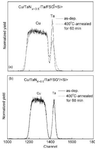
inves-tigated by RBS and the spectra are shown in Fig. 2. Figure 2a gives the comparison of RBS spectra for the Cu/TaNx⬃0.5/Ta/FSGo/具Si典
specimens, deposited and after PMA. Compared to the as-deposited spectrum, the Cu profile in the 400°C/60 min annealed spectrum become more slanted, and so does the Ta profile. This implies that interdiffusion had occurred at both the Cu/TaNx⬃0.5and Ta/FSGo interfaces after PMA. Nevertheless, for the FSG* speci-mens, the profile of the as-deposited sample overlaps nicely with that of the annealed sample共Fig. 2b兲. The RBS result proves that prebaking on the FSG dielectric layer improves the thermal stability of the multilayer structure significantly and helps to prevent Cu and Ta from interdiffusing.
It had been reported that Cu diffuses rapidly into dielectrics pri-marily due to oxidation of copper caused by the moisture absorbed in the dielectric film.15,16Additionally, the cross-sectional TEM im-age共Fig. 1c兲 reveals the formation of voids at the interface between TaNx⬃0.5/Ta bilayer and the FSGofilm after PMA. To clarify if the
TEM and RBS results correlate with the moisture contained in the dielectrics, FSG single layer 共FSGo and FSG*兲 were analyzed by thermal desorption spectroscopy共TDS兲. A constant heating rate of 20°C per minute was used during the measurement. The mass-to-charge ratio共m/e兲 = 18, corresponding to water 共H2O兲 molecules, was recorded. The TDS result of water desorption from the FSGo and FSG* films is shown in Fig. 3. A blank Si wafer was also
Figure 1. Cross-sectional TEM micrographs of 共a兲 as-deposited Cu/TaNx⬃0.5/Ta/FSGo/具Si典, 共b兲 as-deposited Cu/TaNx⬃0.5/Ta/FSG*/具Si典, 共c兲
400°C/60 min annealed Cu/TaNx⬃0.5/Ta/FSGo/具Si典, and 共d兲 400°C/60 min
annealed Cu/TaNx⬃0.5/Ta/FSG*/具Si典.
Figure 2. RBS spectra of the 共a兲 Cu/TaNx⬃0.5/Ta/FSGo/具Si典 and 共b兲
Cu/TaNx⬃0.5/Ta/FSG*/具Si典 specimens, as-deposited and after annealing at
investigated as a reference. Figure 3 demonstrates that the FSGofilm
contains a significant amount of water, whereas the FSG*dielectric
layer does not. Degradation of the multilayer, as shown by TEM and RBS analysis, is thus connected with moisture absorbed in the FSG layer.
To understand the impacts of moisture on the chemical compo-sition of FSG, the FTIR absorption spectra of the FSGo films,
as-prepared and after annealing at 400°C in vacuum and in N2ambient,
is shown in Fig. 4. It has been reported that absorbed H2O in
dielec-tric film shows a broadband at 3400–3200 cm−1.17Therefore, the
appearance of a wide peak centered around 3350 cm−1is associated with the vibration of Si–OH bonds in the as-prepared FSGofilm. A
minor peak located around 3650 cm−1is also observed and it should
be attributed to the OH stretching vibration in Si–OH bonds.18 How-ever, it can be found that the Si–OH bonds disappear after annealing of FSGoin vacuum and in N
2ambient. This indicates that the
ab-sorbed water in the FSGofilms are driven out after thermal
treat-ment.
Because the role of moisture in degradation of the multilayer structure has been confirmed, the degradation caused by the “un-stable fluorine” is discussed in the next section. In this study, the unstable fluorine indicates the weakly bonded or unbonded fluorine in the FSG film which is released from the dielectric layer after
thermal annealing.19Therefore, we would like to discuss the influ-ences of prebaking treatment on the stability of fluorine content in the Cu/TaNx⬃0.5/Ta/FSGo共or FSG*兲/具Si典 structure.
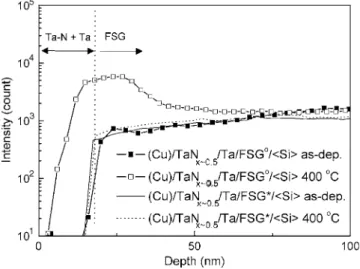
Figure 5 shows the SIMS depth profiles of F signals of various 共Cu兲/TaNx⬃0.5/Ta/FSGo共or FSG*兲/具Si典 specimens. The “共Cu兲”
symbol denotes that Cu films on the multilayer specimens had been removed by acid solution before performing SIMS analysis. In Fig. 5, we can find an accumulation of F at the Ta/FSGointerface of the
共Cu兲/TaNx⬃0.5/Ta/FSGo/具Si典 specimen due to the high reactivity of
Ta with F. We have demonstrated that tantalum fluoride forms at the Ta/FSGointerface after annealing at 400°C, observed by X-ray
pho-toelectron spectroscopy共XPS兲.12It had been reported that the inter-action between the Ta layer and unstable fluorine released from the dielectric layer affects the adhesion by occupying the dangling bonds at the interface.20Nevertheless, the profile of F signals in the FSG*film remains similar even after annealing at 400°C for 60 min.
SIMS analysis suggests that prebaking treatment “stabilizes” the FSG film. The desorption of fluorine from FSG films has also been measured by TDS analysis 共not shown兲 at temperatures ranging from room temperature to 800°C. It is found that the amount of fluorine driven out from the FSG films decreases drastically after prebaking treatment in N2 and reduces further after annealing in
vacuum. Though the exact amount of fluorine driven out cannot be quantified, the result indicates that, besides residual moisture, un-stable fluorine in the FSG film is also driven out by prebaking at 400°C in N2ambient for 30 min prior to the subsequent
metalliza-tion. Accordingly, the interaction between the metallization layer and unstable fluorine can be prevented effectively. Meanwhile, the degradation of the specimens via outgassing are reduced signifi-cantly.
To further understand the characteristics of Si–O and Si–F bonds in the FSG dielectric layers, Fig. 6 shows the FTIR absorption spec-tra of the FSGo, FSG*, and FSG” films as-prepared and after
anneal-ing at 400°C in vacuum. In Fig. 6, the spectra exhibit the absorption peaks around 810, 935, and 1085 cm−1, which are corresponding to
the Si–O bending vibrational mode关denoted by Si–O共b兲兴, the Si–F stretching vibrational mode 关denoted by Si–F共s兲兴, and the Si–O stretching vibrational mode关denoted by Si–O共s兲兴, respectively.21It could be found that the peak position of Si–O共s兲 mode shifted slightly to the higher frequency side共blueshift兲 after thermal treat-ment, which suggests a reduction of film density共discussed later兲.
The relative content of Si–F bonds in the FSG films is calculated by the ratio of peak height of the Si–F stretching mode to the Si–O Figure 3. TDS spectra of FSGo and FSG* films showing the H
2O+
共m/e = 18兲 ion yield vs temperature. The TDS spectrum of a blank Si wafer is also shown as a reference.
Figure 4. FTIR spectra of the FSGo films before and after annealing at
400°C in vacuum and in N2ambient. The region of wave numbers
corre-sponding to the vibrational frequencies of Si–OH and H2O is indicated.
Figure 5. SIMS profiles of the F signals in the共Cu兲/TaNx⬃0.5/Ta/FSGo共or
FSG*兲/具Si典 specimens, as-deposited and after annealing in vacuum at 400°C
for 60 min.关Note: 共Cu兲 indicates that the Cu layer had been removed before performing the SIMS analysis.兴
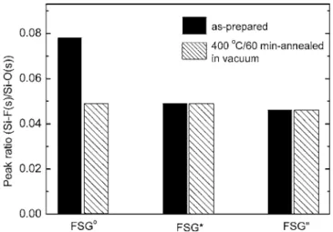
stretching mode and illustrated in Fig. 7. It shows that significant reduction in the relative content of the Si–F bonds can be found after thermal treatment. In Fig. 7, the relative 关Si–F共s兲/Si–O共s兲兴 peak ratios of the FSG films with thermal treatment共prebaking or 400°C/60 min annealing兲 are about half of the magnitude as com-pared with the FSGofilm. The result indicates that unstable fluorine
is driven out after thermal treatment, which is consistent with the TDS analysis. Consequently, there is no fluorine piling up at the Ta/FSG interfaces of the prebaked FSG films共FSG*兲, as shown in
Fig. 5.
As we know, the motive of introducing low-k material into IC interconnection is to reduce RC time delay. The RC delay means the signal-propagating time delay which is approximately 0.89RC, where R is the line resistance and C is the total capacitance associ-ated with the line.22Therefore, the variation in the dielectric con-stants of the dielectrics caused by thermal treatment should be an important concern. In this study, the dielectric constants共k兲 of the FSG films, with thermal treatment or not, are calculated from the capacitance of Cu/FSGo共or FSG*兲/具Si典 MOS structure at the
accu-mulation mode. Furthermore, to clarify the effects of water
absorp-tion on the electrical properties of FSG, the FSG” film共prebaked at 400°C in N2ambient for 30 min followed by soaking in DI water for 30 min兲 were also prepared and investigated. Whereas the un-stable fluorine has been driven out from the FSG films by prebaking treatment, the effects caused by the trapped H2O molecules on the
electrical properties of the FSG films can be confirmed by compar-ing the results of FSG*with those of FSG”.
Table II summarizes the dielectric constants of the FSGo, FSG*,
and FSG”, before and after annealing at 400°C in vacuum for 60 min. Meanwhile, the standard deviation numbers for the dielec-tric constant values are also included. According to Table II, we can find the dielectric constant of the FSGofilm, which is stored in the
laboratory ambient and without any thermal treatment, is 4.6. This value is much higher than the dielectric constant of the FSG mea-sured right after deposition共⬃3.7兲 and is even higher than that of thermal oxide 共⬃4.0兲. Nevertheless, the k value of the 400°C/60 min annealed FSGowould be reduced drastically to 3.6.
This indicates that the dielectric constant of FSG increases easily as it is stored in the room ambient, but, after annealing at 400°C for 60 min, the dielectric constant of FSGo is lowered. Table II also indicates that the k value of the as-prepared FSG* 共3.8兲 is much
closer to the value of the as-deposited FSG共3.7兲. However, the k value of FSG*could be reduced even as low as 3.2 after annealing in vacuum for 60 min, which is smaller than the k value of as-deposited FSG. Because the unstable fluorine has been driven out of FSG*after baking, the further reduction in the k value of the FSG*
layer implies that the dielectric constant is not determined by the unstable fluorine in the film but by some other factors which are discussed later. It includes the content of the moisture in the dielec-tric film and/or the film density of the dielecdielec-tric layer. This obser-vation is similar to the conclusion reported by Fujii et al.19
To enhance the amount of H2O molecules in FSG film and pro-hibit the influence caused by fluorine, the FSG film with prebaking treatment is followed by immersing it into DI water for 30 min and denoted as FSG”. The dielectric constant of as-prepared FSG”, listed in Table II, is 4.2 and reduces to 3.5 after annealing at 400°C for 60 min. Both FSG*and FSG” are prebaked, and the only diversity is
the water content in the films. By comparing the k value of the as-prepared FSG” film with that of the as-prepared FSG*, the
in-crease of the dielectric constant of the FSG” film can be attributed certainly to the moisture absorption. Because the dielectric constant of water is large共⬃80 at room temperature兲, the presence of H2O molecules in the dielectric layer would increase the k value obvi-ously. Moreover, H2O molecules reacting with the unstable Si–F
bonds create Si–OH and hydrofluoric共HF兲 bonds and change the ionic polarization of the FSG film, leading to the increase of the dielectric constant.23
By comparing the k values of as-prepared FSGo 共4.6兲, FSG*
共3.8兲, and FSG” 共4.2兲, it is clear that the main factor altering the k values of FSG is the moisture content. Prebaking 共400°C in N2 ambient for 30 min兲 treatment is effective in driving the moisture out of the dielectrics and the water-soaking process brings the mois-ture back. Nevertheless, the 400°C/60 min annealing further re-duces the k values to be even lower than that of as-deposited FSG 共⬃3.7兲. By using an ellipsometer, we have realized that the refrac-tive index of the as-prepared FSGois 1.464 and it becomes 1.447 after annealing at 400°C for 60 min. In principle, refractive indices Figure 6. FTIR spectra of FSGo, FSG*, and FSG” films as-prepared and
after annealing at 400°C in vacuum for 60 min. The Si–O stretching, Si–O bending, and Si–F stretching vibrational modes are labeled as Si–O共s兲, Si–O共b兲, and Si–F共s兲, respectively.
Figure 7. Variation of共Si–F共s兲/Si–O共s兲兲 FTIR peak ratios of the FSGo,
FSG*, and FSG” films, as-prepared and after annealing at 400°C in vacuum
for 60 min.
Table II. k values and standard deviation (SD) of various FSG films as-prepared and after annealing at 400°C in vacuum for 60 min.
FSGo FSG* FSG”
k SD k SD k SD
As prepared 4.6 0.1 3.8 0.1 4.2 0.1
of the materials with similar composition are proportional to the density. It indicates that the film density of the FSG films decreases after annealing. Reduction of film density can also be deduced from an examination of FTIR spectra共Fig. 6兲, which shows the blueshift of the Si–O共s兲 vibrational mode after thermal treatment. Lucovsky et al. had reported that the blueshift of the Si–O stretching mode was caused by the decrease in the film density.24Accordingly, both FTIR and elliposometry analyses suggest that the density of the FSG films decreases after annealing, which consequently leads to the reduction in the dielectric constant of the 400°C/60 min annealed FSG films. The decrease of film density may be due to the loss of fluorine and/or the instability of the FSG structure.25
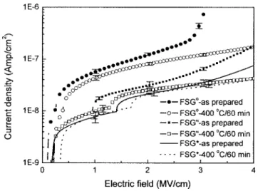
Figure 8 shows the leakage current density vs electric field共J–E兲 curves of the Cu/FSG/具Si典 MOS capacitors. Ten samples at least were used for the evaluation of leakage current density in each case and the standard deviation error was indicated in Fig. 8 in the elec-tric fields of 1, 2, and 3 MV/cm. According to the magnitude of the leakage current density, these J–E curves can be divided into two groups. The first group includes the FSGosamples only; the second
group includes FSG*and FSG” samples. The results indicate that
the leakage current densities of the FSGofilms are higher by 1 order
of magnitude than those of the prebaked 共400°C/30 min, in N2兲
FSG*and FSG” films. It had been reported that weak Si–F bonds
共the origin of the unstable fluorine兲 in the FSG film become trapping centers of charges and result in the increase of the leakage current of the MOS capacitors.10,26In addition, the Si–OH bonds in the FSG film also increase the leakage current. In this study, it is shown that the unstable fluorine can be reduced共i.e., eliminating the weak Si–F bonds兲 after annealing in N2ambient and in vacuum. However, it is
noticed that the N2ambient-annealed FSG films共FSG*and FSG”兲
possess lower leakage current densities as compared to the vacuum-annealed FSG samples共FSGo兲 共shown in Fig. 8兲. The principal
re-sidual gas in a vacuum共2.5 ⫻ 10−5Torr兲 is just H2O vapor; thus,
annealing of FSG in vacuum共2.5 ⫻ 10−5Torr兲 is the same as
an-nealing of FSG in low-pressure H2O vapor. The superiority of pre-baking of FSG in nitrogen to annealing of FSG in vacuum 共2.5 ⫻ 10−5Torr兲 is due to the possibility that there is less moisture in
the prebaking ambient. By comparing the J–E curve of as-prepared FSG*with that of as-prepared FSG” shown in Fig. 8, it can be found
that the leakage current density of FSG*film is slightly smaller than
that of the FSG” sample. The only difference between FSG*and FSG” is the water content in the dielectric films, and it also indicates
that moisture is the main factor in determining the leakage current. The leakage current density of the FSG film increases as water mol-ecules are absorbed in the FSG dielectric layer.
Conclusion
This study investigates the influences of moisture and unstable fluorine on the properties of the FSG dielectric layer and the integ-rity of the Cu/TaNx⬃0.5/Ta/FSG/具Si典 multilayer structure. The re-sults indicate that the moisture absorbed in the FSG film increases the dielectric constant drastically. Furthermore, leakage current den-sity of the FSG dielectric layer is affected by the moisture content in the dielectric layer. In this study, both prebaking in N2ambient and annealing in vacuum can reduce the leakage current densities of the FSG films. However, the effect of prebaking treatment in N2 ambi-ent is superior to that of annealing the FSG film in vacuum. This should be attributed to the less moisture as baking in N2 ambient
than annealing in vacuum共2.5 ⫻ 10−5Torr兲. This study shows that
the outgassing process might deteriorate the performance of the IC devices. Therefore, baking the FSG dielectric adequately prior to the subsequent metallization is essential.
Acknowledgments
The authors gratefully acknowledge the financial support from the National Science Council of Taiwan共grant no. NSC-94-2216-E-006-033兲. They also are greatly indebted to the Nuclear Science Technology Development Center at National Tsing Hua University, Taiwan for RBS facilities.
National Cheng Kung University assisted in meeting the publication costs of this article.
References
1. R. N. Vrtis, K. A. Heap, W. F. Burgoyne, and L. M. Robeson, Mater. Res. Soc. Symp. Proc., 443, 171共1997兲.
2. T. E. F. M. Standaert, P. J. Matsuo, S. D. Allen, and G. S. Oehrlein, J. Vac. Sci. Technol. A, 17, 741共1999兲.
3. S. W. Lim, Y. Shimogaki, Y. Nakano, and K. Tada, Appl. Phys. Lett., 68, 832 共1996兲.
4. S. M. Han and E. Aydil, J. Vac. Sci. Technol. A, 15, 2893共1997兲. 5. M. J. Loboda, Microelectron. Eng., 50, 15共2000兲.
6. A. T. Kohl, R. Mimna, R. Shick, L. Rhodes, Z. L. Wang, and P. A. Kohl, Electro-chem. Solid-State Lett., 2, 77共1999兲.
7. T. C. Chang, P. T. Liu, T. M. Tsai, F. S. Yeh, T. Y. Tseng, M. S. Tsai, B. C. Chen, Y. L. Yang, and S. M. Sze, Jpn. J. Appl. Phys., Part 1, 40, 3143共2001兲. 8. M. J. Shapiro, S. V. Nguyen, T. Matsuda, and D. Dobuzinsky, Thin Solid Films,
270, 503共1995兲.
9. S. M. Han and E. S. Aydil, J. Appl. Phys., 83, 2172共1998兲.
10. L. Tsetseris, X. J. Zhou, D. M. Fleetwood, R. D. Schrimpf, and S. T. Pantelides, Appl. Phys. Lett., 85, 4950共2004兲.
11. G. R. Yang, Y. P. Zhao, B. Wang, E. Barnat, J. McDonald, and T. M. Lu, Appl. Phys. Lett., 72, 1846共1998兲.
12. C. C. Chang, S. K. JangJian, and J. S. Chen, J. Electrochem. Soc., 152, G517 共2005兲.
13. E. H. Nicollian and J. R. Brews, MOS Physics and Technology, John Wiley & Sons, New Jersey共2003兲.
14. C. C. Chang, J. S. Jeng, and J. S. Chen, Thin Solid Films, 413, 46共2002兲. 15. P. T. Liu, T. C. Chang, Y. L. Yang, Y. F. Cheng, and S. M. Sze, IEEE Trans.
Electron Devices, 47, 1733共2000兲.
16. O. R. Rodriguez, W. Cho, R. Saxena, J. L. Plawsky, and W. N. Gill, J. Appl. Phys., 98, 024108共2005兲.
17. W. A. Pliskin, J. Vac. Sci. Technol., 14, 1064共1977兲.
18. S. Kondo, K. Tomoi, and C. Pak, Bull. Chem. Soc. Jpn., 52, 2046共1979兲. 19. T. Fujii, K. Asai, M. Sawada, K. Sakurai, K. Kobayashi, and M. Yoneda, J.
Elec-trochem. Soc., 152, G152共2005兲.
20. Y. S. Kim and Y. Shimogaki, J. Vac. Sci. Technol. A, 19, 2642共2001兲. 21. S. H. Lee and J. W. Park, J. Appl. Phys., 80, 5260共1996兲.
22. J. D. Plummer, M. D. Deal, and P. B. Griffin, Silicon VLSI Technology, p. 682, Prentice Hall, New Jersey共2000兲.
23. M. Yoshimaru, S. Koizumi, and K. Shimokawa, J. Vac. Sci. Technol. A, 15, 2915 共1997兲.
24. G. Lucovsky, M. J. Manitini, J. K. Srivastava, and E. A. Irene, J. Vac. Sci. Technol. B, 5, 530共1987兲.
25. G. Ceriola, F. Iacona, F. L. Via, V. Raineri, E. Bontempi, and L. E. Depero, J. Electrochem. Soc., 148, F221共2001兲.
26. W. J. Chang, M. P. Houng, and Y. H. Wang, Jpn. J. Appl. Phys., Part 1, 40, 1300 共2001兲.
Figure 8. J–E curves of Cu/FSGo/具Si典, Cu/FSG*/具Si典, and Cu/FSG”/具Si典
MOS capacitors, for the dielectrics as-prepared and after annealing in vacuum at 400°C for 60 min. The standard deviation error bars are also indicated on each curve at the electric fields of 1, 2, and 3 MV/cm.