Resistive Switching Behaviour of Diode-like gadolinium oxide
Resistive Random Access Memory
C.H Wu1*, Y.D Ho1, and C.L Huang1
1
Department of Electrical Engineering, National Cheng Kung University, 1 University Road, Tainan 70101, Taiwan
*Corresponding author: Email [email protected]
Abstract Summary: The diode-like Al/Gd2O3/Si/Al resistive random access memory
(RRAM) shows a forming-free and bipolar resistive switching behaviour after N2-H2
annealing. In addition, our sample has the largest and more stable resistive switching window at 800oC.
Introduction: Recently, RRAM based on transition metal oxides (TMOs) was considered as the next generation non-volatile memory devices for their fast switching speed, low-power operation and high density integration. However, TMOs required forming process to obtain the stable RS which need large bias voltage resulting in unpredictable resistance states [1]. Therefore, we need to replace the TMOs which can perform without forming. Gd2O3 has been found that it has sufficient defects itself so that it can perform better RS
without forming [2] and also regarded as n-type material [3]. Moreover, Gd2O3 has high
dielectric constant, larger band gap and thermal stability on silicon. In the general RRAM structure, it is often to use crossbar array structure for high-density storage. However, this cross array design results in crosstalk phenomenon. That is, the sneak current will pass through the adjacent cells which have no rectifying performance leading to misreading problem [4]. In this work, using p-Si to reduce the leakage current and combine with nearly n-type Gd2O3 thin film was regarded as one p-n diode that had rectifying behaviour. We
want to find the better procedure conditions to obtain the better RS properties in diode-like RRAM.
Experiment: The Gd2O3 thin film was deposited on p-Si by sputtering with 6 sccm Argon
at substrate temperature 400oC using Gd2O3 target. After annealing with 600-800oC, the Al
top electrode of 1000μm in diameter was deposited by e-beam evaporator to measure the electrical properties of Gd2O3 thin film. The RRAM structure is shown in Fig. 1. The crystal
structure was examined by XRD and the XPS was employed to analysis the chemical bonding state of Gd2O3 thin film. The electrical properties are measured by Agilent E5270B
Parameter Analyzer.
Results and discussions: It is found that the secondary phase doesn’t exist in Gd2O3 film
by the XRD (not shown here). Fig. 2 shows the typical I-V characteristics of Al/Gd2O3/Si/Al
structure after annealing at 600-800oC. At 800oC, bipolar RS behaviour appears because there is more oxygen vacancy generating in the Gd2O3 film with increasing annealed
temperature at N2-H2 atmosphere. In bipolar RS, oxygen vacancies are driven by the
electric field and considered as the conductive filaments [5]. Hence, the resistance value changes from high resistance state (HRS) to low resistance state (LRS) under the forward bias, vice versa. In our work, the devices keep in HRS under reverse bias due to the rectification on n-Gd2O3/p-Si suppressed the current flows. The RS window and operated
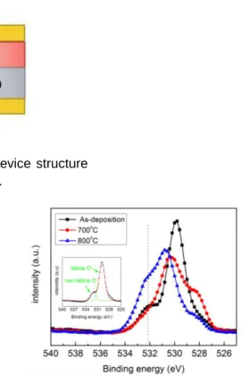
voltage can be improved through post-metallization annealing 300oC (as shown in the inset of Fig. 2). In order to confirm the RS mechanism is by oxygen vacancy, XPS analysis was performed to examine the existence of non-lattice and lattice oxygen ions. In the inset of Fig. 3, the O 1s signal of as-deposited Gd2O3 film comprises two peaks, the lattice
oxygen ions at about 530 eV and non-lattice oxygen ion at about 532 eV [1, 2]. It is found that the intensity of non-lattice oxygen ion had no change at 700oC but increased at 800oC in Fig. 3. Hence, it can suppose that there is no obvious variation in the amount of oxygen vacancies under the 800oC. Besides, the binging energy would increase due to oxygen
vacancies increasing under 800oC N2-H2 annealing. As a result, it is reasonable that the
RS behaviour is much better than 600oC and 700oC.
Conclusion: We found the better procedure for Al/Gd2O3/Si/Al RRAM device. It has the
better RS property at annealing 800oC with N2-H2 atmosphere due to more oxygen
vacancy. The bipolar behaviour can be attributed to the oxygen vacancy in the Gd2O3 film
as the annealing temperature increases. The rectified current ratio of LRS is about three orders of magnitude. This is the potential of diode-like RRAM not only on suppressing crosstalk but having better RS property.
Acknowledgements
This work has been supported by the Australian Research Council. This work was financially supported by the National Science Council of Taiwan under grant NSC 100-2221-E-006-124-MY3. The experimental work was performed at Center for Micro/Nano Science and Technology, National Cheng Kung University and VLSI Thin Film Lab.
References
[1] T.M. Pan and C.H. Lu, “Forming-free resistive switching behavior in Nd2O3, Dy2O3, and Er2O3 films
fabricated in full room temperature,” Appl. Phys. Lett., vol. 99, pp. 113509-1–3, September 2011. [2] T.M. Pan and C.H. Lu, “Switching behavior in rare-earth films fabricated in full room temperature,” IEEE
transactions on electron devices, vol. 59, pp. 956–961, April 2012.
[3] J.C. Wang, Y.R. Ye, J.S. Syu, P.R. Wu, C.I Wu, P.S. Wang, and J.H. Chang, “Low-power and high-reliability gadolinium oxide resistive switching memory with remote ammonia plasma treatment”, Japanese Journal of Applied Physics, vol. 52, pp. 04CD07-1–4, March 2013
[4] M.Y. Song, Y. Seo, Y.S. Kim, H.D. Kim, H.M. An, B.H. Park, Y.M. Sung, and T.G. Kim, “Realization of One-Diode–Type Resistive-Switching Memory with Cr–SrTiO3 Film,” Applied Physics Express, vol. 5, pp. 091202-1–3, August 2012.
[5] K.L. Lin, T.H. Hou, J. Shieh, J.H. Lin, C.T. Chou and Y.J. Lee, “Electrode dependence of filament formation in HfO2 resistive-switching memory,” J. Appl. Phys., vol. 109, pp. 084104-1–7, April 2011.
Fig. 1. The schematic device structure of Al/Gd2O3/Si/Al RRAM.
Fig. 2. Typical I-V characteristics of Al/Gd2O3/Si/Al structure at 600
o
C-800oC. The inset shows I-V characteristics of Al/Gd2O3/Si/Al structure at 800
o
C before and after post-metalization annealing.
Fig. 3. XPS of O 1s for the Gd2O3 film with
as-deposited and annealed 700-800oC. The inset shows XPS spectra of O 1s with non-lattice and lattice binding energy.