Electroless Deposition of Cu Thin Films with CuCl
2-HNO
3Based Chemistry
II. Kinetics and Microstructure
Wei-Tsu Tseng,*, a, zChia-Hsien Lo, and Shih-Chin Lee
Department of Materials Science and Engineering, National Cheng-Kung University, Tainan 701, Taiwan
This paper describes the kinetics involved in the acid-based electroless Cu deposition system employing CuCl2-HNO3chemistry in a HF-NH4F buffer solution. The rate equation is set up as a function of concentrations of active chemical components involved, and rate orders are determined to evaluate the contribution from each component. The deposition rate of Cu is found most sensitive to variation in关Cl⫺兴 concentrations, followed by that of 关Cu2⫹兴 and 关F⫺兴. The activation energy derived from deposition at different temperatures is 0.445 eV. Grain size of deposited Cu films is influenced strongly by deposition rate. Electrical resistivity of Cu films is dominated by the amount of point defects and microvoids present right after deposition, and by grain size after a 300°C anneal.
© 2001 The Electrochemical Society. 关DOI: 10.1149/1.1359201兴 All rights reserved.
Manuscript submitted October 11, 2000; revised manuscript received January 8, 2001.
Electroless plating provides a viable alternative to electroplating for Cu thin-film deposition in the era of Cu-based multilevel inter- connect for microelectronic devices.1Besides its capability of filling high-aspect-ratio pattern structure, electroless plating offers addi- tional advantages such as low cost and simpler chemistry.
Most existing electroless Cu plating processes adopt base solu- tions with copper sulfate as the Cu ion source, ethylenedinitroloac- etate
共EDTA兲 as the complexing agent, formaldehyde as reducing
agents, tetramethylammonium hydroxide共TMAH兲 or alkali solution
as pH buffer, and some surfactant and stabilizer added to improve step coverage and bath stability, respectively. This chemical formu- lation has been studied extensively over the past twenty years and has been applied to the manufacture of circuit boards.In the first part of this study,2 we proposed an acid-based CuCl2-HNO3electroless Cu plating solution with HF-NH4F as pH buffer. An optimum deposition rate of
⬃2700 Å/min directly on
TaN substrate and a resistivity of 2.35⍀ cm can be achieved at pH
4.70. CuCl2, when dissolved in the solution, provides the关Cu
2⫹兴
ions, which are catalyzed by HNO3on TaN surface and reduced by Si to form Cu deposits.关Cl
⫺兴 and 关F
⫺兴 ions act as complexing
agents and transmit the electrons from Si to关Cu
2⫹兴. Cu deposition
rate exhibits a decreasing trend with increasing关HNO
3兴 concentra-
tion in the bath. Adding关HF兴 or 关NH
4F兴 into the bath, on the other
hand, enhances the deposition rate to a peak level, after which it saturates and declines.As an extension of our previous study, we explore the kinetics and material issues of the system in this contribution. Concentration of the active components and temperature used in the system are varied in order to deduce the reaction rate orders and activation energy. Evolution of grain size and resistivity with
关Cu
2⫹兴 concen-
tration in the chemical bath are analyzed. The effects of postdepo- sition anneal on resistivity, microstructure, and preferred crystal ori- entation of Cu thin films are also investigated.Experimental
Determination of reaction rates.—Chemical components and substrate materials used for the Cu deposition experiment basically follow those from our previous study.2A brief description is pre- sented here. 100 mm p-type
共1.7-2.5 ⍀ cm resistivity兲 具100典 Si
wafers are thermally oxidized in dry atmosphere to produce an oxide thickness of 100 nm. 50 nm Ta and 50 nm TaN are then depositedonto the oxide surface consecutively by dc magnetron sputtering in Ar and N2ambient. The thickness of the Ta/TaN films is measured by four-point probe resistance measurement and calibrated with cross-sectional scanning electron microscopy
共SEM兲. The resistivity
of Ta and TaN films is 175 and 242⍀ cm, respectively. To deter-
mine the reaction rates, these Ta/TaN/Si wafers are cut into 1⫻ 1 cm pieces as substrate. The weight difference before and after
5 min immersion of the substrates into the bath was recorded. In this case the deposition rate was expressed in units of mg/min cm2. Bath temperature and concentration of the active chemical components in the bath were varied in order to deduce the reaction kinetics. Split conditions used for this set of experiments are summarized in Table I.Effects of dilution on Cu deposition rate.—Too fast a deposition rate often leads to microvoid formation within the Cu microstruc- ture. To compensate for this drawback, deionized
共DI兲 water was
added to dilute the bath and its effects on deposition rate and mi- crostructure were monitored. For this set of experiments the bath originally consisted of 20 g NH4F, 30 mL HF, 20 mL HNO3, 1.62 g CuCl2, and 135 mL DI water. For dilution, 10, 20, and 30 mL DI water is added for every 30 mL of the original bath formulation.Deposition of Cu is carried out at 50°C for 5 min.
Effects of postdeposition anneal.—Annealing of Cu thin films was carried out in a tube furnace in pure H2ambient. Temperature inside the furnace was controlled to
⫾1.0°C accuracy. For this set of
experiments, Cu films were deposited onto 150 mm diam TaN- coated wafers. Sheet resistance measurement was performed at 17 points across the wafer by four-point probe and the mean value recorded for comparison. Resistivity of Cu was determined from a correlation curve between sheet resistance and thickness共from
SEM兲, as used previously.
2After deposition, X-ray diffractometer
共XRD兲 measurements are
performed to analyze the preferred crystal orientation of Cu films.The XRD plots are derived from 2
- coupled geometry employing
a Cu anode at 45 kV and 30 mA. The morphology and microstruc- ture of Cu thin films were investigated by SEM.Results and Discussion
Rate equation and reaction orders.—In the first part of this study,2we identified the roles of each chemical species in the redox reactions.
关F
⫺兴 and 关NO
3⫺兴 dissolve Si on wafer back and bevel and
form complex ions with Cu. Si acts as a reducing agent and elec- trons released from it were transmitted by关F
⫺兴 and 关Cl
⫺兴 ions and
accepted by关Cu
2⫹兴, which is reduced and deposited on TaN sub-
strate. In this scenario,关Cu
2⫹兴, 关Cl
⫺兴, and 关F
⫺兴 are the species that
*Electrochemical Society Active Member.
aPresent address: IBM Microelectronics, Hopewell Junction, New York 12533, USA.
zE-mail: [email protected]
directly participate in the complexing and redox reactions. Si, de- spite its role as the reducing agent, exists in elemental state. There- fore its concentration is not considered in determining the reaction rate.
关HNO
3兴 is not considered either since it acts as catalyst in the
system. The variation of关H
⫹兴, on the other hand, changes the redox
potential and the reaction rate. Based on this mechanism, the reac- tion rate, R, can be expressed asR
⫽ K ⫻ 关Cu
2⫹兴
a⫻ 关Cl
⫺兴
b⫻ 关F
⫺兴
c⫻ 关H
⫹兴
d⫻ exp共⫺Q/kT兲 关1兴
where K is the specific rate constant; a, b, c, and d are the rate orders for
关Cu
2⫹兴, 关Cl
⫺兴, 关F
⫺兴, and 关H
⫹兴, respectively; Q is the activation
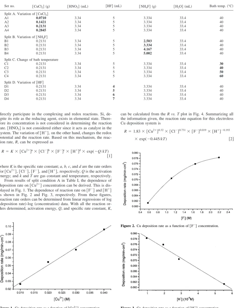
energy; and k and T are gas constant and temperature, respectively.From results of split condition A in Table I, the dependence of deposition rate on
关Cu
2⫹兴 concentration can be derived. This is dis-
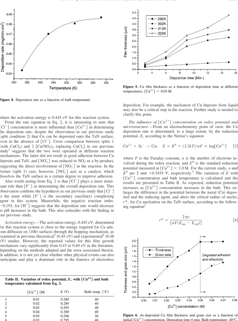
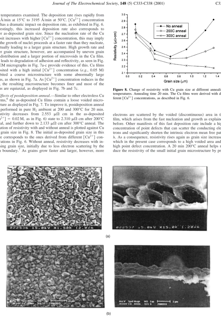
played in Fig. 1. The dependence of reaction rate on关F
⫺兴 and 关H
⫹兴
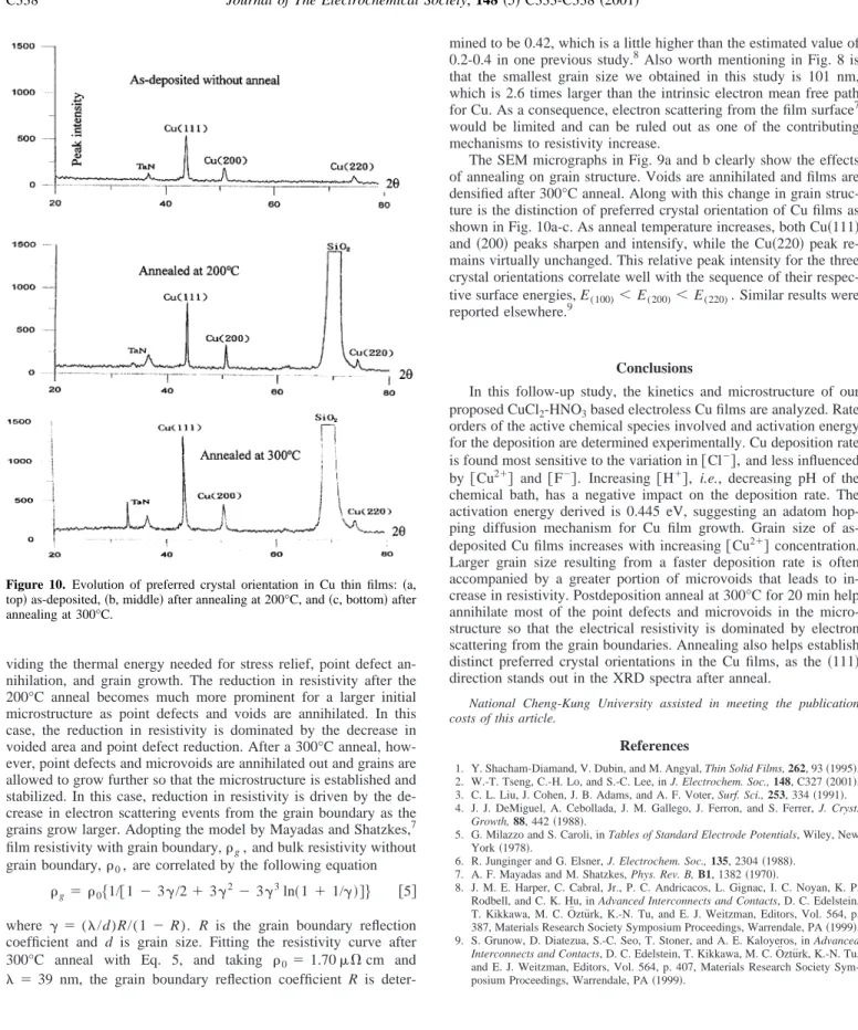
is shown in Fig. 2 and Fig. 3, respectively. From these figures, reaction rate orders can be determined from linear regressions of log共deposition rate兲-log 共concentration兲 data. With all the reaction or-
ders determined, activation energy, Q, and specific rate constant, K,can be calculated from the R vs. T plot in Fig. 4. Summarizing all the information given, the reaction rate equation for this electroless Cu deposition system is
R
⫽ 1.83 ⫻ 关Cu
2⫹兴
0.32⫻ 关Cl
⫺兴
0.731⫻ 关F
⫺兴
0.019⫻ 关H
⫹兴
⫺0.193⫻ exp共⫺0.445/kT兲 关2兴
Table I. Split conditions and parameters used for the determination of reaction kinetics.
Set no. 关CuCl2兴 共g兲 关HNO3兴 共mL兲 关HF兴 共mL兲 关NH4F兴 共g兲 关H2O兴 共mL兲 Bath temp.共°C兲
Split A. Variation of关CuCl2兴
A1 0.0710 3.34 5 3.334 33.4 40
A2 0.1421 3.34 5 3.334 33.4 40
A3 0.2131 3.34 5 3.334 33.4 40
A4 0.2845 3.34 5 3.334 33.4 40
Split B. Variation of关NH4F兴
B1 0.2131 3.34 5 2.503 33.4 40
B2 0.2131 3.34 5 3.334 33.4 40
B3 0.2131 3.34 5 4.167 33.4 40
B4 0.2131 3.34 5 5.002 33.4 40
Split C. Change of bath temperature
C1 0.2131 3.34 5 3.334 33.4 30
C2 0.2131 3.34 5 3.334 33.4 40
C3 0.2131 3.34 5 3.334 33.4 50
C4 0.2131 3.34 5 3.334 33.4 60
Split D. Variation of关HF兴
D1 0.2131 3.34 4 3.334 33.4 40
D2 0.2131 3.34 5 3.334 33.4 40
D3 0.2131 3.34 6 3.334 33.4 40
D4 0.2131 3.34 7 3.334 33.4 40
Figure 1. Cu deposition rate as a function of关Cu2⫹兴 concentration.
Figure 2. Cu deposition rate as a function of关F⫺兴 concentration.
Figure 3. Cu deposition rate as a function of关H⫹兴 concentration.
where the activation energy is 0.445 eV for this reaction system.
From the rate equation in Eq. 2, it is interesting to note that
关Cl
⫺兴 concentration is more influential than 关Cu
2⫹兴 in determining
the deposition rate, despite the observation in our previous study共split condition 2兲 that Cu can be deposited onto the TaN surface,
even in the absence of关Cl
⫺兴. Cross comparison between splits 1 共with CuCl
2兲 and 2 关Cu共NO
3兲
2 replacing CuCl2兴 in our previous
study2 suggests that the two were operated at different reaction mechanisms. The latter did not result in good adhesion between Cu deposits and TaN, and关NO
3⫺兴 was reduced to NO
2as a by-product, suggesting the direct involvement of关NO
3⫺兴 in the reaction. In the
former共split 1兲 case, however, 关NO
3⫺兴 acts as a catalyst, which
dissolves the TaN surface to a certain degree to improve adhesion.Also worth noting from Eq. 2 is that
关Cl
⫺兴 plays a more domi-
nant role than关F
⫺兴 in determining the overall deposition rate. This
observation confirms the hypothesis in our previous study that关Cl
⫺兴
is the main while关F
⫺兴 is the secondary 共auxiliary兲 complexing
agent in this system. Meanwhile, the negative reaction order,⫺0.193, for 关H
⫹兴 suggests that the deposition rate would decrease
as pH increases in the bath. This also coincides with the finding in our previous study.Activation energy.—The activation energy, 0.445 eV, determined for this reaction system is close to the energy required for Cu ada- tom diffusion on
共100兲 surfaces through the hopping mechanism, as
examined in previous theoretical3共0.45 eV兲 and experimental
4共0.48
eV兲 studies. However, the reported values for this film growth
mechanism vary significantly from 0.43 to 0.69 eV in the literature, depending on the methods adopted and the error associated therein.In addition, it is not yet clear whether other physical events can also participate and play a dominant role in the kinetics of electroless
deposition. For example, the nucleation of Cu deposits from liquid may also be a critical step in the reaction. Further study is needed to clarify this point.
The influence of
关Cu
2⫹兴 concentration on redox potential and
microstructure.—From an electrochemistry point of view, the Cu deposition rate is determined, to a large extent, by the reduction potential, E, according to the Nernst’s equationCu2⫹
⫹ 2e
⫺→ Cu; E ⫽ E0⫹ 共2.3kT兲/nF ⫻ log关Cu
2⫹兴 关3兴
where F is the Faraday constant, n is the number of electrons in- volved during the redox reaction, and E0is the standard reduction potential measured at
关Cu
2⫹兴 ⫽ 1.0 M. For the current study, n and
E0 are 2 and⫹0.3419 V, respectively.
5 The variation of E with关Cu
2⫹兴 concentration and bath temperature is calculated and the
results are presented in Table II. As expected, reduction potential increases as关Cu
2⫹兴 concentration increases in the bath. This en-
larges the difference in the potential between the metal共Cu兲 depos-
ited and the reducing agent, and alters the critical radius of nuclei, r*, for Cu nucleation on the TaN surface, according to the follow- ing equation2r*
⫽
2␥v
关nF共E
me⫺ E
red兲兴 关4兴
Figure 5. Cu film thickness as a function of deposition time at different temperatures.关Cu2⫹兴 ⫽ 0.03 M.
Figure 6. As-deposited Cu film thickness and grain size as a function of initial关Cu2⫹兴 concentration. Deposition time 6 min. Bath temperature: 40°C.
Film adhesion and reflectivity started to degrade when关Cu2⫹兴 concentration exceeds 0.05 M.
Table II. Variation of redox potential, E, with†Cu2¿‡ and bath temperature calculated from Eq. 3.
关Cu2⫹兴 共M兲 E共V兲 Bath temp.共°C兲
1 0.01 0.280 40
2 0.02 0.289 40
3 0.03 0.295 40
4 0.04 0.300 40
5 0.03 0.296 30
6 0.03 0.295 40
7 0.03 0.293 50
8 0.03 0.290 60
Figure 4. Deposition rate as a function of bath temperature.
where
␥ is the surface tension, v is the molar volume of the metal
deposit, n is the number of electrons involved in the redox reaction, F is the Faraday constant, and (Eme⫺ E
red) is the potential between the metal共Cu兲 deposited and reducing agent. As the potential dif-
ference, (Eme⫺ E
red), increases in the solution r* becomes smaller, leading to an enhanced nucleation rate on TaN surface. A direct result of this is the increase in deposition rate. Also shown in Table II is that the reduction potential for关Cu
2⫹兴 decreases as tem-
perature rises. At the same time, the potential for reductant, Ered, also decreases. As a consequence, (Eme
⫺ E
red) and hence the nucleation rate does not change much. Raising the bath temperature, however, does provide more thermal energy for nuclei to grow and leads to larger grains, as shown later.The deposited Cu film thickness is plotted against deposition time in Fig. 5 at four different temperatures. As can be observed clearly, after 3 min, a stable deposition rate can be maintained for all Figure 7. Top view and cross-sectional views of the Cu microstructures deposited at different关Cu2⫹兴 concentrations: 关Cu2⫹兴 ⫽ 共a, top兲 0.05, 共b, middle兲 0.03, and共c, bottom兲 0.01 M. Bath temperature held at 40°C in all three cases.
four temperatures examined. The deposition rate rises rapidly from 374 Å/min at 15°C to 3195 Å/min at 50°C.
关Cu
2⫹兴 concentration
also has a dramatic impact on deposition rate, as exhibited in Fig. 6.Interestingly, this increased deposition rate also corresponds to larger as-deposited grain size. Since the nucleation rate of the Cu deposit increases with higher
关Cu
2⫹兴 concentration, this may imply
that the growth of nuclei proceeds at a faster rate than they nucleate, eventually leading to a larger grain structure. High growth rate and larger grain structure, however, are accompanied by uneven grain size distribution and a larger portion of microvoids in the Cu film.This leads to degradation of adhesion and reflectivity, as seen in Fig.
6. SEM micrographs in Fig. 7a-c provide evidence of this. Cu films deposited with a high initial
关Cu
2⫹兴 concentration 共e.g., 0.05 M兲
exhibited a course microstructure with some abnormally large grains, as shown in Fig. 7a. As关Cu
2⫹兴 concentration reduces in the
bath, the resulting microstructure becomes finer and most of the grains are equiaxial, as displayed in Fig. 7b and 7c.Effects of postdeposition anneal.—Similar to other electroless Cu systems,6the as-deposited Cu films contain a loose voided micro- structure as displayed in Fig. 7. To improve it, postdeposition anneal was performed in pure H2ambient at 200 and 300°C for 20 min.
Resistivity decreases from 2.553
⍀ cm in the as-deposited
(关Cu
2⫹兴 ⫽ 0.02 M, as in Fig. 6兲 state to 2.310 ⍀ cm after 200°C
anneal, and further down to 2.133⍀ cm after 300°C anneal. The
evolution of resistivity with and without anneal is plotted against Cu film grain size in Fig. 8. The initial as-deposited grain size in this figure corresponds to the ones derived from different关Cu
2⫹兴 con-
centrations in Fig. 6. Without anneal, resistivity decreases with in- creasing grain size, initially due to less electron scattering by the grain boundary.7As grains grow faster and larger, however, moreelectrons are scattered by the voided
共discontinuous兲 area in the
film, which arises from the fast nucleation and growth as explained before. Other manifests of this fast deposition rate include a high concentration of point defects that can scatter the conducting elec- trons and significantly shorten the intrinsic electron mean free path,. As a consequence, resistivity rises again as grain size increases,
which in the present case corresponds to a high voided area and a high point defect concentration. A 20 min 200°C anneal helps re- duce the resistivity of the small initial grain microstructure by pro-Figure 9. SEM micrographs showing grain structure共a兲 before annealing and 共b兲 after a 20 min 200°C anneal.
Figure 8. Change of resistivity with Cu grain size at different annealing temperatures. Annealing time 20 min. The Cu films were derived with dif- ferent关Cu2⫹兴 concentrations, as described in Fig. 6.
viding the thermal energy needed for stress relief, point defect an- nihilation, and grain growth. The reduction in resistivity after the 200°C anneal becomes much more prominent for a larger initial microstructure as point defects and voids are annihilated. In this case, the reduction in resistivity is dominated by the decrease in voided area and point defect reduction. After a 300°C anneal, how- ever, point defects and microvoids are annihilated out and grains are allowed to grow further so that the microstructure is established and stabilized. In this case, reduction in resistivity is driven by the de- crease in electron scattering events from the grain boundary as the grains grow larger. Adopting the model by Mayadas and Shatzkes,7 film resistivity with grain boundary,
g, and bulk resistivity without grain boundary,
0, are correlated by the following equation
g⫽
0兵1/关1 ⫺ 3␥/2 ⫹ 3␥
2⫺ 3␥
3ln共1 ⫹ 1/␥兲兴
其关5兴
where␥ ⫽ (/d)R/(1 ⫺ R). R is the grain boundary reflection
coefficient and d is grain size. Fitting the resistivity curve after 300°C anneal with Eq. 5, and taking
0⫽ 1.70 ⍀ cm and
⫽ 39 nm, the grain boundary reflection coefficient R is deter-
mined to be 0.42, which is a little higher than the estimated value of 0.2-0.4 in one previous study.8Also worth mentioning in Fig. 8 is that the smallest grain size we obtained in this study is 101 nm, which is 2.6 times larger than the intrinsic electron mean free path for Cu. As a consequence, electron scattering from the film surface7 would be limited and can be ruled out as one of the contributing mechanisms to resistivity increase.
The SEM micrographs in Fig. 9a and b clearly show the effects of annealing on grain structure. Voids are annihilated and films are densified after 300°C anneal. Along with this change in grain struc- ture is the distinction of preferred crystal orientation of Cu films as shown in Fig. 10a-c. As anneal temperature increases, both Cu
共111兲
and共200兲 peaks sharpen and intensify, while the Cu共220兲 peak re-
mains virtually unchanged. This relative peak intensity for the three crystal orientations correlate well with the sequence of their respec- tive surface energies, E(100)⬍ E
(200)⬍ E
(220). Similar results were reported elsewhere.9Conclusions
In this follow-up study, the kinetics and microstructure of our proposed CuCl2-HNO3based electroless Cu films are analyzed. Rate orders of the active chemical species involved and activation energy for the deposition are determined experimentally. Cu deposition rate is found most sensitive to the variation in
关Cl
⫺兴, and less influenced
by关Cu
2⫹兴 and 关F
⫺兴. Increasing 关H
⫹兴, i.e., decreasing pH of the
chemical bath, has a negative impact on the deposition rate. The activation energy derived is 0.445 eV, suggesting an adatom hop- ping diffusion mechanism for Cu film growth. Grain size of as- deposited Cu films increases with increasing关Cu
2⫹兴 concentration.
Larger grain size resulting from a faster deposition rate is often accompanied by a greater portion of microvoids that leads to in- crease in resistivity. Postdeposition anneal at 300°C for 20 min help annihilate most of the point defects and microvoids in the micro- structure so that the electrical resistivity is dominated by electron scattering from the grain boundaries. Annealing also helps establish distinct preferred crystal orientations in the Cu films, as the
共111兲
direction stands out in the XRD spectra after anneal.National Cheng-Kung University assisted in meeting the publication costs of this article.
References
1. Y. Shacham-Diamand, V. Dubin, and M. Angyal, Thin Solid Films, 262, 93共1995兲.
2. W.-T. Tseng, C.-H. Lo, and S.-C. Lee, in J. Electrochem. Soc., 148, C327共2001兲.
3. C. L. Liu, J. Cohen, J. B. Adams, and A. F. Voter, Surf. Sci., 253, 334共1991兲.
4. J. J. DeMiguel, A. Cebollada, J. M. Gallego, J. Ferron, and S. Ferrer, J. Cryst.
Growth, 88, 442共1988兲.
5. G. Milazzo and S. Caroli, in Tables of Standard Electrode Potentials, Wiley, New York共1978兲.
6. R. Junginger and G. Elsner, J. Electrochem. Soc., 135, 2304共1988兲.
7. A. F. Mayadas and M. Shatzkes, Phys. Rev. B, B1, 1382共1970兲.
8. J. M. E. Harper, C. Cabral, Jr., P. C. Andricacos, L. Gignac, I. C. Noyan, K. P.
Rodbell, and C. K. Hu, in Advanced Interconnects and Contacts, D. C. Edelstein, T. Kikkawa, M. C. O¨ ztu¨rk, K.-N. Tu, and E. J. Weitzman, Editors, Vol. 564, p.
387, Materials Research Society Symposium Proceedings, Warrendale, PA共1999兲.
9. S. Grunow, D. Diatezua, S.-C. Seo, T. Stoner, and A. E. Kaloyeros, in Advanced Interconnects and Contacts, D. C. Edelstein, T. Kikkawa, M. C. O¨ ztu¨rk, K.-N. Tu, and E. J. Weitzman, Editors, Vol. 564, p. 407, Materials Research Society Sym- posium Proceedings, Warrendale, PA共1999兲.
Figure 10. Evolution of preferred crystal orientation in Cu thin films:共a, top兲 as-deposited, 共b, middle兲 after annealing at 200°C, and 共c, bottom兲 after annealing at 300°C.