Highly Selective Etching of GaAs on Al 0.2 Ga 0.8 As Using Citric Acid ÕH 2 O 2 ÕH 2 O Etching System
Chin-I. Liao, Mau-Phon Houng, and Yeong-Her Wang
zDepartment of Electrical Engineering, Institute of Microelectronics, National Cheng-Kung University, Tainan 701, Taiwan
Highly selective etching共⬎150兲 of GaAs over Al0.2Ga0.8As with low GaAs etch rates共⬍50 Å/s兲 can be performed using a newly developed CA/H2O2/H2O etchant (CA⫽ citric acid:H2O of 1:1 by weight兲. Modulating the H2O2content in this etching system can overcome the weakness of previously nonselective etching inference using CA/H2O2⫹ H2O, and solve the problem of excessive GaAs etch rates共⬎100 Å/s兲 associated with using traditional CA/H2O2solutions. When applied to pseudomorphic high electron mobility transistors 共PHEMTs兲, high etching uniformity and a smooth surface 共rms roughness of only 2.01 Å兲 are observed during gate recessing; the gate leakage currents are then suppressed, suggesting the applicability of the CA/H2O2/H2O system to fabricating PHEMTs.
© 2004 The Electrochemical Society. 关DOI: 10.1149/1.1803072兴 All rights reserved.
Manuscript submitted February 21, 2004; revised manuscript received March 29, 2004. Available electronically September 28, 2004.
Selective etching of GaAs over Al
xGa
1⫺xAs is a critical process in fabricating pseudomorphic high electron mobility transistors 共PHEMTs兲, heterojunction bipolar transistors, light emitting diodes, and lasers.
1,2Recently, selective reactive ion etching has been effec- tively applied to pattern small features due to the anisotropic nature and high selectivity.
3However, particularly in the gate recess pro- cess of PHEMTs, the ion-induced degradation of the 2D gas prop- erties cannot be wholly negligible.
4By comparison, the selective wet etching is simpler, lower in cost, and does not cause ion-induced damage.
Otsubo et al. first reported the use of the CA/H
2O
2etching sys- tem to etch GaAs materials.
5The system has been recently applied to selectively etch GaAs on Al
xGa
1⫺xAs.
6,7However, the selectivity is usually high when Al
xGa
1⫺xAs is used with x ⬎ 0.3, and declines seriously as the Al mole fraction decreases.
4,6-10A high Al concen- tration may raise issues of reliability associated with DX center traps.
11An Al mole fraction of ⬃20% is required to minimize this problem and ensure long-term stability.
A few researchers have realized high selectivity 共80-130兲 with a low Al fraction 共⬍0.22兲 by carefully controlling the volume ratio of citric acid/H
2O
2/NH
4OH or CA/H
2O
2.
12-14Nevertheless, the con- centration of hydrogen ions must be very accurately determined
12or the GaAs etch rate must be at least 110 Å/s to ensure high selectivity.
13,14However, such a high GaAs etch rate 共⬎100 Å/s兲 is undesirable because it does not allow the etch depth to be effectively controlled and causes excessive lateral etching, increasing the source resistance and degrading the device performance. Mao et al.
attempted to solve this problem by diluting the CA/H
2O
2with deionized 共DI兲 water.15Unfortunately, the GaAs etch rate truly de- clined but the selectivity completely disappeared. Accordingly, the etchant was concluded to be nonselective etching when the CA/H
2O
2⫹ H
2O system is used.
This work develops an effective method and advanced etching model to realize a highly selective etching in CA/H
2O
2/H
2O sys- tem. By considering the role of H
2O
2, it enables a low GaAs etch rate 共⬍50 Å/s兲 and high selectivity 共⬎150兲 to be achieved simulta- neously. The etching mechanism and its application to the PHEMT process are also discussed.
Experimental
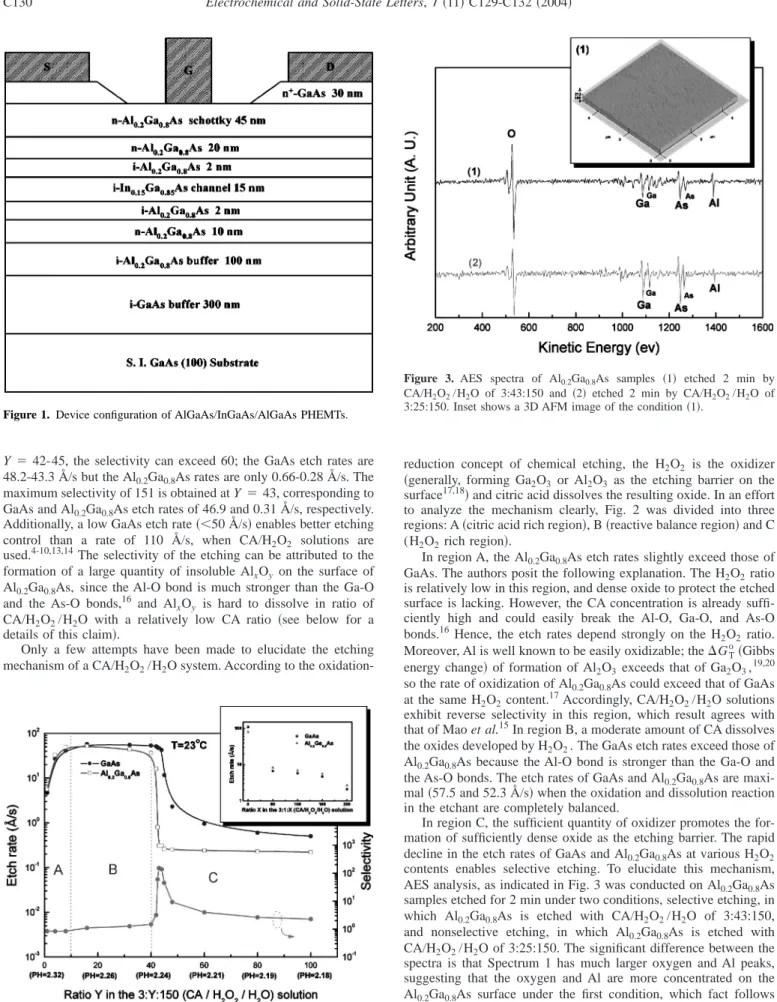
Epitaxial samples were all grown on semi-insulating GaAs 共100兲 substrates by molecular beam epitaxy. The GaAs and Al
0.2Ga
0.8As samples with Si-doped of 2 ⫻ 1018cm
⫺3were used for etch rates and selectivity measurements. The PHEMT structure, shown in
Fig. 1, consists of an In
0.15Ga
0.85As active channel layer sandwiched between two Al
0.2Ga
0.8As layers, as well as a heavily doped GaAs cap layer grown on the top of an Al
0.2Ga
0.8As barrier layer for good Ohmic contact.
In preparing CA/H
2O
2/H
2O solutions, the citric acid liquor 共CA兲 was first made by mixing 1:1 共by weight兲 citric acid 共monohydrate兲 with DI water at least one day in advance to ensure complete disso- lution. Then, the CA was freshly mixed with H
2O
2共31%兲 and DI water at a given volume ratio. The GaAs and Al0.2Ga
0.8As samples were simultaneously etched using the CA/H
2O
2/H
2O solution for a set time with stirring to examine the etch rates and selective etching.
The etching time was varied from 2 min to 2h, according to the material etch rates. Etching was terminated by rinsing in DI water for 1 min. The etch depth was measured using a Veeco Instrument DEKTAK after the photoresist mask was removed. The depth was determined at least six times with a deviation of 10 Å, indicating high reproducibility. The etch-stopping mechanism was elucidated using Auger electron spectroscopy 共AES兲 and the material surface quality was characterized by atomic force microscopy 共AFM兲.
In fabricating PHEMTs, an active layer was defined by wet etch- ing, followed by the evaporation of AuGe/Ni/Au and lift-off. Good Ohmic contacts were formed by annealing at 420°C for 30s. The gate recess was etched by a citric acid-based etchant. Then, the 1
⫻ 100 m gate pattern was defined and metalized with a Ti/Pt/Au metal stack.
Results and Discussion
The effect of diluting the CA/H
2O
2with DI water, on the etch rates of GaAs and Al
0.2Ga
0.8As, was examined and plotted in the inset of Fig. 2. The GaAs and Al
0.2Ga
0.8As etch rates were 110 and 80 Å/s, respectively, for a CA/H
2O
2ratio of 3:1. Clearly, the etch rates of both GaAs and Al
0.2Ga
0.8As declined as H
2O was added to CA/H
2O
2; also, the Al
0.2Ga
0.8As etch rate slightly exceeded that of the GaAs, which result agrees with the inference of nonselective etching in an earlier report.
15However, to the best of our knowledge, no report has investi- gated the participation of H
2O
2in this etching system. Figure 2 shows the etching model for the etch rates and the selectivity of GaAs and Al
0.2Ga
0.8As using various CA/H
2O
2/H
2O volume ratios of 3:Y :150. The hydrogen ion concentration is measured by an elec- tronic PH meter. For Y ⫽ 1-15, the etch rates of GaAs and Al
0.2Ga
0.8As strongly increase with the H
2O
2ratio, yielding a re- verse selectivity of 0.85. For Y ⫽ 16-40, the GaAs etch rates slightly exceed those of Al
0.2Ga
0.8As but none substantially vary for both of the etch rates. However, continuing to raise the H
2O
2ratio causes the GaAs and Al
0.2Ga
0.8As etch rates to fall rapidly at different H
2O
2ratios and then almost keep constant again. For
zE-mail: [email protected]
Electrochemical and Solid-State Letters, 7
共11兲 C129-C132 共2004兲
1099-0062/2004/7共11兲/C129/4/$7.00 © The Electrochemical Society, Inc.
C129
Downloaded 07 Sep 2008 to 140.116.208.41. Redistribution subject to ECS license or copyright; see http://www.ecsdl.org/terms_use.jsp
Y
⫽ 42-45, the selectivity can exceed 60; the GaAs etch rates are 48.2-43.3 Å/s but the Al0.2Ga
0.8As rates are only 0.66-0.28 Å/s. The maximum selectivity of 151 is obtained at Y ⫽ 43, corresponding to GaAs and Al
0.2Ga
0.8As etch rates of 46.9 and 0.31 Å/s, respectively.
Additionally, a low GaAs etch rate 共⬍50 Å/s兲 enables better etching control than a rate of 110 Å/s, when CA/H
2O
2solutions are used.
4-10,13,14The selectivity of the etching can be attributed to the formation of a large quantity of insoluble Al
xO
yon the surface of Al
0.2Ga
0.8As, since the Al-O bond is much stronger than the Ga-O and the As-O bonds,
16and Al
xO
yis hard to dissolve in ratio of CA/H
2O
2/H
2O with a relatively low CA ratio 共see below for a details of this claim 兲.
Only a few attempts have been made to elucidate the etching mechanism of a CA/H
2O
2/H
2O system. According to the oxidation-
reduction concept of chemical etching, the H
2O
2is the oxidizer 共generally, forming Ga2O
3 or Al
2O
3 as the etching barrier on the surface
17,18兲 and citric acid dissolves the resulting oxide. In an effort to analyze the mechanism clearly, Fig. 2 was divided into three regions: A 共citric acid rich region兲, B 共reactive balance region兲 and C (H
2O
2rich region 兲.
In region A, the Al
0.2Ga
0.8As etch rates slightly exceed those of GaAs. The authors posit the following explanation. The H
2O
2ratio is relatively low in this region, and dense oxide to protect the etched surface is lacking. However, the CA concentration is already suffi- ciently high and could easily break the Al-O, Ga-O, and As-O bonds.
16Hence, the etch rates depend strongly on the H
2O
2ratio.
Moreover, Al is well known to be easily oxidizable; the ⌬GT
o共Gibbs energy change 兲 of formation of Al
2O
3exceeds that of Ga
2O
3,
19,20
so the rate of oxidization of Al
0.2Ga
0.8As could exceed that of GaAs at the same H
2O
2content.
17Accordingly, CA/H
2O
2/H
2O solutions exhibit reverse selectivity in this region, which result agrees with that of Mao et al.
15In region B, a moderate amount of CA dissolves the oxides developed by H
2O
2. The GaAs etch rates exceed those of Al
0.2Ga
0.8As because the Al-O bond is stronger than the Ga-O and the As-O bonds. The etch rates of GaAs and Al
0.2Ga
0.8As are maxi- mal 共57.5 and 52.3 Å/s兲 when the oxidation and dissolution reaction in the etchant are completely balanced.
In region C, the sufficient quantity of oxidizer promotes the for- mation of sufficiently dense oxide as the etching barrier. The rapid decline in the etch rates of GaAs and Al
0.2Ga
0.8As at various H
2O
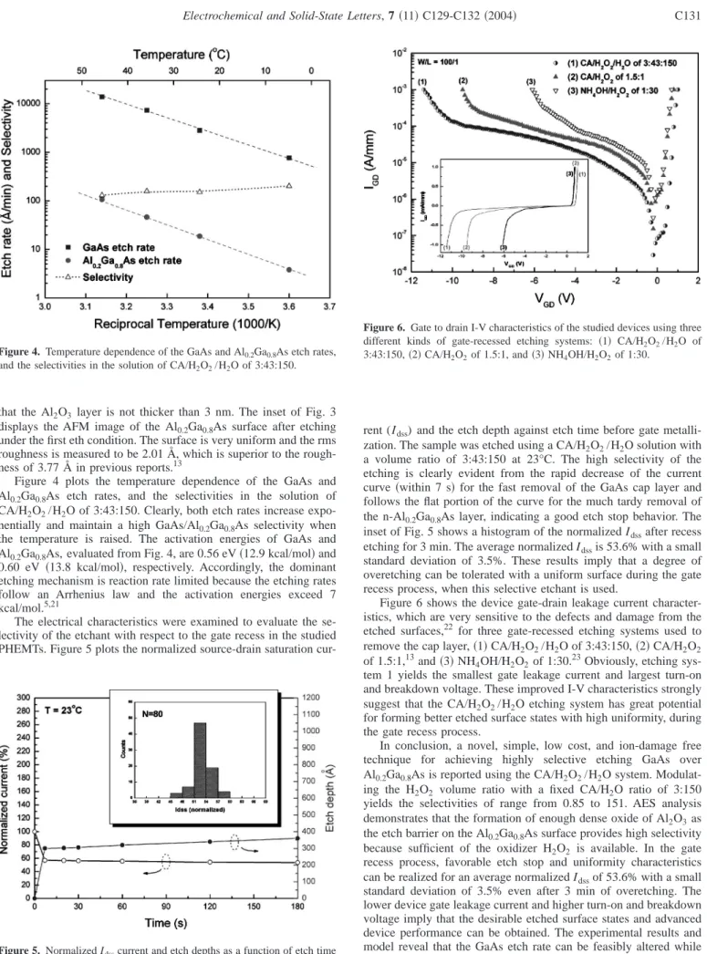
2contents enables selective etching. To elucidate this mechanism, AES analysis, as indicated in Fig. 3 was conducted on Al
0.2Ga
0.8As samples etched for 2 min under two conditions, selective etching, in which Al
0.2Ga
0.8As is etched with CA/H
2O
2/H
2O of 3:43:150, and nonselective etching, in which Al
0.2Ga
0.8As is etched with CA/H
2O
2/H
2O of 3:25:150. The significant difference between the spectra is that Spectrum 1 has much larger oxygen and Al peaks, suggesting that the oxygen and Al are more concentrated on the Al
0.2Ga
0.8As surface under the first condition, which fact follows from the formation of the Al
2O
3etch stop layer. The presence of the etch stop layer is further supported by the fact that the Ga and As peaks are lower than those in Spectrum 2. Auger electron escape depths are on the order of 2-3 nm, so the presence of the Ga and As peaks along with the oxygen and Al peaks in Spectrum 1 indicates
Figure 1. Device configuration of AlGaAs/InGaAs/AlGaAs PHEMTs.Figure 2. Inset shows the etch rates of GaAs and Al0.2Ga0.8As as a function of the volume ratio of CA/H2O2/H2O of 3:1:X. Main figure shows the etch rates of GaAs and Al0.2Ga0.8As, and the selectivity of GaAs/Al0.2Ga0.8As as a function of the CA/H2O2/H2O of 3:Y:150.
Figure 3. AES spectra of Al0.2Ga0.8As samples 共1兲 etched 2 min by CA/H2O2/H2O of 3:43:150 and 共2兲 etched 2 min by CA/H2O2/H2O of 3:25:150. Inset shows a 3D AFM image of the condition共1兲.
Electrochemical and Solid-State Letters, 7
共11兲 C129-C132 共2004兲 C130
Downloaded 07 Sep 2008 to 140.116.208.41. Redistribution subject to ECS license or copyright; see http://www.ecsdl.org/terms_use.jsp
that the Al
2O
3layer is not thicker than 3 nm. The inset of Fig. 3 displays the AFM image of the Al
0.2Ga
0.8As surface after etching under the first eth condition. The surface is very uniform and the rms roughness is measured to be 2.01 Å, which is superior to the rough- ness of 3.77 Å in previous reports.
13Figure 4 plots the temperature dependence of the GaAs and Al
0.2Ga
0.8As etch rates, and the selectivities in the solution of CA/H
2O
2/H
2O of 3:43:150. Clearly, both etch rates increase expo- nentially and maintain a high GaAs/Al
0.2Ga
0.8As selectivity when the temperature is raised. The activation energies of GaAs and Al
0.2Ga
0.8As, evaluated from Fig. 4, are 0.56 eV 共12.9 kcal/mol兲 and 0.60 eV 共13.8 kcal/mol兲, respectively. Accordingly, the dominant etching mechanism is reaction rate limited because the etching rates follow an Arrhenius law and the activation energies exceed 7 kcal/mol.
5,21The electrical characteristics were examined to evaluate the se- lectivity of the etchant with respect to the gate recess in the studied PHEMTs. Figure 5 plots the normalized source-drain saturation cur-
rent (I
dss) and the etch depth against etch time before gate metalli- zation. The sample was etched using a CA/H
2O
2/H
2O solution with a volume ratio of 3:43:150 at 23°C. The high selectivity of the etching is clearly evident from the rapid decrease of the current curve 共within 7 s兲 for the fast removal of the GaAs cap layer and follows the flat portion of the curve for the much tardy removal of the n-Al
0.2Ga
0.8As layer, indicating a good etch stop behavior. The inset of Fig. 5 shows a histogram of the normalized I
dssafter recess etching for 3 min. The average normalized I
dssis 53.6% with a small standard deviation of 3.5%. These results imply that a degree of overetching can be tolerated with a uniform surface during the gate recess process, when this selective etchant is used.
Figure 6 shows the device gate-drain leakage current character- istics, which are very sensitive to the defects and damage from the etched surfaces,
22for three gate-recessed etching systems used to remove the cap layer, 共1兲 CA/H2O
2/H
2O of 3:43:150, 共2兲 CA/H2O
2
of 1.5:1,
13and 共3兲 NH4OH/H
2O
2of 1:30.
23Obviously, etching sys- tem 1 yields the smallest gate leakage current and largest turn-on and breakdown voltage. These improved I-V characteristics strongly suggest that the CA/H
2O
2/H
2O etching system has great potential for forming better etched surface states with high uniformity, during the gate recess process.
O
2of 1.5:1,
13and 共3兲 NH4OH/H
2O
2of 1:30.
23Obviously, etching sys- tem 1 yields the smallest gate leakage current and largest turn-on and breakdown voltage. These improved I-V characteristics strongly suggest that the CA/H
2O
2/H
2O etching system has great potential for forming better etched surface states with high uniformity, during the gate recess process.
In conclusion, a novel, simple, low cost, and ion-damage free technique for achieving highly selective etching GaAs over Al
0.2Ga
0.8As is reported using the CA/H
2O
2/H
2O system. Modulat- ing the H
2O
2volume ratio with a fixed CA/H
2O ratio of 3:150 yields the selectivities of range from 0.85 to 151. AES analysis demonstrates that the formation of enough dense oxide of Al
2O
3as the etch barrier on the Al
0.2Ga
0.8As surface provides high selectivity because sufficient of the oxidizer H
2O
2is available. In the gate recess process, favorable etch stop and uniformity characteristics can be realized for an average normalized I
dssof 53.6% with a small standard deviation of 3.5% even after 3 min of overetching. The lower device gate leakage current and higher turn-on and breakdown voltage imply that the desirable etched surface states and advanced device performance can be obtained. The experimental results and model reveal that the GaAs etch rate can be feasibly altered while maintaining high selectivity, by appropriately setting the CA/H
2O
2/H
2O ratio, supporting the fabrication of a device with a heterostructure.
Figure 4. Temperature dependence of the GaAs and Al0.2Ga0.8As etch rates, and the selectivities in the solution of CA/H2O2/H2O of 3:43:150.
Figure 5. Normalized Idsscurrent and etch depths as a function of etch time for studied PHEMTs using a CA/H2O2/H2O of 3:43:150 solution. Inset shows the histogram of the normalized Idssafter recess etching for 3 min共80 specimens were examined for the 3 in. wafer with the probing system兲.
Figure 6. Gate to drain I-V characteristics of the studied devices using three different kinds of gate-recessed etching systems: 共1兲 CA/H2O2/H2O of 3:43:150,共2兲 CA/H2O2of 1.5:1, and共3兲 NH4OH/H2O2of 1:30.
Electrochemical and Solid-State Letters, 7
共11兲 C129-C132 共2004兲 C131
Downloaded 07 Sep 2008 to 140.116.208.41. Redistribution subject to ECS license or copyright; see http://www.ecsdl.org/terms_use.jsp
Acknowledgments
This work was supported in part by the National Science Council under contracts NSC92-2215-E006-008, NSC92-2215-E006-019, MOE Program for Promoting Academic Excellent of Universities under the grant no. A-91E-FA08-1-4 and the Foundation of Chen, Jieh-Chen scholarship 共Tainan, Taiwan兲.
National Cheng-Kung University assisted in meeting the publication costs of this article.
References
1. H. Wang and G. Ng, IEEE Electron Device Lett., 24, 628共2003兲.
2. R. Quay, K. Hess, R. Reuter, M. Schlechtweg, T. Grave, V. Palankovski, and S.
Selberherr, IEEE Trans. Electron Devices, 48, 210共2001兲.
3. E. Murakami, T. Yoshimura, Y. Goto, and S. Kimura, IEEE Trans. Electron De- vices, 47, 835共2000兲.
4. M. Tong, D. G. Ballegeer, A. Ketterson, E. J. Roan, K. Y. Cheng, and I. Adesida, J.
Electron. Mater., 21, 9共1992兲.
5. M. Otsubo, T. Oda, H. Kumabe, and H. Miki, J. Electrochem. Soc., 123, 676 共1976兲.
6. S. K. Cheong, B. A. Bunker, T. Shibata, D. C. Hall, C. B. DeMelo, Y. Luo, G. L.
Snider, G. Kramer, and N. El-Zein, Appl. Phys. Lett., 78, 2458共2001兲.
7. J. H. Kim, D. H. Lim, and G. M. Yang, J. Vac. Sci. Technol. B, 16, 558共1998兲.
8. C. Juang, K. J. Kuhn, and R. B. Darling, J. Vac. Sci. Technol. B, 8, 1122共1990兲.
9. F. Sfigakis, P. Paddon, V. Pacradouni, M. Adamcyk, C. Nicoll, A. R. Cowan, T.
Tiedje, and J. F. Young, J. Lightwave Technol., 18, 199共2000兲.
10. G. C. Desalvo, W. F. Tseng, and J. Comas, J. Electrochem. Soc., 139, 831共1992兲.
11. R. E. Leoni, J. Bao, J. Bu, X. Du, M. S. Shirokov, and J. C. M. Hwang, IEEE Trans. Electron Devices, 47, 498共2000兲.
12. T. Kitano, S. Izumi, H. Minami, T. Ishikawa, K. Sato, T. Sonoda, and M. Otsubo, J. Vac. Sci. Technol. B, 15, 167共1997兲.
13. E. A. Moon, J. J. Lee, and H. M. Yoo, J. Appl. Phys., 84, 3933共1998兲.
14. H. J. Lee, M. S. Tae, K. Radhakrishnan, K. Prasad, J. Weng, S. F. Yoon, X. Zhou, H. S. Tan, S. K. Ting, and Y. C. Leong, Mater. Sci. Eng., B, 35, 230共1995兲.
15. B. Y. Mao, J. A. Nielsen, R. A. Friedman, and G. Y. Lee, J. Electrochem. Soc., 141, 1082共1994兲.
16. D. Briggs and M. P. Seah, Practical Surface Analysis, p. 602, John Wiley & Sons, New York共1990兲.
17. C. I. H. Ashby, J. P. Sullivan, K. D. Choquette, K. M. Geib, and H. Q. Hou, J. Appl.
Phys., 82, 3134共1997兲.
18. J. D. Kubicki and S. E. Apitz, Am. Mineral., 83, 1054共1998兲.
19. O. Kubaschewski, C. B. Alcock, and P. J. Spencer, Materials Thermochemistry, p.
6, Pergamon, New York共1993兲.
20. Y. Arai and D. L. Sparks, Soil Sci., 167, 303共2002兲.
21. B. Tuck, J. Mater. Sci., 10, 321共1975兲.
22. A. Nagayama, S. Yamauchi, and T. Hariu, IEEE Trans. Electron Devices, 47, 517 共2000兲.
23. R. P. Ribas, J. L. Leclercq, J. M. Karam, B. Courtois, and P. Viktorovitch, Mater.
Sci. Eng., B, 51, 267共1998兲.
Electrochemical and Solid-State Letters, 7
共11兲 C129-C132 共2004兲 C132
Downloaded 07 Sep 2008 to 140.116.208.41. Redistribution subject to ECS license or copyright; see http://www.ecsdl.org/terms_use.jsp