國立台灣大學電機資訊學院電子工程學研究所 碩士論文
Graduate Institute of Electronics Engineering College of Electrical Engineering & Computer Science
National Taiwan University Master Thesis
以氣態源分子束磊晶法成長砷化鎵於奈米矽溝渠之光 學特性
Optical Properties of GaAs in Si nano-trench grown by Gas Source Molecular Beam Epitaxay
胡哲寧 Che-Ning Hu
指導教授:林浩雄博士 Advisor: Hao-Hsiung Lin, Ph. D.
中華民國 100 年 7 月
July 2011
中文摘要 中文摘要 中文摘要 中文摘要
我們利用掃描式電子顯微鏡(SEM)、陰極螢光(CL)及拉曼(Raman)光譜量測以 氣態源分子束磊晶法成長在平面矽基板及有圖樣的矽基板上的砷化鎵。
從 SEM 的觀測,我們可以看到 300 奈米厚的砷化鎵成長於平面矽基板時,呈 現連續山狀的樣貌,並且有<100>方向的小縫隙分佈其間,砷化鎵的覆蓋率超過 95
%。而成長於有圖樣的矽機板的砷化鎵,幾乎全部都長入矽奈米溝渠中,藉由氫 等離子體的幫助,成功地達成選擇性成長,在溝渠寬度小於 200 奈米之後,才有 眼形的小塊堆積在溝渠邊緣的二氧化矽上。
砷化鎵成長於平面矽基板及成長於奈米矽溝渠內的室溫(RT)和低溫(LT)的 CL 光譜也被量測。無論是成長於平面矽基板還是成長於奈米矽溝渠內,室溫陰極螢 光的波峰相較於同質磊晶的砷化鎵皆呈現相同程度約三倍的變寬,以及 30 meV 左 右的藍移。我們認為波峰變寬主要歸因於各個被拉張或擠壓的結晶為了達到費米 能階一致而造成的能帶變形,以致於原有的能階數減少,在電子束產生大量載子 的同時,也同時填滿能階到更高/低能階,造成放光時波峰的變寬。而大程度的藍 移則歸咎於成長時的自動摻雜,或所謂的 Burstein-Moss shift。成長於矽奈米溝 渠內的砷化鎵 LTCL 光譜在溝渠寬度介於 90 奈米至 140 奈米間的波形呈現雙峰態。
較低能量的波段被歸因於深層載子與碳受體的復合,而較高能量的波段則被歸因 於施體與受體的復合。在溝渠寬度大於 140 奈米之後,其放光波形接近成長於平 面矽機板的砷化鎵,藉由高斯(Gaussian)分佈擬合波峰,可以得到三至四個波峰。
而溝渠邊緣的二氧化矽由於缺陷結構放光,共有三個波段。常溫時為 1.9 eV 的放 光,歸因於非橋接氧電洞中心;2.2 eV 的放光,歸因於氧空洞與空隙氧分子間電 子電洞的復合;2.7 eV 的放光,歸因於矽孤對電子與電洞的復合。在 LTCL 的觀察 中,2.2 eV 及 2.7 eV 這兩種放光會縮減,起因於降溫時對這兩種缺陷結構的消減。
常溫的拉曼光譜也觀察到不尋常的現象:在所有的試片中我們均量測到強烈
的原本禁帶的橫向聲子模態。我們認為此一現象是源於晶體中大量的微雙晶缺 陷,此種缺陷會把原本(001)面轉成{122}面。另一現象是在溝渠寬度小於 100 nm 以後,我們使用 Lorentz 分佈擬合的實驗值在橫向聲子與縱向聲子模態之間有多 一「表面聲子」模態,起因於較大的表面積/體積比。
Abstract
We have utilized scanning electron microscopy (SEM), cathodoluminescence (CL)
spectroscopy and Raman spectroscopy to investigate heteroepitaxial GaAs on planar Si
and patterned Si wafer samples grown by gas source molecular beam epitaxy (GSMBE)
system.
With the observation of SEM image of the sample top view, the hydrogen-plasma
-assisted-grown-300-nm-thick-GaAs on Si planar substrate formed a successional
mountain-like “perforated film”. This structure composed by GaAs covers more than
95% area of the planar Si substrate. The filling ratio of GaAs in the trenches is
estimated to be nearly 100%. GaAs in the trenches break to become nanowires with
lengths varying from hundreds nanometer to several micron. When the trench widths
decrease less than 200 nm, the epi-GaAs overflow the trench onto the SiO2 sidewall and
form eye-shaped islands whose dimension is about 500 nm.
Room temperature CL (RTCL) and low temperature CL (LTCL) are also performed
at trenches whose widths vary from 50 nm to 500 nm. The RTCL GaAs peaks of all
trenches are about 3 times broadened and the same blue shifted about 30 meV
regardless of the trench width. Meanwhile, the energies of SiO2 peaks remain
unchanged. This phenomenon indicates that the blue shift and the broadening are due to
the same mechanism. We attribute the blue shift to the Burstein-Moss shift. The
broadening is attributed to the Fermi-level-consistency of grains induced band banding.
The LTCL GaAs peaks reveal a two-peak feature when trench width between 90 nm and
140 nm. The low energy band is attributed to deep level carrier to carbon acceptor and
the high energy band is attributed to donor to acceptor recombination, respectively.
When trench width is larger than 140 nm, the peak form is like GaAs on planar (001) Si.
With the assistance of Gaussian fitting, there are three or four bands. The origins of
three SiO2 RTCL peaks are also surveyed. The 1.9 eV peak is attributed to the NBOHC;
the 2.2 eV peak is attributed to the (VO;(O2)i) structure and the 2.7 eV peak is attributed
to E’ center. From the observation of LTCL, we find out that the elimination of 2.7 eV
and 2.2 eV peaks, which represents the elimination of these defects
The RT Raman spectra of GaAs on planar Si (001) substrates are measured in
z(XX)z’ and z(xx)z’ configurations. Regardless of the growth condition, all samples
reveal a strong originally forbidden transverse optical (TO) phonon mode. The RT
Raman spectra of GaAs in variant trench widths are measured in z(YY)z’ configuration.
Each of the epi-GaAs in Si nanotrenches also reveals a strong TO phonon mode and the
longitudinal optical (LO) phonon mode broadens. Furthermore, there is an additional
peak between the TO and the LO peak while trench width is under 100 nm, which is
attributed to the surface optical (SO) phonon mode. The SO mode is measured because
of the large surface-to-volume ratio.
Contents
中文摘要...i
Abstract...iii
Contents...v
Table Captions...vi
Figure Captions...vii
Chapter 1 Introduction...1
Chapter 2 Patterned Si Substrate, Experimental Apparatus and Scanning Electron Microscopy (SEM) Observations 2.1 Patterned Si Substrate...4
2.2 Gas Source Molecular Beam Epitaxy………..4
2.3 Scanning Electron Microscopy and Cathodoluminescence……….…6
2.4 Micro Raman Spectroscopy………...8
2.5 SEM images of GaAs in trenches with variant widths………..10
Chapter 3 Cathodoluminescence of GaAs in Si Nanotrenches 3.1 Excitation Volume of Electron………..….28
3.2 CL spectrum analysis of SiO2 as the shallow trench isolation.…………... ...29
3.2.1 Typical CL spectrum of SiO2 as STI……….29
3.2.2.1 The red band (R-band) luminescence of 1.9 eV (645 nm)………..30
3.2.2.2 The 2.2 eV (560 nm) band………...30
3.2.2.3 The 2.7eV (460nm) band……….31
3.2.2.4 The reduction of 2.2eV and 2.7eV bands at low temperature (11K)………..31
3.3 Growth Condition of GaAs on planar and patterned Si (001) wafer…………...32
3.4 RTCL spectra of GaAs on bulk/patterned Si………...33
3.4.1 The RTCL peaks discussion of GaAs grown on planar Si (001) samples………..33
3.4.2 RTCL spectra of GaAs in patterned Si……….35
3.4.3 LTCL spectra discussion of C2588 bulk………...37
3.4.4 LTCL spectra discussion of patterned C2588………...38
Chapter 4 Raman Spectroscopy of GaAs in Si Nanotrenches 4.1 T64000 calibration……….52
4.2 C2584-C2587 on Si bulk………...52
4.3 C2588 GaAs on patterned Si substrate………..54
4.4 Theory of Raman scattering………...56
Chapter 5 Conclusion………68
Table Captions
Chapter 1
Table 1.1 Physical properties of Si、Ge and III-V semiconductors at 300K……….7
Chapter 3
Table 3.1 The growth condition of C2584, C2585, C2586, C2587 and C2588……….40
Figure Captions
Chapter 2
Figure 2.1 (a) SEM image of 55nm trench. (b) The schematic graph of the cross section
of the trenches………12
Figure 2.2 (a) The source assembly of Ga and As port in VG-V80H GSMBE. (b) The molecular beams were paralleled to the long side of the trenches…………13
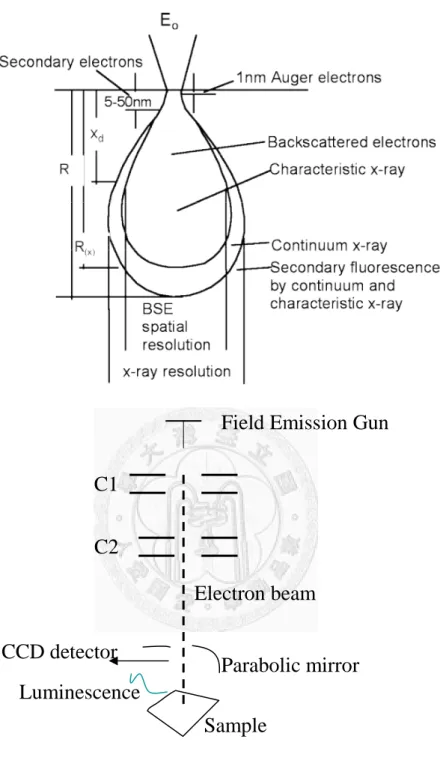
Figure 2.3 (a) The schematic graph of electron distribution, where Xd is the diffusion path and R the maximum range (b) The schematic graph of FEGSEM with CL system………..14
Figure 2.4 (a) Schematic graph of photon scattering (b) Schematic graph of the configuration of HORIBA Jobin-Yvon T64000 system………15
Figure 2.5 (a) VPEC GaAs room temperature CL with variant exposure time. (b) The laser polarization of T64000 is X direction. The incident direction is set to be z direction. (c) Different polarization of (001) VPEC GaAs Raman spectra………16
Figure 2.6 The SEM images of GaAs in 40 nm Si trenches………...17
Figure 2.7 The SEM images of GaAs in 55 nm Si trenches………...18
Figure 2.8 The SEM images of GaAs in 70 nm Si trenches………...19
Figure 2.9 The SEM images of GaAs in 80 nm Si trenches………...20
Figure 2.10 The SEM images of GaAs in 100 nm Si trenches………...21
Figure 2.11 The SEM images of GaAs in 120 nm Si trenches………...22
Figure 2.12 The SEM images of GaAs in 140 nm Si trenches………...23
Figure 2.13 The SEM images of GaAs in 160 nm Si trenches………...24
Figure 2.14 The SEM images of GaAs in 180 nm Si trenches……….………..25
Figure 2.15 The SEM images of GaAs in 200 nm Si trenches………...26
Figure 2.16 The SEM images of GaAs in 300 nm, 500 nm, 1 µm, 1.25 µm and 1.5 µm Si trenches………..27
Chapter 3
Figure 3.1 (a) The CL spectra of SiO2 STI side wall at RT using scan mode with variant exposure time The SEM images of GaAs in 200 nm Si trenches(b) A CL spectrum of SiO2 STI sidewall at 11K using spot mode (c) a CL spectrum of SiO2 as STI at 11K using spot mode……….41Figure 3.2 (a) RTCL of GaAs on GaAs substrate (b) LTCL of GaAs on GaAs substrate (c) C2585 SEM top view (d) C2586 SEM top view (e) C2588 SEM top view………...42
Figure 3.3 (a) RTCL of C2585 GaAs on planar Si (b) RTCL of C2586 GaAs on planar
Si (c) RTCL of C2588 GaAs on planar Si……….43
Figure 3.4 (a) RTCL of C2585 in 50 nm trench (b) RTCL of C2585 in 55 nm trench (c)
RTCL of C2585 in 60 nm trench (d) RTCL of C2585 in 70 nm trench…44
Figure 3.5 (a) RTCL of C2585 in 80 nm trench (b) RTCL of C2585 in 90 nm trench (c)
RTCL of C2585 in 100 nm trench (d) RTCL of C2585 in 120 nm
trench……….45
Figure 3.6 (a) RTCL of C2585 in 140 nm trench (b) RTCL of C2585 in 160 nm trench
(c) RTCL of C2585 in 180 nm trench (d) RTCL of C2585 in 200 nm
trench……….46
Figure 3.7 (a) RTCL of C2588 in 300nm trench (b) RTCL of C2588 in 500nm trench (c)
no beam emission spectrum (d) peaks positions by Gaussian fitting versus
trench widths………47
Figure 3.8 (a) RTCL spectrum of C2588 GaAs on planar Si with Gaussian fitting (b)-(d)
are LTCL spectra on the same spot, (e) (f) are on another spot, green curves
are the fitted Gaussian peaks………...48
Figure 3.9 C2588 variant trench width LTCL (a) 40 nm, (b) 55 nm, (c) 80 nm, (d) 90
nm (e) 100 nm, (f) 120 nm………..49
Figure 3.10 C2588 variant trench width LTCL (a) 140 nm (b) 160 nm (c) 180 nm (d)
200 nm (e) 300 nm (f) 500 nm………50
Figure 3.11 (a) LTCL Gaussian fitted C2588 GaAs on planar Si (001) substrate FWHM
versus peaks (b) LTCL Gaussian fitted C2588 GaAs on patterned Si (001)
substrate peak position versus trench width………..51
Chapter 4
Figure 4.1 (a) RT Raman spectrum of Si (100) bulk with z(XX)z’ configuration (b) RT
Raman spectrum of VPEC GaAs (100) with z(yX)z’ configuration (c) RT
Raman spectrum of C2584 (100) bulk with z(XX)z’ configuration (d) RT
Raman spectrum of C2584 (100) bulk with z(yX)z’ configuration (e) P. A.
Temple et al. [31]’s result………..59
Figure 4.2 (a) C2585(100) bulk z(XX)z’ 30 seconds 2 cycle in log scale (b) C2585 (100)
bulk z(yX)z’ 30 seconds 2 cycle in log scale (c) C2585(100) bulk z(XX)z’ 30
seconds 2 cycle GaAs signal in linear scale (d) C2585 (100) bulk z(yX)z’ 30
seconds 2 cycle GaAs signal in linear scale………..60
Figure 4.3 (a) RT Raman spectrum of C2586(100) bulk with z(XX)z’ configuration in
log scale (b) RT Raman spectrum of C2586 (100) bulk with z(yX)z’
configuration in log scale (c) RT Raman spectrum of C2586 (100) bulk with
z(XX)z’ configuration GaAs signal in linear scale (d) RT Raman spectrum of
C2586 (100) bulk with z(yX)z’ configuration GaAs signal in linear scale...61
Figure 4.4 (a) RT Raman spectrum of C2587 (100) bulk with z(XX)z’ configuration in
log scale (b) RT Raman spectrum of C2587 (100) bulk with z(yX)z’
configuration in log scale (c) RT Raman spectrum of C2587 (100) bulk with
z(XX)z’ configuration GaAs signal in linear scale (d) RT Raman spectrum of
C2587 (100) bulk with z(yX)z’ configuration GaAs signal in linear scale...62
Figure 4.5 (a) C2588 GaAs in 40nm trench Raman spectrum in linear scale with
Lorentzian fitting (b) C2588 GaAs in 45nm trench Raman spectrum in linear
scale with Lorentzian fitting (c) C2588 GaAs in 50nm trench Raman
spectrum in linear scale with Lorentzian fitting (d) C2588 GaAs in 55nm
trench Raman spectrum in linear scale with Lorentzian fitting……….63
Figure 4.6 (a) C2588 GaAs in 60nm trench Raman spectrum in linear scale with
Lorentzian fitting (b) C2588 GaAs in 70nm trench Raman spectrum in linear
scale with Lorentzian fitting (c) C2588 GaAs in 80nm trench Raman
spectrum in linear scale with Lorentzian fitting (d) C2588 GaAs in 90nm
trench Raman spectrum in linear scale with Lorentzian fitting……….64
Figure 4.7 (a) C2588 GaAs in 100nm trench Raman spectrum in linear scale with
Lorentzian fitting (b) C2588 GaAs in 120nm trench Raman spectrum in
linear scale with Lorentzian fitting (c) C2588 GaAs in 140nm trench Raman
spectrum in linear scale with Lorentzian fitting (d) C2588 GaAs in 160nm
trench Raman spectrum in linear scale with Lorentzian fitting……….65
Figure 4.8 (a) C2588 GaAs in 180nm Raman spectrum in linear scale with Lorentzian
fitting (b) C2588 GaAs in 200nm trench Raman spectrum in linear scale
with Lorentzian fitting (c) C2588 GaAs in 300nm trench Raman spectrum in
linear scale with Lorentzian fitting (d) C2588 GaAs in 500nm trench Raman
spectrum in linear scale with Lorentzian fitting………66
Figure 4.9 (a) The trends of TO phonon, SO phonon and LO phonon in variant trenches,
(b) The trends of FWHM of TO and LO phonon, respectively…………...67
Chapter 1 Introduction
From the 1980s, the properties of microns thick GaAs grown on Si and the
applications have been studied tremendously [1-6]. The superlattice method was used to
avoid the threading dislocation due to the 4% lattice mismatch [1-2]. The off cut little
angle along [100] of the Si (001) substrate provides the double step layer, which can
efficient avoid the anti phase boundary [3-4]. Low temperature photoluminescence
(LTPL) of GaAs on Si was measured and cross-section transmission electron
microscopy (TEM) was taken to observe the interface quality [5-6].
In the view of applications, since the invention of semiconductor transistor at 1947,
the booming of the Silicon based semiconductor industry has been commencing a
revolution of human livelihood. Forty six years ago, Moore [7] proposed a theory which
predicted a double of the number of transistors on chips every twelve months and later
refined the period to two years. Since then, the Moore’s law has kept going during the
past four decades by overcoming mountains of problems such as the limitation of
photolithography, high-k gate dielectric materials and strained-Si channel. However,
there exists a natural confinement: the size of a single transistor must lager than the Si
atom and the law will come to an end in the near future. In a tiny transistor, the
dominate feature is the driving current, which determine the speed of every single
transistor. While the current
( )
2= n2ox GS th
D V V
L W C
I µ , we spotlight on the mobility
enhancement in order to increase the gate current. High mobility materials such as GaAs,
InAs and Ge gained a lot of attentions and defect-free heteroepitaxial growth of these
materials becomes the research topic. Table 1.1 [1.8-9] shows the basic parameters of
these materials.
[8-9]
[9]
Chapter 2
Patterned Si Substrate, Experimental Apparatus and Scanning Electron Microscopy (SEM) Observations
2.1 Patterned Si Substrate
The patterned Si substrates used in this thesis were provided by Taiwan
Semiconductor Manufacturing Company (TSMC). Our goal is to selectively grow
high-quality GaAs and other relative III-V compound semiconductors, for example,
InAs, into the [1-10] direction trenches. The side walls are SiO2 of the trenches of the
shallow trench isolation (STI), which was fabricated on a (001) p-type Si substrate
using 193-nm immersion lithography and reactive ion etching (RIE) techniques. Figure
2.1 (a) and (b) show the SEM top view and the schematic cross-section graph of a
GaAs-grown trench, respectively. Table 2.1 lists the widths of all trenches, with length
of all trenches all the same about three millimeters and the same depth of 250nm.
2.2 Gas Source Molecular Beam Epitaxy
The specimens investigated in this thesis were grown by VG-V80H gas source
molecular beam epitaxy (GSMBE) system. The gallium cell and the arsenic cell
disposition were shown in Fig. 2.2(a). The gallium beam was supplied by EPI SUMO
cell and the arsenic dimmer beam for epitaxial growth was cracked from precursor
arsine at 1000 °C in a gas effusion cell. In addition to Ⅲ-Ⅴ sources, hydrogen plasma
species were generated by flowing H2 gas into EPI uni-bulb RF plasma cell operating at
13.56 MHz.
Before the epitaxial growth, both planar and nano-patterned Si substrates were
dipped in dilute HF solution (HF:H2O = 1:100) for 10 seconds to remove the native
oxide. After nitrogen blow drying, the chips were bonded onto molybdenum disk with
indium and inserted immediately into preparing chamber. The planar Si (001) substrate
was used to monitor the in-situ growth condition by Reflection high-energy electron
diffraction (RHEED) pattern. With the IRCON pyrometer monitoring the temperature,
the substrates were firstly heated up to 800 °C for 3 minutes to remove the residual
native oxide and the surface contaminations. After high temperature thermal cleaning,
the substrates temperature was cooled down to low temperature for subsequent epitaxial
growth.
During the epitaxial growth, the hydrogen plasma was always on until the end of
the growth to enhance the epitaxial selectivity [10]. In order to avoid shadowing effect,
the molecular beams was set parallel to the long side of the trenches as shown in figure
2.2(b). The growth temperature was set at 580 °C, and the deposition rate was 0.33
micron per hour, which was carefully calibrated on the Gallium beam flux using an ion
gauge. There were five periods of deposition, each growth 60 nanometer thick film and
than annealed at 640 °C for 10 minutes. After every period, the sample was rotated 180
degrees to enhance the epitaxial uniformity.
2.3 Scanning Electron Microscopy and Cathodoluminescence
SEM is a powerful tool to observe the surface appearance by using accelerated
electrons whose energy are thousands to tens of thousands electron volts as a light
source in optical microscopy. When the electrons hit into the sample, they diffuse and
scatter to a water-drop form distribution, providing Auger electron in the top 1nm range,
secondary electron in the top 5 to 50nm range, backscattered electrons, as shown in
figure 2.3 (a). With the detecting of secondary electrons, we can obtain the sample
appearance of a resolution up to 1nm.
Furthermore, the additional parts such as Auger electron spectrometer (AES),
electron energy loss spectrometer (EELS), and energy dispersive spectrometer (EDS)
can measure the chemical composition of samples; photoluminescence (PL), and
cathodoluminescence (CL) parts can measure the luminescence properties of samples to
receive detail information of the sample.
In CL measurements, a high energy electron beam whose energy was thousands
electron volts is utilized as an exciting source. Compared to the conventional PL
technique, CL measurement can provide higher spatial resolution, and with the in situ
SEM images, one can obtain the luminescence spectra at a precise position of the
sample, in our cases, i.e., the middle of the trench. Furthermore, the luminescence
images, or the chromatic CL mapping of samples, can be performed to analysis the
anti-phase boundaries and the non-radiation centers.
In this study, SEM images and CL spectrum were performed with JEOL JSM-7001
field emission gun SEM (FEGSEM). The SEM images were taken at a gun voltage of
8keV with a 12nA gun current and the CL spectra were taken at a gun voltage of 18keV
with a 16nA gun current, respectively. There are two modes to measure the CL
spectrum: scanning mode and spot mode. When using the scanning mode, the
magnification of SEM is fixed, and the luminescence signal contains the whole SEM
image range. On the other hand, when using the spot mode, the luminescence signals
are exactly produced from the spot we appointed about a range of several microns,
regardless of the magnification. The CL signals coming out from the samples are
reflected by a parabolic mirror into Horiba Jobin Yvon iHR550 spectrometer with
1200gr/mm grating through a 2000µm slit. After the signal collection and dispersion,
the final spectrum is obtained by a 1024x 256 pixel Si CCD detector with liquid
nitrogen cooling. A schematic graph of the apparatus is shown in figure 2.3 (b).
The spectra have a resolution about 0.03nm. In all cases, the raw data includes a
white noise about one thousand counts over entire spectrum. Besides, the data points
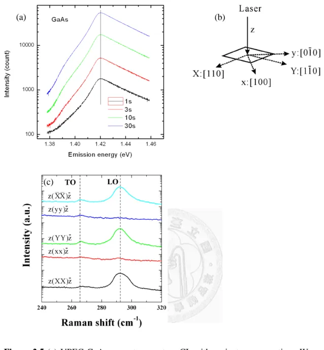
slightly zigzag everywhere. Figure 2.5 (a) is the room temperature (RT) CL spectra of
VPEC heteroepitaxial high purity GaAs with variant exposure time. We can see the
peak intensities are proportional to the exposure time, which represents that the high
energetic electrons bombardment does not influence the luminescence mechanism.
2.4 Micro Raman Spectroscopy
When a monochromatic light beam incident to a material, it would be scattered
elastically or inelastically. The elastically scattering is known as Rayleigh scattering and
inelastically scattering is known as Raman scattering. The Raman scattering was first
introduced by C. V. Raman and K. S. Krishnan at 1928 in liquid [11]. There are two
kinds of Raman scattering, providing a phonon referred as a Stokes scattering and
absorbing a phonon referred as an anti-Stokes scattering, respectively, as shown in
figure 2.15(a). The phenomenon can be expressed mathematically as:
Ω
±
=h h
hωs ωi (2.1)
q k kvs vi v
+
= (2.2)
where h the reduced Plank constant, ωi the angular frequency of incident light, ωs
the angular frequency of scattered light, Ω the angular frequency of phonon, ks v
the
momentum of scattered photon, ki v
the momentum of incident photon and qv the
momentum of phonon. Since the angular wavenumber of phonon (2π/a, where a is the
lattice constant) is much larger than photon (2π/λ, where λ is the wavelength of the
photon), the first order Raman scattering only accepts first Brillouin zone optical
phonon.
In this thesis, the properties of GaAs in single trench are of most interest. As a
result, we used HORIBA Jobin-Yvon T64000 system, a backscattering configuration
micro Raman system. The excitation light source is a 6 W Verdi V10 Diode-Pumped
Solid-State (DPSS) 532 nanometer Laser, which goes through two beam splitter and an
attenuator in order to make the beam power stable at 120 mW. Meanwhile, the laser
beam is focused to a 1 µm spot on the specimens by the 100X microscopic objective
lens. The backscattered light from the specimens transmit through a beam splitter and
enter into a triple monochromator, including a double premonochromator as a filter
stage and a single monochromator as a dispersive stage [12].
The filter stage has two gratings. First one disperses the incident light and second
one is coupled to the first one to collect the parallel light in order to diminish the
dispersion before light incident into the dispersive stage. There is a slit between the first
and the second grating. The size of slit and the dispersion power, DISP, of grating
decides the bandwidth and removes the stray light. The dispersive stage providing a
high level of stray light rejection and allow one to require low frequency Raman modes.
The dispersive stage with 1800gr/mm grating could disperse the inelastic Raman
scattering light and then the spectrum is collected by a 1024x 256 pixel Si CCD detector
with liquid nitride cooling. There are curtains around the system during experiment to
eliminate white noises.
Figure 2.5 (b) shows the incident laser beam polarization and the settled directions
and figure 2.5 (c) is the spectra of VPEC GaAs with different surface direction.
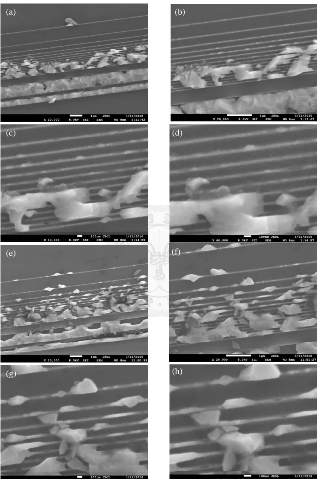
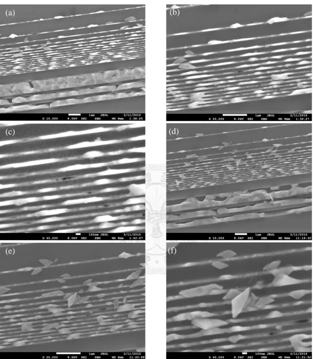
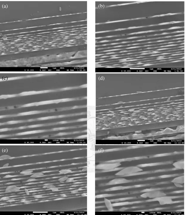
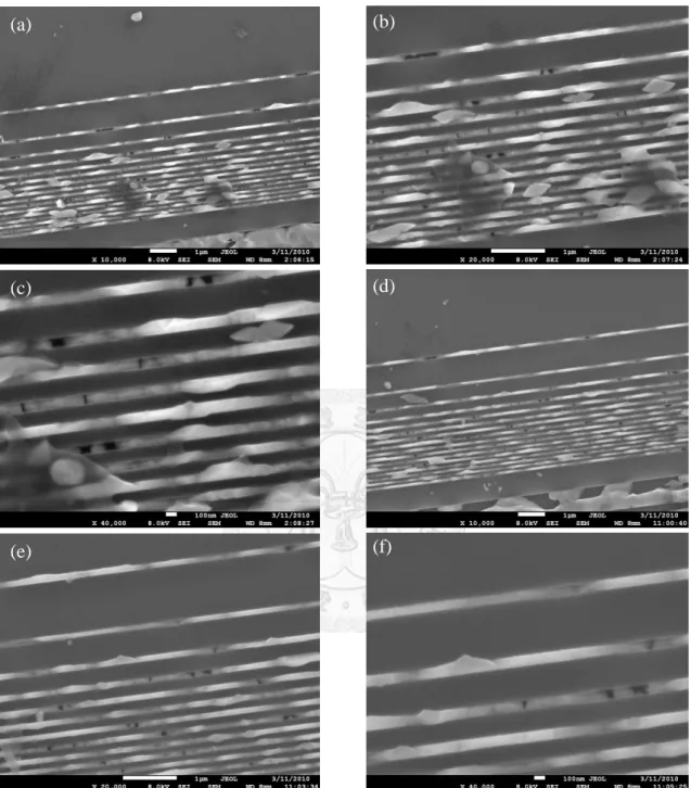
2.5 SEM images of GaAs in trenches with variant widths
The SEM images of GaAs in trenches with variant widths are shown in figure 2.6
to 2.14, with the orientation the same as figure 2.1. Through the investigation of SEM
images, we observed the filling rate is near hundred percent. In addition, there are
rhombic/eye-shaped GaAs islands above the STIs, with lengths about 1µm and widths
about 300nm, as a result of relatively low growth temperature compared to a previous
work presented by A. Okamoto et al. [13]. Inside the trenches, there are [110] direction
breakings between the GaAs bars and separate the entire GaAs bar in trenches into
several-microns-length bars. The breaking facets are all Si (1-10) facets. The heights of
the bars are not the same according to the contrast difference of the images.
Table 2.1 Different trench widths
number Trench width (nm)
5 40
6 45
7 50
8 55
9 60
10 70
11 80
12 90
13 100
14 120
15 140
16 160
17 180
18 200
19 300
20 500
Figure 2.1 (a) SEM image of 55nm trench, the lightest parts are the STI SiO2. Between
the STI are the trenches. There are 16 trenches at the upper side. The lowers are 1
micron, 500nm, and two 250nm trenches. (b) The schematic graph of the cross section
of the trenches. The side walls are amorphous silica and the bottom of trench are silicon.
Si
STI GaAs STI
[1-10]
[110]
[001]
SiO
2(a)
(b)
Figure 2.2 (a) The source assembly of Ga and As port in VG-V80H GSMBE. (b)
The molecular beams were paralleled to the long side of the trenches.
Group V cracking cell
Ga SUMO cell RF plasma cell
(b)
(a)
Figure 2.3 (a) The schematic graph of electron distribution, where Xd is the
diffusion path and R the maximum range (b) The schematic graph of FEGSEM
with CL system, where C1 and C2 are the electromagnetic lenses.
C1
Field Emission Gun
C2
Sample Electron beam
Luminescence
Parabolic mirror
(b)
Si CCD detector
(a)
Figure 2.4 (a) Schematic graph of photon scattering (b) Schematic graph of the
configuration of HORIBA Jobin-Yvon T64000 system
ω
ih
ω
i sh
h ω ω
is
h h ω
Ω
h h Ω
ω
sh
Rayleigh scattering anti-Stokes scattering Stokes scattering E
2E
1E
0(a)
(b)
Figure 2.5 (a) VPEC GaAs room temperature CL with variant exposure time. We can
see the peak intensity is proportional the exposure time, which means the high energy
16kV and 18nA electron gun does not influence the luminescence mechanism of GaAs.
(b) The laser polarization of T64000 is X direction. The incident direction is set to be z
direction. (c) Different polarization of (001) VPEC GaAs Raman spectra.
(a) (b)
(c)
Figure 2.6 The SEM images of GaAs in 40nm Si trenches: (a-d) middle of the trench long side with different magnification (e-h) right of the trench of the trench long side
(a) (b)
(c) (d)
(e) (f)
(g) (h)
Figure 2.7 The SEM images of GaAs in 55nm Si trenches: (a-d) middle of the trench long side with different magnification (e-h) right of the trench of the trench long side
(a) (b)
(c) (d)
(e) (f)
(g) (h)
Figure 2.8 The SEM images of GaAs in 70nm-wide Si trenches: (a-c) middle of the
trench long side with different magnification (d-f) right of the trench of the trench long
side with different magnification
(a) (b)
(c) (d)
(e) (f)
Figure 2.9 The SEM images of GaAs in 80nm-wide Si trenches: (a-c) middle of the
trench long side with different magnification (d-f) right of the trench of the trench long
side with different magnification
(a) (b)
(c) (d)
(e) (f)
Figure 2.10 The SEM images of GaAs in 100nm-wide Si trenches: (a-c) middle of the
trench long side with different magnification (d-f) right of the trench of the trench long
side with different magnification (a)
(e)
(b)
(c) (d)
(f)
Figure 2.11 The SEM images of GaAs in 120nm-wide Si trenches: (a-c) middle of the
trench long side with different magnification (d-f) right of the trench of the trench long
side with different magnification
(a) (b)
(c) (d)
(e) (f)
Figure 2.12 The SEM images of GaAs in 140nm-wide Si trenches: (a-b) middle of the
trench long side with different magnification (d-f) right of the trench of the trench long
side with different magnification
(a) (b)
(c) (d)
(e)
Figure 2.13 The SEM images of GaAs in 160nm-wide Si trenches: (a-b) middle of the
trench long side with different magnification (c-e) right of the trench of the trench long
side with different magnification
(a) (b)
(c) (d)
(e)
Figure 2.14 The SEM images of GaAs in 180nm-wide Si trenches: (a-b) middle of the
trench long side with different magnification (c-d) right of the trench of the trench long
side with different magnification
(a) (b)
(c) (d)
Figure 2.15 The SEM images of GaAs in 200nm-wide Si trenches: (a-b) middle of the
trench long side with different magnification (c-d) right of the trench of the trench long
side with different magnification
(a) (b)
(c) (d)
Figure 2.16 The SEM images of GaAs in (a-b) 300nm-wide trenches: middle of the
trench long side with different magnification (c) 500nm-wide trenches (d) 1µm-wide
trenches (e) 1.25µm-wide trenches (f) 1.5µm-width trenches
(a) (b)
(c) (d)
(e) (f)
Chapter 3
Cathodoluminescence of GaAs in Si Nanotrenches
3.1 Excitation Volume of Electron
As shown in figure 2.3 (a), when the electrons incident into a solid, the electron
diffuse to a water-drop shape distribution. The max penetration distance according to K.
Kanaya et al. [14] found to agree well with experimental results in a wider range of
atomic numbers [15] is
(
0.0276 /) ( )
µm= 0.889 b1.67
K A ρZ E
R (3.1)
, where A is the atomic weight in g/mol, ρ is the density in g/cm3, Z is the atomic
number and Eb is the electron energy in keV.
In our cases, setting Eb to 16 keV as we used in CL spectrum measurements, for
GaAs, A to 144.65, ρ to 5.316 , Z to 64, RKGaAs is 1.909µm, respectively. Furthermore,
for Si, we can substitute A to 28.0855, ρ to 2.329, Z to 14, R is 3.257µm, KSi
respectively, and for SiO2, we can substitute A to 60.08, ρ to 2.648, Z to 30, RKSiO2 is
3.122µm, respectively. All the data of densities, atomic weights and atomic numbers
used above are based on Wikipedia. According to these theoretical estimations, the
accelerated electrons would diffuse about 3 microns deep at the set point with a
water-drop form. Finally, since GaAs is only about 300 nm thick on or in the planar Si
or patterned Si substrates, the effective diffusion diameter at the bottom of GaAs is
estimated to be 2.6 µm.
3.2 CL spectrum analysis of SiO
2as the shallow trench isolation
3.2.1 Typical CL spectrum of SiO2 as STI
Figure 3.1(a) shows typical CL spectra of STI measured by scan mode. We can see
that there three bands, which are located at 1.9eV (645 nm), 2.2eV (560 nm) and 2.7eV
(460 nm), respectively. It is worth to mention that the intensity of these three peaks is
proportional to exposure time, as shown in Fig.3.1 (a), indicating that the 18
keV-energetic electrons bombardment does not influence the luminescence mechanism.
Figure 3.1(b) and (c) show the CL spectra measured by spot mode at 11K from the
side and the bottom of the trench, respectively. We can see both of the spectra are
almost the same. Since the trench width is 1µm, implying the electron dispersion range
much lager than 1 µm, as we discussed in the end of section 3.1,
3.2.2 Luminescence theory of SiO2
The defects in glass, vitreous-SiO2 quartz and fused silica were characteristic by
electron spin resonator (ESR) or electron magnetic resonator (EPR), photoluminescence
(PL), optical absorption and SEM/CL technology. Scientists could recognize the energy
level of defects by the hyperfine structure with isotopes characterized by ESR method.
On the other hand, optical absorption, CL and PL still can do a lot favor for evaluating
the quality of various SiO2.
3.2.2.1 The red band (R-band) luminescence of 1.9 eV (645 nm)
The oxide hole center network defect structure of this band, widely observed on
silica optical fibers and gate oxides, was firstly deduced by M. Stapelbroek et al [16].
The origin of this luminescence is generally attributed to the electron-hole
recombination at the non-bridging oxide hole center (NBOHC). This intrinsic defect
structure in SiO2 network is represented by ≡Si-O., where “ ≡ ” represents three oxygen
atoms connected to a silicon atoms and “.” represents a single electron. The structure
was characterized by the 29Si hyperfine structure using ESR method [17]. Due to the
variation of this red band, different precursors have been proposed, like energetic
electron induced defect [18], trapped Si3+ [19], or interstitial ozone [20]. We believe that
the 1.9eV band is attributed to NBOHC, which had been reported tremendously.
3.2.2.2 The 2.2 eV (560 nm) band
This band is not that common as 1.9eV peak and 2.7eV peak in a-SiO2. The
literatures provide some perspectives: e-beam induced defect luminescence [21], singlet
transition of the oxygen vacancy and the oxygen vacancy–interstitial pairs self trapped
exciton (VO;(O2)i) [22] and intensity increase with electron irradiation [21]. To
summarize, we believe that this band is originated with the oxygen vacancy and the
oxygen vacancy–interstitial pairs self trapped exciton (VO;(O2)i). We confirm the
postulation by the elimination of luminescence at low temperature, which represents
this kind of defect prone to break when the temperature decreases.
3.2.2.3. The 2.7eV (460nm) band
The luminescence mechanism of this band is mostly attributed to the so-called E’
-centers or related to trivalent pure Si [23]. The E’ center represents a Si attach to three
oxide atoms and a single electron represented by ≡Si. in the SiO2 composition network
[16]. Nevertheless, electron bombardment and temperature influence the luminescence
peak intensity [23]. A. V. Amossov et al. claim that increasing of temperature may
increase the luminescence peak intensity [20]. Another group mentioned that the peak
intensity increase when Si surplus [24]. A. N. Trukhin et al. point out this band is usual
for oxygen deficient center (ODC) luminescence in a-SiO2. In SiO2–Si, oxygen
deficiency is increased, so for that sample the mentioned luminescence is characteristic
of SiO(2-δ), where δ=2e-4 [25]. According to M. Watanabe, the recombination of oxide
vacancy and interstitial oxygen as (VO ;Oi) pair give rise to the luminescence [26].
Finally, A. Zatsepin et al. believe this luminescence is due to trivalent silicon, intensity
increasing when silicon is surplus and H+ implant will reduce the emission [27]. Finally,
we attributed this band to the E’ center.
3.2.2.4 The reduction of 2.2eV and 2.7eV bands at low temperature (11K)
After the temperature decrease, we have seen the reduction of 2.2eV and 2.7eV
band at low temperature, as shown in Fig.3.1 (c) and (d). Since the 2.2 band still exist,
2.7eV band almost vanished. At the same moment, the 1.9eV peak slightly red shift to
1.858eV. The peak form an asymmetry peak, the low energy side shows a
polynomial-like decay while the high energy side decays almost linearly. We consider
that at 11K, the intrinsic NBOHC structures remain robust, while (VO;(O2)i)s partially
break by the recombination of oxygen and vacancy, accompanying with creating
NHBOC structures, explaining the 2.2eV band decaying at 11K. The 2.7eV band
disappearing may be attributed to the rebond of E’ electron and NHBOC, forming
original SiO2 structure, then no luminescence would occur.
3.3 Growth Condition of GaAs on planar and patterned Si (001) wafer
Samples were grown by almost the same procedure: C2584 was grown at 580℃
with a growth rate of 0.33 µm/hr. After every 60 nm thick film was grown, sample was
rotated by 180° and raised to 650℃ for 10 minutes. During the annealing, the sample
was illuminated by hydrogen plasma from a plasma cell. The plasma power was 230W.
For convenience, the growth conditions of C2584, C2585, C2586, C2587 and C2588
are listed in table 3.1.
To discuss the surface configuration, figure 3.2 (c), (d) and (e) are the SEM top
view image of C2585, C2586, and C2588 on planar Si, respectively. We can see that
epi-layer of C2585 has much more “holes” on the surface, yet the GaAs grains are
continuum everywhere. The C2588 surface also has holes on it, but they are slimmer,
and we can see many facets, like wrinkled paper with slots. C2586 is mostly like film,
with triangle vines toward [110] direction.
3.4 RTCL spectra of GaAs on bulk/patterned Si
Luminescence phenomena in GaAs are caused by radiative recombination of holes
and electrons. The direct band gap nature of GaAs gives rise to a high efficiency
conduction band to valance band transition during the recombination. The typical RTCL
of GaAs which is fabricated by VPEC with molecular organic vapor phase epitaxial
(MOVPE) growth is shown in figure 3.2(a), with 1.42eV peak position and 37meV full
width half maximum (FWHM). Its high energy side decays slowly owing to the high
energy tail states, and low energy side decay more sharply, representing that the density
of state (DOS) of radiative impurities inner the energy band are relatively less.
3.4.1 The RTCL peaks discussion of GaAs grown on planar Si (001) samples
1. C2585
Figure 3.3 (a) is the RTCL spectrum of C2588 GaAs on planar Si. Due to the
zigzag of the data of the spectrum, we utilize Fourier low pass filter with frequency 500
and two peak Gaussian fitting, the original spectrum resolved two Gaussian-like peaks,
one peak at 1.440eV with 127meV FWHM and another peak at 1.285eV with 88 meV.
2. C2586
Figure 3.3 (b) is the RTCL spectrum of C2586 GaAs on planar Si. Using the same
method as C2585, the peak is at 1.438eV with 167meV FWHM.
3. C2588
Figure 3.3 (c) is the RTCL spectrum of C2588 GaAs on planar Si. Utilizing Fourier
low pass filter with frequency 150 and first order derivative, the peak of C2588 is 9meV
blue shift from the VPEC GaAs peak. We use Gaussian fitting and received one peak at
1.433eV with 107meV FWHM and another 1.287eV peak with 89meV FWHM. Note
that the deviation of the 1.43eV peak, which is not totally normal distribution yet has a
trend like heteroepitaxial GaAs. A 1.44eV band was reported at 4 K and was attributed
to deep acceptor level luminescence [28]. In our cases, the RT three times broadening
near 1.44eV band may be attributed to other mechanisms. The 1.28eV peak was
reported by M. F. Millea using electroluminescence (EL) at 80 K, recognizing as a
donor-acceptor pair model [29]. We also attributed this peak to the deep donors to the
deep acceptors inner band transition. With the SEM image observation, we consider that
the 1.429eV peak broaden is due to the structure of GaAs. Inside the excitation volume,
every grain is postulated to be compressed or tensile because of the slots on the Si
surface, then due to the Fermi level consistency, the band gap of every grain
overlapping mutually and many localized states giving rise to the finally broaden peak.
Finally, we consider that the Burstein-Moss shift cause the blue shift effect.
3.4.2 RTCL spectra of GaAs in patterned Si
The RTCL spectra of GaAs in different trench width are shown in figure 3.4-3.7.
The GaAs signals are not that clear when trench width is less than 100nm. In figure
3.4(a), (b), (c) and (d), the luminescence of GaAs in 50nm trench to GaAs in 70nm
trench have almost the same shape. Even though the GaAs-like bands are so weak, after
subtract the SiO2 RTCL signal, we can see a 1.4eV neighboring band, which is
attributed to the GaAs band to band transition. The GaAs peak is much more
broadening then the VPEC GaAs and red shifted. The red shift is due to the STI
stretching inducing tensile strain. The broadening is due to the defects inducing deep
levels.
When trench width becomes larger, the GaAs peak intensity gradually become
larger than the SiO2 luminescence and the FWHM of the peak is much larger than the
one of intrinsic GaAs. The broaden phenomenon has also been seen on the C2588 bulk.
In figure 3.4 (d), 3.5 (b) and 3.6(c), we can see higher luminescence intensity of
spot mode rather than scan mode. Since the higher efficiency, we finally use spot mode
to measure the whole trench.
The spectrum of trench 11, figure 3.5 (a), with 80nm width, has a triangle form
GaAs peak, with intensity much lower than the 1.9eV SiO2 peak. After subtraction the
SiO2 signal, utilizing Fourier low pass filter with frequency 1000, forming a peak at
1.452eV with 292meV FWHM. From figure 3.5 (b), trench 12, with 90nm width, also
reveals a band belongs to GaAs, utilizing the same method as trench 11, forming a peak
at 1.4626eV with 224meV FWHM. After the trench is larger than 100nm, the GaAs
peak intensity starts to exceed the SiO2 luminescence intensity of 1.9eV peak, with
much wider FWHM and blue shifts than the heteroepitaxial one. Trench 13, with 100nm
trench width, minus oxide signals and using Gaussian fitting, we receive three bands:
1.4358eV with 150meV width, 1.2932eV with 88meV width and 1.6297eV with
243meV width. Trench 14, 120nm width, minus oxide signals and using Gaussian
fitting, we receive four bands: 1.4404eV with 99meV width, 1.2987eV with 120meV
width, 1.4904eV with 170meV width and 1.7362eV with 160meV width. Trench 15,
140nm width, minus oxide signals and using Gaussian fitting, we receive two bands:
1.4590eV with 174meV width and 1.1562eV with 111meV. Trench 16, with 160nm
width, minus oxide signals and using Gaussian fitting, we receive three bands:
1.4505eV with 137meV width, 1,2763eV with 72meV and 2.1645 with 148meV. Trench
17, with 180nm width, minus oxide signals and using Gaussian fitting, we receive two
bands: 1.4533eV with 136meV width and 1.2732 with 80meV. Trench 18, with 200nm
width, minus oxide signals and using Gaussian fitting, we receive two bands: 1.4464eV
with 136meV and 1.2742eV with 84meV. Trench 19, with 300nm width, minus oxide
signals and using Gaussian fitting, we receive two bands: 1.4516eV with 111meV and
1.2856eV with 72meV width. Trench 20, with 500nm width, is similar to the bulk GaAs
luminescence in spectrum line shape, performing the high energy tail and sharp low
energy side and still has the 1.27eV band, using Gaussian fitting, we receive two bands:
1.445eV with 103meV FWHM and 1.284eV with 83meV.
In the end of these RT measurements, we provide the figure 3.7 (c) to make sure
the reliability of these works. Meanwhile, figure 3.7 (d) shows the main two peaks of
trenches widths larger than 100 nm. We can see the positions of the two peaks of all the
trenches larger than 100 nm are near the same. This fact indicates that the luminescence
mechanism has nothing to do with the trench width, in other words, the strain induced
by side walls. Besides the strain model, high density of twinning and stacking faults
inducing inner band states may be the reason of the overwhelmingly broadening peak.
The blue shift may because of the cross-doping effect or the Burstein-Moss shift.
3.4.3 LTCL spectra discussion of C2588 bulk
At low temperature about 11K, we had done a series of CL experiments. Figure
3.2(b) reveals the 12K CL spectrum of VPEC GaAs, which shows the exciton bound to
neutral acceptor-like point defect at 1.510eV and exciton (doublet) bound to neutral
carbon at 1.512eV.
Surprisingly, the spot mode on the same spot produced different results of the
C2588 GaAs on planar Si, different from the STI RTCL. This phenomenon indicated
that the 16kV with 18nA energetic electron at 11K would break some bonding in the
grains and induced other bands of GaAs. The figure 3.8 (b) to (d) was set on the same
dot and (e), (f) set on another. Figure 3.8 (b) contains three parts of Gaussian fitting:
1.5084eV with 29meV width, 1.4734eV with 142meV width, 1.3001eV with 157meV
width, 2.707eV with 556meV width. Figure 3.8 (c) contains three parts of Gaussian
fitting: 1.4193eV with 150meV width, 1.2647eV with 111meV width, 1.5067eV with
21meV width. Figure 3.8 (d) contains four parts of Gaussian fitting: 1.5681eV with
70meV width, 1.4439eV with 102meV width, 1.3621eV with 47meV width, 1.2893eV
with 124meV. Figure 3.8 (e) contains two parts of Gaussian fitting: 1.4696eV with
106meV width, 1.3213eV with 162meV width. Figure 3.8 (f) contains four parts of
Gaussian fitting: 1.2609eV with 112meV width, 1.4348eV with 51meV width,
1.3977eV with 107meV width, 1.5398eV with 147meV. Figure 3.11 (a) shows the fitted
peaks and their FWHM.
The LTCL of the C2588 sample gives problems to discussion. First, the 1.508eV
band is attributed to bound exciton to neutral acceptor like point defect. Second, the
Gaussian fitted peaks separately distribute from 1.2 simplest two spectra both have near
1.45eV peak and a 1.32eV peak. The 1.45eV peak may be the donor to Si acceptor. The
adjacent 1.26eV and 1.32eV peaks may be the GaAs inner band defect level..
3.4.4 LTCL spectra discussion of patterned C2588
We can see from figure 3.9 (a) and (b) that the spectra only reveal the silicon
dioxide luminescence parts, since the trench widths are too small. From trench width
larger than 80nm, there bands gradually reveals around 1.4eV and 1.55eV while the
vitreous glass luminescence still plays a rule in the excitation volume.
Observing figure 3.9 (c), the 80nm-width trench luminescence additional
luminescent 1.35eV and 1.5eV peaks. By the trench width enlarging, the intensity of
these two peaks enlarging in the mean time. After the trench width larger than 160nm,
the Gaussian fitting results new peak near 1.25eV. These three or four peaks compared
to the VPEC GaAs 1.42eV are obscure. Figure 3.11 (b) shows the Gaussian fitted peaks
positions versus trench width. In our opinion, we attribute this luminescence to the
shape-induced band splitting.
Table 3.1 The growth condition of C2584, C2585, C2586, C2587 and C2588 Sample
No.
Growth temperature
(℃℃℃℃)
AsH3
(torr)
Growth rate (µm/hr)
Step thickness
(nm)
Total thickness
(nm)
Annealing temperature(℃℃℃) ℃ / time(s) at interval
C2584 580 990 0.33 60 300 650/10
C2585 580 990 0.33 100 300 650/10
C2586 580 990 0.33 300 300 650/10
C2587 580 990 0.33 300 300 650/10
C2588 580 990 0.33 60 300 620/10
Figure 3.1 (a) The CL spectra of SiO2 STI side wall at RT using scan mode with variant
exposure time: 3 seconds, 10 seconds and 30 seconds. The peak energy intensities of
spectra are proportional to exposure time. (b) A CL spectrum of SiO2 STI sidewall at
11K using spot mode (c) a CL spectrum of SiO2 as STI at 11K using spot mode, the
cursor set at the bottom of the trench (c)
(a) (b)
Figure 3.2 (a) RTCL of GaAs on GaAs substrate obtained by SEM/CL method with
exposure time to be 1 second (b) The 11K case (c) C2585 SEM top view of GaAs
grown on planar substrate (d) C2586 SEM top view of GaAs grown on planar substrate
(e) C2588 SEM top view of GaAs grown on planar substrate (a)
(c)
(b)
(e)
(d)
Figure 3.3 (a) RTCL of C2585 GaAs on planar Si with exposure time 10 seconds and 2
cycle (b) RTCL of C2586 GaAs on planar Si with exposure time 10 seconds and 2 cycle
(c) RTCL of C2588 GaAs on planar Si with exposure time 10 seconds and 2 cycle (c)
(a) (b)
(c)
(a) (b)
(d)
Figure 3.4 (a) 50 nm trench CL spectrum using scan mode at X20k (b) 55 nm
trench CL spectrum using scan mode at X20k (c) 60 nm trench CL spectrum
using scan mode at X20k (d) 70nm trench CL spectra, there are spot modes
results and scan modes results. The GaAs peak of scan mode at X40k slightly
red shifts and broadens compared to scan mode at X20k.
Figure 3.5 (a) 80 nm trench RTCL spectrum using spot mode (b) 90 nm trench RTCL
spectrum using spot mode (c) 100 nm trench RTCL spectrum using spot mode (d)
120nm trench RTCL spectrum using spot modes
(b)
(d) (a)
(c)
Figure 3.6 (a) 140nm trench RTCL peaks using variant measure modes and variant
exposure time (b) 160nm trench RTCL peaks using spot mode (c) 180nm trench RTCL
peaks using spot mode (d) 200nm trench RTCL peaks using spot mode
(a) (b)
(a)
(c) (d)
Figure 3.7 (a) 300nm trench RTCL peaks (b) 500nm trench RTCL peaks (c) no beam
emission spectrum (d) peaks positions by Gaussian fitting versus trench widths, after the
trench larger than 100nm, mainly 2 peaks: around 1.29eV and around 1.45eV are fitted.
(c)
(b) (a)
(d) (a)
(c)
Figure 3.8 (a) RTCL spectrum of C2588 GaAs on planar Si with Gaussian fitting, (b)-(d)
are LTCL spectra on the same spot, (e) (f) are on another spot; the green curves are
Gaussian fittings. Note that (a) and (e) are almost the same.
(a) (b)
(c) (d)
(e) (f)
Figure 3.9 C2588 variant trench width LTCL (a) 40 nm, (b) 55 nm, (c) 80 nm, (d) 90
nm (e) 100 nm, (f) 120 nm
(a) (b)
(c) (d)
(e) (f)
Figure 3.10 C2588 variant trench width LTCL (a) 140 nm (b) 160 nm (c) 180 nm (d) (c)
(e) (f)
(d)
(a) (b)
(a)
(b)
Figure 3.11 (a) LTCL Gaussian fitted C2588 GaAs on planar Si (001) substrate
FWHM versus peaks (b) LTCL Gaussian fitted C2588 GaAs on
patterned Si (001) substrate peak position versus trench width
Chapter 4
Raman Spectroscopy of GaAs in Si Nanotrenches
4.1 T64000 calibration
To ensure the T64000 work well, we utilized high quality TSMC Si and VPEC
GaAs to be the standard sample to calibrate the module. Figure 4.1 (a) is the calibration
standard, calibrating the Si (001) TO mode to 520 cm-1 with 4.67cm-1 FWHM in the
z(XX)z’ configuration [30] to make sure the module works properly. Figure 4.2 (b)
shows the VPEC GaAs z(XX)z’ result: allowed LO mode at 297 cm-1 with 6.65cm-1
width, and a little forbidden TO peak at 273cm-1.
4.2 C2584-C2587 on Si bulk
From figure 4.1 (c) and (d), the C2584 Raman spectrum shows entire no GaAs
signal, yet reveals silicon Raman spectra compared to figure 4.1 (e) proposed by Paul A.
et al. [31]. The spectrum performs with the Γ1+Γ12+Γ25 symmetry. This concludes that
this sample has no GaAs epitaxied. Figure 4.2 (a) is the Raman spectrum with the
z(XX)z’ configuration of C2585 GaAs on planar Si in log scale and figure 4.2 (c) is the
GaAs peaks in linear scale with cutting a baseline of 170. With Lorenzian fitting, the
normally forbidden TO phonon ( 271.5 cm-1 peak and 5.5 cm-1 FWHM ) is much more
intense than the normally allowed LO phonon ( 294.5 cm-1 peak and 11.9 cm-1
FWHM ) ,broadening tremendously. Figure 4.2 (b) shows the C2586 Raman spectrum
of the z(yX)z’ configuration in log scale and figure 4.2 (d) is the GaAs peaks in linear
scale with cutting a baseline of 200. With extrapolation, the normally forbidden TO
phonon ( 271.4 cm-1 peak and 6.8 cm-1 FWHM ) and LO phonon ( 294.1 cm-1 peak and
FWHM estimated to be 13cm-1 ). Figure 4.3 and 4.4 is the same orientation as figure 4.2,
showing the C2586 and C2587 GaAs on planar Si, respectively. The C2586 z(XX)z’
configuration Raman spectrum with cutting a baseline of 300 and Lorenzian fitting give
rise to a TO phonon ( 271.2 cm-1 peak and 6.5 cm-1 FWHM) and a broad relatively
small LO phonon ( 294.8 cm-1 peak and 11.9 cm-1 FWHM ). At the same time, the GaAs
TO peak is also larger than the Si TO peak, representing that GaAs film of C2586 has
low slots density. The C2586 z(yX)z’ configuration Raman spectrum with cutting a
baseline of 200 and Lorenzian fitting give rise to a TO phonon ( 271.5 cm-1 peak and 5.7
cm-1 FWHM) and an LO phonon ( 294.9 cm-1 peak and 6.6 cm-1 FWHM ). The C2587
z(XX)z’ configuration Raman spectrum with cutting a baseline of 200 and Lorenzian
fitting give rise to a TO phonon ( 271.4 cm-1 peak and 4.8 cm-1 FWHM) and a broad
relatively small LO phonon ( 294.7 cm-1 peak and 10.4 cm-1 FWHM ). The C2587
z(yX)z’ configuration Raman spectrum with cutting a baseline of 200 and Lorenzian
fitting give rise to a TO phonon ( 271.4 cm-1 peak and 5.2 cm-1 FWHM) and an LO
phonon ( 294.8 cm-1 peak and 10.1 cm-1 FWHM ).
In summary, all the spectra reveal a strong GaAs (100) forbidden TO phonon peak
at 271 cm-1 and a 3.3 cm-1-broadened reduced LO mode at 295cm-1. Look back to figure
3.2 (c) to (e). Since the facets vertical to the Si (001) substrate are supposed to be GaAs
{110} facets, the laser beam may be direct incident on {111} facets and other non-(001)
facets. From this observation, we can conclude that the TO mode is attributed to the
diverse facets, and the little broadening LO mode is because of the relatively less GaAs
(001) facet.
4.3 C2588 GaAs on patterned Si substrate
Figure 4.5-4.7 shows the Raman spectra with z(XX)z’ configuration of all the
trenches of C2588 with Lorenzian fitting. All the spectra reveal the strong TO phonon
mode as the GaAs on planar Si substrate. Figure 4.5 (a) is the 40 nm trench, with
Lorenzian fitting, we receive four peaks ( 236.2 cm-1 with 5.23 cm-1 FWHM, 272.9 cm-1
with 3.5 cm-1 FWHM, 288.5 cm-1 with 10.2cm-1 FWHM and 295.8 cm-1 with 3.6 cm-1
FWHM). Figure 4.5 (b) is the 45 nm trench, with Lorenzian fitting, we receive four
peaks ( 263.5 cm-1 with 4.8 cm-1 FWHM, 273.2 cm-1 with 3.4 cm-1 FWHM, 289.6 cm-1
with 9.3 cm-1 FWHM and 296.2 cm-1 with 3.4 cm-1 FWHM ). Figure 4.5 (c) is the 50
nm trench, with Lorenzian fitting, we receive four peaks ( 262.3 cm-1 with 1.7 cm-1
FWHM, 271.7 cm-1 with 5.4 cm-1 FWHM, 287.0 cm-1 with 10.3 cm-1 FWHM and 294.0