國立臺灣大學理學院物理學研究所 碩士論文
Graduate Institute of Physics College of Science
National Taiwan University Master Thesis
分子束磊晶成長鋁奈米薄膜中之拓撲相變與違反包立順磁極 限之現象
Topological transition and violation of Pauli paramagnetic limit in Al nanofilms grown by molecular beam epitaxy
葉勁辰 Ching-Chen Yeh
指導教授:梁啟德 博士 Advisor: Dr. Chi-Te Liang FInstP
中華民國 108 年 7 月 July, 2019
致謝
這篇論文之所以能夠順利完成,要感謝許多人的幫忙與協助。
首先要非常感謝梁啟德老師的指導,讓我在碩班期間能夠有一個明確的方 向,並在實驗上提供許多協助,同時也和我們分享一些相關文獻,最後在論文撰 寫上也給予了相當的修訂意見,才使這篇論文能夠順利完成。
感謝交大的林聖迪老師教授與范雁婷學姊製作了高品質的鋁奈米薄膜以提供 量測,並且提供詳細的製程相關資料與樣品數據。
感謝稟弋學長在量測程式上的協助,使得量測非常順利。在實驗上也提供了 許多有用的經驗,並且教導了很多實驗技巧與該注意的事項。
感謝冠銘學長與朝興學長無論在修課上或實驗上都願意分享與提供有用的建 議,並且在分析數據上也提供了相當的幫助。
感謝偉仁、昱辰、致元在實驗上的幫忙與協助,也常常在討論中給予相當有 用的建議。
最後也感謝家人的支持,讓我能夠一直朝著目標前進。
摘要
在這篇論文中,我將會報告利用分子束外延(molecular beam epitaxy)成長在砷 化鎵(GaAs)上的鋁奈米薄膜(Al nanofilms)在低溫下表現的傳輸特性。利用此方法所 成長的鋁奈米薄膜比傳統的鋁塊材擁有較高的臨界溫度與臨界磁場。特別的是,
在這樣的鋁奈米薄膜中觀察到拓撲相變(topological transition),這表示我們的鋁奈 米薄膜可是被視為二維系統。另外也發現在最薄的樣品中(3-nm)平行的上臨界磁場 (upper critical magnetic field)能夠超過包立順磁極限(Pauli paramagnetic limit)。
關鍵字:超導電性、鋁奈米薄膜、包立順磁極限、拓撲相變
ABSTRACT
In this thesis, I shall report extensive transport measurements on aluminum (Al) nanofilms (as-grown thickness ranging from 3 nm to 4 nm) grown on GaAs by molecular beam epitaxy (MBE). Such MBE-grown Al nanofilms have a higher superconductor transition temperature (around 2.17 K, depending on the thickness) compared to that of bulk aluminum (1.2 K). In particular, I observed the topological transition of Berezinskii-Kosterlitz-Thouless (BKT) transition which implies two-dimensional superconductivity in our system. I also found that the upper critical field goes beyond the Pauli paramagnetic limit in the thinnest sample (3-nm thick).
Keywords: superconductivity, aluminum nanofilms, Pauli paramagnetic limit, topological transition
CONTENTS
致謝 ...i
摘要 ... ii
ABSTRACT ... iii
CONTENTS ...iv
LIST OF FIGURES ...vi
LIST OF TABLES ... x
Chapter 1 Introduction ... 1
REFERENCES ... 2
Chapter 2 Superconductivity ... 3
2.1 Two-fluid Model ... 4
2.2 London Equations ... 4
2.3 BCS Theory ... 5
2.3.1 Cooper Pair ... 6
2.3.2 Energy Gap ... 7
2.4 Ginzburg-Landau Theory ... 7
2.4.1 Magnetic Field Dependence of Temperature ... 8
2.4.2 The GL Equation ... 10
2.4.3 The GL Penetration Depth and Coherence Length ... 11
2.5 Type-I and Type-II Superconductor ... 13
2.5.1 Magnetization of the Superconductor ... 13
2.5.2 Dimensionless GL Parameter κ ... 15
2.6 Upper Critical Field Limits ... 16
2.6.1 Orbital Limit ... 17
2.6.2 Spin Paramagnetic Limit ... 18
2.7 Spin-orbit Interaction ... 19
2.7.1 Spin-orbit interaction ... 19
2.7.2 Elliot-Yafet mechanism ... 20
2.8 BKT Transition ... 21
REFERENCES ... 22
Chapter 3 Device fabrication and Measurement Technique ... 24
3.1 Device Fabrication ... 24
3.1.1 Molecular-beam Epitaxy ... 24
3.1.2 Fabrication Processes ... 25
3.2 Low-temperature System ... 28
3.3 Four-terminal DC Measurements ... 29
REFERENCES ... 31
Chapter 4 Results and Discussion ... 32
4.1 Electronic Properties of MBE-Grown Al Nanofilms ... 32
4.2 Magneto-transport in MBE-Grown Al Nanofilms ... 40
4.3 Analysis and Discussion ... 44
REFERENCES ... 53
Chapter 5 Conclusion ... 54
Chapter 6 Future Work ... 57
REFERENCES ... 58
LIST OF FIGURES
Figure 2.1 Meissner-Ochsenfeld effect. As T Tc, the magnetic field can enter into the interior of a type-I superconductor. As T Tc, the magnetic field is
excluded from the interior. ... 3
Figure 2.2 Cooper pair diagram. ... 6
Figure 2.3 Magnetization M versus applied magnetic field H for Type-I and Type-II superconductor. ... 13
Figure 2.4 Mixed state of Type-II superconductor ... 15
Figure 2.5 Lorentz force act on the Cooper pair and break the superconducting state. .. 17
Figure 2.6 The spin paramagnetic limit due to the Zeeman effect. ... 19
Figure 2.7 Spin polarizations at different wavevector. ... 20
Figure 3.1 Baking substrate process. ... 25
Figure 3.2 schematic diagram of device. ... 26
Figure 3.3 OM image of 3-nm-thick device. ... 27
Figure 3.4 OM image of 3.5-nm-thick device. ... 27
Figure 3.5 OM image of 4-nm-thick device. ... 28
Figure 3.6 The phase diagram of He3 and He4 mixture.(Take from [4]) ... 29
Figure 3.7 The schematic of four-terminal measurement of 3.5-nm-thick device. ... 30
Figure 4.1 I-V curves of the 3-nm-thick Al nanofilm at various temperatures. ... 32
Figure 4.2 I-V curves of the 3.5-nm-thick Al nanofilm at various temperatures. ... 33
Figure 4.3 I-V curves of the 4-nm-thick Al nanofilm at various temperatures. ... 33
Figure 4.4 I-V curves of the 3-nm-thick device for various temperatures on a log-log scale. The black straight line corresponds to V~I3. ... 34
Figure 4.5 I-V curves of the 3.5-nm-thick device for various temperatures on a log-log
scale. The black straight line corresponds to V~I3. ... 35
Figure 4.6 I-V curves of the 4-nm-thick device for various temperatures on a log-log scale. The black straight line corresponds to V~I3. ... 35
Figure 4.7 α(T) obtained on the 3-nm-thick device. The data are extracted from those shown in figure 4.4. ... 36
Figure 4.8 α(T) obtained on the 3.5-nm-thick device. The data are extracted from those shown in figure 4.5. ... 37
Figure 4.9 α(T) obtained on the 4-nm-thick device. The data are extracted from those shown in figure 4.6. ... 37
Figure 4.10 R-T curve of the 3-nm-thick device. ... 38
Figure 4.11 R-T curve of the 3.5-nm-thick device... 38
Figure 4.12 R-T curve of the 4-nm-thick device. ... 39
Figure 4.13 R(H) data taken on the 3-nm-thick device with H perpendicular to the plane of film at different temperatures. ... 40
Figure 4.14 R(H) data taken on the 3.5-nm-thick device with H perpendicular to the plane of film at different temperatures ... 41
Figure 4.15 R(H) data taken on the 4-nm-thick device with H perpendicular to the plane of film at different temperatures ... 41
Figure 4.16 R(H) data taken on the 3-nm-thick device with H parallel to the film at different temperatures. ... 42
Figure 4.17 R(H) data taken on the 3.5-nm-thick device with H parallel to the film at different temperatures. ... 43 Figure 4.18 R(H) data taken on the 4-nm-thick device with H parallel to the film at
Figure 4.21 Hc(T) data taken on the 3-nm-thick device. The black squares represent the data taken when a parallel magnetic field is applied to the film and red circles represent the data taken when a perpendicular magnetic field is applied to the plane of the film. The blue curve correspond to fit
0 1
/
2c c c
H T H T T and the green curve corresponds to a fit to
0 1
/
1/ 2c c c
H T H T T . The dashed line indicates the Pauli limit at zero temperature. ... 45 Figure 4.22 Hc(T) data taken on the 3.5-nm-thick device. The Black squares represent the data taken when a parallel magnetic field is applied to the film and red circles represent the data taken when a perpendicular magnetic field is applied to the plane of the film. The blue curve correspond to fit
0 1
/
2c c c
H T H T T and the green curve corresponds to a fit to
0 1
/
1/ 2c c c
H T H T T . The dashed line indicates the Pauli limit at zero temperature. ... 46 Figure 4.23 Hc(T) data taken on the 4-nm-thick device. The Black squares represent the data taken when a parallel magnetic field is applied to the film and red circles represent the data taken when a perpendicular magnetic field is applied to the plane of the film. The blue curve correspond to fit
0 1
/
2c c c
H T H T T and the green curve corresponds to a fit to
0 1
/
1/ 2c c c
H T H T T . The dashed line indicates the Pauli limit at zero temperature. ... 47
Figure 4.24 Hc(T) data taken on the 3-nm-thick device. The black circles represent the data taken when a parallel magnetic field is applied to the film. The red
curve corresponds to the fit 1 1
ln 0
2 2 2
pb c
T
T T
and the
blue curve corresponds to the fit Hc
T Hc
0 1
T T/ c
1/ 2. ... 48Figure 4.25 Hc(T) data taken on the 3.5-nm-thick device. The black circles represent the data taken when a parallel magnetic field is applied to the film. The red curve corresponds to the fit ln 1 1 0 2 2 2 pb c T T T and the blue curve corresponds to the fit Hc
T Hc
0 1
T T/ c
1/ 2. ... 49Figure 4.26 Hc(T) data taken on the 4-nm-thick device. The black circles represent the data taken when a parallel magnetic field is applied to the film. The red curve corresponds to the fit 1 1 ln 0 2 2 2 pb c T T T and the blue curve corresponds to the fit Hc
T Hc
0 1
T T/ c
1/ 2. ... 50Figure 4.27 H-Vxx curves of 3-nm-thick device. ... 51
Figure 5.1 Critical temperature dependence on thickness (Tc-d). ... 54
Figure 5.2 Spin-orbit relaxation time dependence on thickness. ... 55
Figure 5.3 Parallel critical magnetic field dependence on thickness (d-Hc). ... 55
LIST OF TABLES
Table 4-1 Key parameters for samples with different thicknesses. ... 40 Table 4-2 Key parameters regarding critical fields and temperatures for the samples with different thicknesses. ... 52
Chapter 1 Introduction
In 2010, the Nobel Prize in physics was awarded to Andre Geim and Konstantin Novoselov for their work on graphene, which is a two-dimensional (2D) material [1].
The 2D system has attracted much attention. With progress in science and technology, we can grow high quality thin film like aluminum, graphene, MoS2, and so forth with a scalable size, controllable thickness [2, 3]. As a result, we are allowed to further investigate the 2D systems.
In this work, I have performed extensive transport measurement on aluminum (Al) nanofilms on GaAs grown by molecular beam epitaxy (MBE) which exhibit superconducting behavior below the critical temperature. Interestingly, the critical temperature is higher than that conventional bulk aluminum (1.2 K) and the critical magnetic field exceeds the Pauli paramagnetic limit [4, 5].
Nowadays, superconductors are widely utilized such as superconducting magnets, Maglev and nuclear magnetic resonance. However, liquid helium is expensive and plays an important role in cooling a conventional superconducting system. Luckily we have a cryo-free dilution refrigerator, which only relies on electricity, for probing superconductivity in Al nanofilms grown by MBE.
REFERENCES
[1] M. I. Katsnelson and K. S. Novoselov, Solid State Communications, 143, 3 (2007).
[2] Y.-T. Fan, M.-C. Lo, C.-C. Wu, P.-Y. Chen, J.-S. Wu, C.-T. Liang, and S.-D. Lin, AIP Adv. 7, 075213 (2017).
[3] Albert F. Rigosi, Chieh-I Liu, Bi-Yi Wu, Hsin-Yen Lee, Mattias Kruskopf, Yanfei Yang, Heather M. Hill, Jiuning Hu, Emily G. Bittle, Jan Obrzut, Angela R. Hight Walker, Randolph E. Elmquist, and David B. Newell, Microelectronic Engineering 194, 51 (2018).
[4] A. M. Clogston, Phys. Rev. Lett. 9, 6 (1962).
[5] B. S. Chandrasekhat, Appl. Phys. Lett. 1, 1 (1962).
Chapter 2 Superconductivity
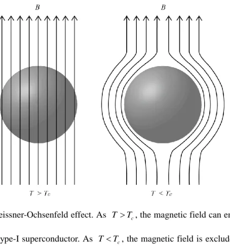
Superconductivity was discovered by Heike Kamerlingh Onnes in 1911 [1]. When the temperature is lower than the critical temperature, where the phase transition takes place, some materials exhibit superconducting behavior. In the superconducting state, resistivity becomes zero and the material excludes the applied external magnetic field from the interior which is called the Meissner-Ochsenfeld effect [2] as shown in figure 2.1.
Figure 2.1 Meissner-Ochsenfeld effect. As T Tc, the magnetic field can enter into the interior of a type-I superconductor. As T Tc, the magnetic field is excluded from the interior.
2.1 Two-fluid Model
Gorter and Casimir proposed a two-fluid model to explain the thermodynamic properties of superconducting phase transition [3]. The two-fluid model proposes that (i) there are two types of free electron, one is normal electron, the other one is superconducting electron which depends on temperature. (ii) a normal electron can scatter with lattice so contribute to entropy and result in resistance (iii) a superconducting electron is in a condensed state which means superconducting electrons condense in lower energy state. When the phase transition occurs, the free energy of superconducting stat is lower than the free energy of normal state
(
2 0
2
c
n s
F F H
), where V is volume of superconductor. (iv) superconducting phase transition belong to second order transition and superconducting state is order state.
2.2 London Equations
In 1935, the following two equations were derived by London and London [4].
2 s
s
B m j
n e , (2.2.1)
2 s s
j n e E
t m
, (2.2.2)
where j is the superconducting current density, e is the charge of an electron, s ns is the number density of superconducting electrons, m is electron mass, B and E are the magnetic and electric field within the superconductor respectively.
Eq. (2.2.1) and Eq. (2.2.2) are called the first and the second London (LD) equations, respectively. Combining Ampere’s law B 0J with the LD equation,
we have
2
2
B 1 B
. (2.2.3)
The solution of Eq. (2.2.3) is
0 xBz x B e. (2.2.4)
This implies that the external magnetic fields are exponentially screened with a characteristic length λ which is called the penetration depth. The penetration depth is
0 s
m
n e
. (2.2.5)
Using Ampere’s law B 0J again with Eq. (2.4), we have
0 x a y
j B e
. (2.2.6)
This implies that current can just flow on the surface with depth .
Although the LD equations are consistent with most experimental results, they cannot explain the mechanism of superconducting behavior. After that, with advances in theory, there are some widely acceptable theories which will be further discussed.
2.3 BCS Theory
In 1957, conventional superconductors were modeled successfully by the pioneering theory developed by John Bardeen, Leon Cooper and Robert Schrieffer in what is called the BCS theory [5]. The BCS theory is different from LD equations, phenomenology equation, and is the first microscopic theory of superconductivity [6].
They suggested that in the superconducting state the electron pairs by lattice vibration (phonon) and form the Cooper pair in which two electrons are bound to each other.
Such a revolutionized concept has won Bardeen, Cooper and Schrieffer the Nobel prize in Physics in 1972.
2.3.1 Cooper Pair
The Cooper pair was proposed by Cooper in 1956 [7]. The basic concept is that in addition to Coulomb repulsion there is some attraction between electrons to form a Cooper pair because the free energy reduces when normal state transfer to superconducting state. The mechanism can be simply explained by a classical method [8]. As shown in figure 2.1, an electron attracts the positive ions and increases the positive charge density nearby. Although there is Coulomb repulsion, this local positive charge area attracts another electron and then pair them up. It can also be explained by the quantum mechanical effect which shows that the attraction is due to electron-phonon interaction. The phonon is a collective vibrational motion of the positively charged lattice [9].
Figure 2.2 Cooper pair diagram.
Although electrons are fermion which cannot occupy the same quantum state due to the Pauli exclusion principle, Cooper pairs, which are composed of two electrons with opposite spin and momentum, are bosons and can occupy the same quantum state because the electron-phonon interaction is long range and the distance is usually greater than distance of electron [10].
2.3.2 Energy Gap
As indicated in previous section superconducting phase transition belongs to second order transition. The physical quantity which correlate with second order transition is specific heat. From the experiment result in Ref.[11], the superconducting specific heat depends on temperature with exponential relation.
1.5 /
9.17 T Tc
es c
c e
T
. (2.3.1)
In statistical mechanics, if there is an energy gap in a single electron system, with increasing temperature the electron must absorb the energy which is equal to energy gap in exciting process and the number of electron is proportional to e/kBT. Therefore, it is expected that there is an energy gap in superconducting state and the energy gap is 2. The energy gap of BCS theory is given
0 1 10
2 sinh 1
0
N V
N V D
De
N V
, (2.3.2)
where N
0 is density of state on the Fermi surface, D is Debye frequency.2.4 Ginzburg-Landau Theory
After the development of the LD equations, Ginzburg also proposed a phenomenology theory which is called Ginzburg-Landau (GL) theory in 1950 and based on the theory of phase transition [12]. Although the GL theory was just a mathematical model for describing the superconducting behavior, Gor’kov prove that the GL theory is a limitation of BCS theory as T Tc from the view of microscopic theory in 1957 [13].
In 1937, Landau proposed a theory of second order phase transition which based on the three postulates. First, there is an order parameter which will be zero when a phase transition take place. Second, free energy can be expanded with by power law.
Third, the coefficient is the function of temperature.
Following Landau’s postulates, Ginzburg developed the theory so-called Ginzburg-Landau (GL) theory and interpret the physics meaning of as 2 ns where ns is the density of superconducting electron. When T Tc , the free energy can be write as
* 2 2
2 4
*
1
2 2 8
GL
s n GL
h e h
F F A
m i c
, (2.4.1)
where Fs is the free energy of a superconductor, Fn is the free energy of a normal state, e* is the charge of pair of electron and e* 2e, which e is the charge of single electron, m*2m and n*s is the number of pair of electron and * 1
s 2 s
n n , where
ns is the number of single electron in the condensate. The first two terms are from Landau’s postulate. The third term is kinetic energy of superconducting electron. The last term is the energy which is induced by magnetic field.
2.4.1 Magnetic Field Dependence of Temperature
To figure out the parameters GL and GL, the case without field and gradient was discussed. Equation (2.4.1) becomes
2 4
2
GL
s n GL
F F . (2.4.2)
Evidently GL must be a positive value for the lowest free energy at the transition point T Tc because the density of superconducting electron ns 2 0 as
T Tc. If the GL is a negative value, the minimum of free energy would occur with any allowed value of 2. Different from the value of GL, GL can be positive or negative value. As T Tc, GL is a negative value and the minimum of free energy
occurs at 2 GL
GL
. As T Tc, GL is a positive value and the minimum of free
energy occurs at 2 0. Therefore GL
T can be written as
c
GL
GL c
T T
T T T d
dT
. (2.4.3)
Now, substituting 2 2 GL
GL
and
c
GL
GL c
T T
T T T d
dT
into equation
(2.4.2)
22 2 2
0
2 2 2 2
c
GL c GL a
s n
GLc GLc T T
T T d H
F F
dT
, (2.4.4)
where GL
Tc GLc, Ha is apparent magnetic fieldFinally, it is a formula about magnetic field dependence of temperature under the limitation approaching Tc
2
c c 0 1
c
H T H T
T
. (2.4.5)
2.4.2 The GL Equation
However, external magnetic field can actually cause the order parameter variant with space. For generation situation, the more complicated case should be discussed. If the order parameter vary with space which means
r , the extra term in Eq (2.4.1) is* 2
*
1 2
h e
m i c A
. (2.4.6)
To solve this, let ei and the remaining term can be written as
2
* 2 2 22
*
1 2
e A
m c
, (2.4.7)
where B r
A r
, B r
is the interior magnetic field. The first term contributes to extra energy associated with gradient. The second term is the kinetic energy with supercurrents in a gauge-invariant form. In this case, Eq (2.4.1) can be rewritten as2 4 * 2 2
*
0
1 1
2 2 1 2
GL
s n GL a
F F i e A B B H
m
. (2.4.8)
The GL equation can be obtained by integrating Eq (2..4.7) with and A, respectively.
*
2 2*
1 + 0
2 i e A GL GL
m , (2.4.9)
with the boundary condition n
i e A
0.
* *2
* * 2
0
1
2 s
e e
B A j
im m
, (2.4.10)
with the boundary condition
0 a 0
n B H
. The equation (2.4.9) and (2.4.10) are
called first GL equation and second GL equation, respectively. Theoretically, GL equation and Maxwell equation can solve
T r H, ,
and A T r
, in most part of superconductor. However, the general solution is too difficult to deal with so, in general situation, the calculation just be an approximation under different condition.2.4.3 The GL Penetration Depth and Coherence Length
Although the general solution of the GL equation cannot be obtained, the GL equations give the two characteristic length to study superconductor in different types superconductor. Firstly, consider another case of weak magnetic field H0
0
with the sample dimensions much greater than the magnetic penetration depth , the second GL equation becomes
*2 2
* 0 s
j e A
m c
, (2.4.11)
taking the curl of both sides and replacing 02 GL
GL
*2 *2
2
* 0 *
GL s
GL
e e
j B B
m c m c
, (2.4.12)
substituting js 4c
B
into Eq (2.4.12)
* 2
*2 0
4
GL GL
m c B B
e
. (2.4.13)
Comparing with London equation, the GL penetration depth is given
* 2 1/ 2
4 *2
GL GL
m c T
T e T
, (2.4.14)
this result is consistent with London penetration depth if 02 n*s
. Substituting
Eq (2.4.14) into Eq (2.4.4) get the parameter GL and GL
* 2*2 2
2GL c
T e H T
m c , (2.4.15)
*2*44 2
44
GL c
T e H T T
m c
. (2.4.16)
The next case is that assuming varies only in one direction z and without external magnetic field. In the case the first GL equation becomes
2 2
2
* 2 0
2 GL GL
d
m dz
, (2.4.17)
if z is real and introduce a new dimensionless order parameter
0
f z z
. (2.4.18)
The Eq (2.4.17) can be rewritten as
2 2
3
* 2 0
2 GL
d f z
f z f z m dz
. (2.4.19)
From Eq (2.4.19), a length scale for spatial variation of the order parameter is given by
1/ 2 2
2 * GL
T m T
, (2.4.20)
which is called the GL coherence length. This two characteristic length are both depend on temperature.
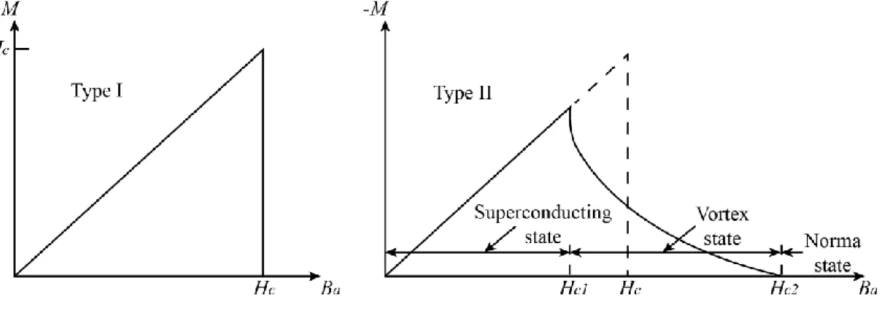
2.5 Type-I and Type-II Superconductor
As pervious mentioned, there are two superconducting characteristics. However, the one of feature is violated in some superconductor. As shown in figure 2.3, there are two different types of superconductor which can be categorized according to their magnetic behaviour.
2.5.1 Magnetization of the Superconductor
A type-I superconductor excludes the whole magnetic field until a critical field Hc.
When the magnetic field exceeds the critical field Hc the superconducting state will be destroyed.
A type-II superconductor can also keep the magnetic field outside until the external magnetic field reach the lower critical field Hc1 and then the magnetic field can enter into the superconductor to form a mixed state. The mixed state means that there are both superconducting state and normal state inside. With increasing magnetic field until upper critical magnetic field Hc2, the superconducting state will be completely broken.
Figure 2.3 Magnetization M versus applied magnetic field H for Type-I and Type-II superconductor.
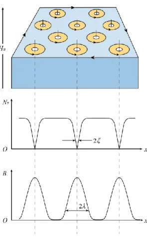
The magnetic field can enter into superconductor in the form of vortex which is surrounded by superconducting current due to Cooper pair motion and the magnetic flux is quantized. The magnetic flux in the vortex is integral multiple of magnetism quantum flux 0.
n0
, (2.5.1)
where n is positive integer and 0 is superconducting magnetic flux quantum with
0 2
h
e.
The radius of vortex is determined by coherence length. As shown in figure 2.4, the magnetic field in the center is equal to external magnetic field and exponentially decay from the core with the decay length which is equal to penetration depth. The lower and upper critical field are also determined by the penetration length and coherence length, respectively.
0
1 2
c 4
H T
T
, (2.5.2)
0
2 2
c 2
H T
T
. (2.5.3)
Figure 2.4 Mixed state of Type-II superconductor
2.5.2 Dimensionless GL Parameter κ
It is known that there are two types of superconductor which can be distinguished by a dimensionless parameter which is so-called GL parameter κ. In the GL theory, there are two characteristic lengths coherence ξ and penetration length λ. By using these two characteristic lengths, define a dimensionless GL parameter κ by
T T
, (2.5.4)
this parameter can be used to distinguish two different types of superconductor by [14].
1 , Type I 2
1 , Type II
, (2.5.5)
2.6 Upper Critical Field Limits
Conventional superconductor is described by BCS which is rely on Cooper pairs.
Because Cooper pairs consist of two electrons with opposite spin and momentum, there are two limitations of upper critical magnetic field which are contributed to two different ways which can possible break Cooper pairs in the presence of an external magnetic field. The first one is orbital limit due to the Lorentz force. The second one is spin paramagnetic limit result from Zeeman effect.
In [15], Werthamer, Helfand and Honenberg (WHH) studied the temperature and purity dependence of the critical field. The temperature dependence of magnetic field and spin-orbit scattering can be expressed
1 1
1 1 1 2 1 1 2 1
ln 2 4 2 2 2 4 2 2 2
SO SO
SO SO
i i
i i
t t t
, (2.6.1)
where
c
t T
T ,
2 1/ 2
2 1
Maki 2 SO
, 0 2
2 2
1
4 c
c t
H dH
dt
,
22 0
0
orb c
Maki P
H
H
and is digamma function. Eq (2.6.5) consider both the orbit limit and the spin limit.
Maki is so-called Maki parameter which can be used to determine which effect dominate the upper critical magnetic field limit, orbit limit or spin limit. SO is a parameter describing the strength of spin-orbit scattering. With WHH theory, Eq (2.6.5) can be used to analyze the experimental result by adjusting the parameter SO and
Maki.
2.6.1 Orbital Limit
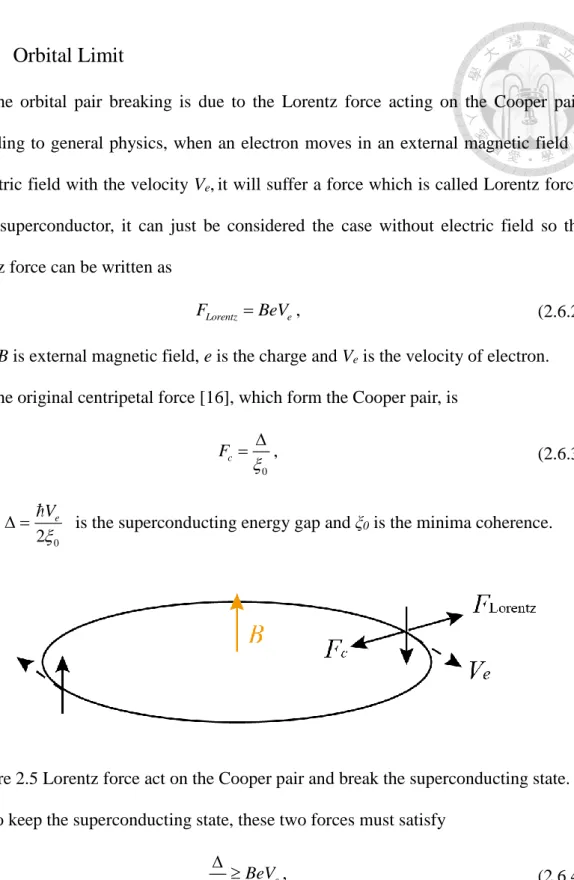
The orbital pair breaking is due to the Lorentz force acting on the Cooper pair.
According to general physics, when an electron moves in an external magnetic field B or electric field with the velocity Ve,it will suffer a force which is called Lorentz force.
In the superconductor, it can just be considered the case without electric field so the Lorentz force can be written as
Lorentz e
F BeV , (2.6.2)
where B is external magnetic field, e is the charge and Ve is the velocity of electron.
The original centripetal force [16], which form the Cooper pair, is
0
Fc
, (2.6.3)
where 2 0
Ve
is the superconducting energy gap and ξ0 is the minima coherence.
Figure 2.5 Lorentz force act on the Cooper pair and break the superconducting state.
To keep the superconducting state, these two forces must satisfy
0
BeVe
, (2.6.4)
under the limit condition,
0
2 2
2 0
Bc
. (2.6.5)
In WHH theory with the absence of spin effect
Maki 0
, the upper critical is restricted by orbit limit. The Eq (2.6.1) can be rewritten as simple one1 1 1
lnt 22t 2
, (2.6.6)
and then the upper critical magnetic field of orbit limit can be derived as
0 20 2 0 0.69
c
orb c
c c
T T
d H
H T
dT
, (2.6.7)
where 0 is vacuum permeability and Tc is the critical temperature.
2.6.2 Spin Paramagnetic Limit
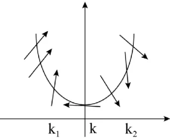
The spin paramagnetic limit results from the Zeeman effect which align the spin of two electrons of Cooper pair with direction of external magnetic field [17, 18]. Zeeman effect is that, with an external magnetic field, the electron orbital momentum and the spin momentum will couple and induce energy splitting. When the spin polarization energy exceeds the superconducting condensation energy, the superconducting behavior will be suppressed. According to the BCS theory, the energy gap at T0 is
0 1.76k TB c [5]. The polarization energy is 1 2
2nHP where 2 2
04
B n
g N
is
the magnetic susceptibility and B is Bohr magneton and N
0 is the density of state on the Fermi surface.Figure 2.6 The spin paramagnetic limit due to the Zeeman effect.
The spin limit can be calculated by the equilibrium of these two energy
21 2
2nHP N 0 2 . (2.6.8)
Substituting 1.76k TB , 2 2
04
B n
g N
and g2 (for free electron) into Eq
(2.6.8), the Pauli paramagnetic limit can be expressed by
P 1.85 c
H T . (2.6.9)
The spin paramagnetic can be possibly enhanced in the case of strong electron-phonon coupling, spin-orbital coupling or pairing state [19].
2.7 Spin-orbit Interaction
2.7.1 Spin-orbit interaction
The electrons can be thought of a spinning charge ball and the correlated angular momentum is spin. The interaction of the electron spin with the electric field which is related magnetic field in the electrons rest frame with the lattice motion is so-called spin-orbit interaction.
2.7.2 Elliot-Yafet mechanism
There are different mechanisms to explain spin-orbit interaction. The Elliot-Yafet (EY) mechanism is generally used to explain spin-orbit interaction in Al. Elliott propose that spin-orbit interaction will cause different wave function from all band mixed so electron momentum change in the process of momentum relaxation which means that the spin-orbit scattering can flip the spin of electron. If the EY mechanism lead the scattering mechanism, the momentum scattering time is proportional to the spin relaxation time [20].
Figure 2.7 Spin polarizations at different wavevector.
The spin-orbit interaction can play a role in superconductivity. Previously our group have already studied this effect and show that with the decreasing thickness the spin-orbit interaction can be strong which is indicated by the decreasing spin-orbit relaxation time and it also consistent with the results of this thesis [21].
2.8 BKT Transition
The Berezinskii-Kosterlitz-Thouless (BKT) transition is a topological transition in 2D system. This topological transition is related to topological charge excitation process.
In superconducting state, vortex and anti-vortex can be seemed as topological charged.
In a 2D superconducting system vortex-antivortex pairs which is bound at low temperatures would dissociate into free vortices at a characteristic transition Temperature TBKT. Because the ordered state has power law decay and the disordered state has exponential decay, by electronic properties measurement, an easy way to find the BKT transition is to observe the relation between voltage and current. The BKT transition occurs where V~I3 [22-25]. Our group member have already showed the BKT transition in Al with different methods and the results are consistent with each other [26].
REFERENCES
[1] H. K. Onnes, Leiden Comm. (1911).
[2] W. Meissner and R. Ochsenfeld, Naturwiss, 21, 787 (1933).
[3] C. J. Gorter and H. B. G. Casimir, Phys, 1, 306 (1934a) [4] F. London and H. London, Proc. R. Soc., A, 155, 71 (1935).
[5] J. Bardeen, L. N. Cooper and J. R. Schrieffer, Phys. Rev. 108, 5 (1957).
[6] J. Bardeen, L. N. Cooper and J. R. Schrieffer, Phys. Rev. 106, 162 (1957).
[7] Leon Cooper, Phys. Rev. 104, 1189 (1956).
[8] Alan M. J. Kadin, Supercond. Nov. Mag. 20(4), 285 (2005)
[9] Shigeji Fujita; Kei Ito; and Slavador Godoy, (2009). Quantum Theory of Conducting Matter. Springer Publishing. pp. 15–27.
[10] Richard P. Feynman, Robert Leighton; and Matthew Sands. Lectures on Physics, Vol.3. Addison–Wesley. pp. 21–7, 8. (1965)
[11] W. S. Corak, B. B. Goodman, C. B. Satterthwaite, and A. Wexler, Phys. Rev. 102, 656 (1956).
[12] V. L. Ginzburg and L. D. Landau, J. Exp. Theor. Phys. (USSR) 20, 1064 (1950).
[13] L. P. Gor’kov Sov. Phys. JETP 36, 6 (1959)
[14] A. A. Abrikosov, J. Exp. Theor. Phys. (USSR) 32, 1442 (1957).
[15] N. R. Werthamer, E. Helfand and P. C. Honenberg, Phys. Rev. 147, 295 (1966)) [16] http://web.mit.edu/6.763/www/FT03/Lectures/Lecture17.pdf
[17] A. M. Clogston, Phys. Rev. Lett. 9, 6 (1962).
[18] B. S. Chandrasekhat, Appl. Phys. Lett. 1, 1 (1962).
[19] J. L. Zhang, L. Jiao, Y. Chen, H. Q. Yuan, Phys. Condens. Matter. 6, 463 (2012).
[20] R. J. Elliott Phys. Re. 96 266 (1954).
[21] S.-T. Lo, S.-W. Lin, Y.-T. Wang, S.-D. Lin and C.-T. Liang, Sci. Rep. 4, 5438 (2014).
[22] A. F. Hebard and A. T. Fiory, Phys. Rev. Lett. 44, 291 (1980).
[23] N. D. Mermin and H. Wanger, Phys. Rev. Lett. 17, 1307 (1966).
[24] M. R. Beasley, J. E. Mooij and T. P. Orlando, Phys. Rev. Lett. 42, 1165 (1979).
[25] D. S. Fisher, M. P. Fisher, and D. A. Huse, Phys. Rev. B 43, 1130 (1991).
[26] Guan-Ming Su, “Studies of Kosterlitz–Thouless Transition: Numeric Simulation of the 2D XY Model and 2D Superconductivity in 4-nm Aluminum Nano-Film,”
M.S. thesis, National Taiwan University, Taiwan, 2018.
Chapter 3 Device fabrication and Measurement Technique
This chapter will cover the device fabrication and measurement technique. The aluminum (Al) films were prepared by Prof. Sheng-Di Lin’s group at NCTU using molecular beam epitaxy (MBE) system. The measurement was performed by Prof.
Chi-Te Liang’s group at NTU using a cryo-free He3/He4 dilution refrigerator.
3.1 Device Fabrication
In this section, I will briefly introduce the concept of MBE and the fabrication process of the device. The detailed growth processes can be found in Ref. [1].
3.1.1 Molecular-beam Epitaxy
The MBE technique was developed by Arthur and Cho in 1960s at Bell Laboratories [2]. It is usually used to grow nanostructure device with controllable thickness and high quality. Under the condition of ultra-high vacuum, by heating up the material to sublime, the gaseous elements will condense on substrate. The atoms condense on surface of substrate slowly and systematically in ultra-thin layer. The quality was mainly influenced by deposition rate which is tuned by temperature and pressure.
3.1.2 Fabrication Processes
The fabrication processes can be divided into three parts. First, the substrate was baked for cleaning the surface. The second part is growing Al by MBE. Finally, the device was shaped into a Hall-bar for electrical property measurement.
(i) Baking substrate:
As shown in figure 3.1, there are three stages of this process for removing the steam, organic and oxidized layer respectively. The substrate was baked for 8 hours at 200 C and then backed for 5 hours at 400 C, and finally baked for 20 minutes at 600
C.
Figure 3.1 Baking substrate process.
(ii) Growing Al:
Under the condition of Ga-rich, the Al nanofilm can be grown with high quality and flat surface. For this purpose, the substrate was grown a 200-nm-thick undoped GaAs buffer layer at 580 C and then heated up to 600 C without arsenic flux to transform the surface into Ga-rich condition for 3 minutes. After that, the sample was cooled down and subsequently Al was grown on the surface at the rate of 0.1 nm/s.
(iii) Hall-bar fabrication
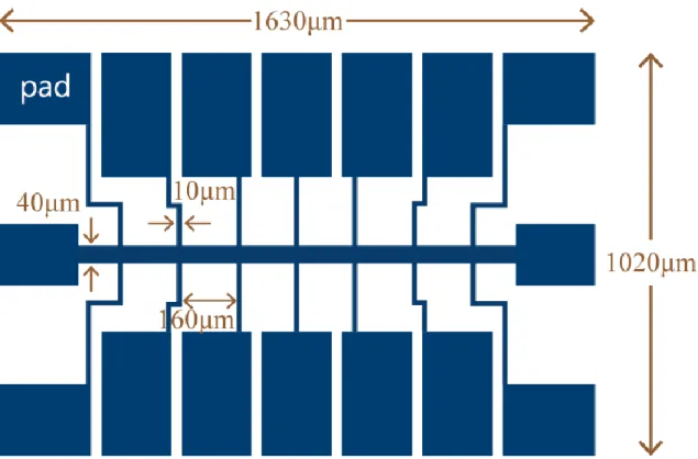
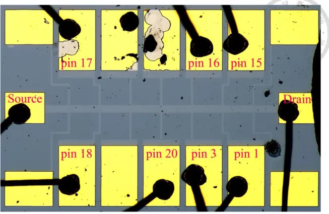
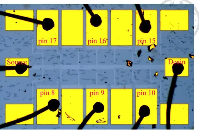
For electrical measurements, Al nanofilms were shaped into Hall-bar by photolithography. The fabrication started with exposure, followed by development which was using TMAH developer to shape the Hall-bar. Next, the exposure and the development which was using AZ developer was applied again to form the pad and then using E-gun deposited 200 nm thick Al layer to protect Al etched by followed procedure and then grown Al2O3 with atomic layer deposition (ALD) to form passivation. The last step was using BOE etching on the region of pad and depositing Ti and Au of 20 nm and 200 nm respectively for contact.
The size of device was shown in figure 3.2 with the length of device is 1630 μm × 1020 μm and the width of Hall-bar are 100 μm and 40 μm. The OM image is shown in figure 3.3-3.5 for 3-nm-thick, 3.5-nm-thick and 4-nm-thick, respectively.
Figure 3.2 schematic diagram of device.
Figure 3.3 OM image of 3-nm-thick device.
Figure 3.4 OM image of 3.5-nm-thick device.
Figure 3.5 OM image of 4-nm-thick device.
3.2 Low-temperature System
The experiments were performed in an Oxford Triton 200 cryo-free He3/He4 dilution refrigerator. The dilution refrigerator is a cryogenic system which can cold down to around 20 mK. The concept was proposed by Heinz London in early 1950s and realized in 1964 [3]. The mechanism relies on thermodynamic characteristics of the mixture of two isotopes of He3 and He4. As shown in figure 3.6, when cooled below a critical temperature (about 870 mK) the mixture is spontaneously separated into two liquid phase which is divided by a phase boundary. The working fluid is He3 which is circulated by vacuum pumps. When the He3 moves from the He3-rich phase (right of triple point) to the He4-rich phase (left of the triple point), it expand and take heat out of the chamber and then reduce the temperature.
Figure 3.6 The phase diagram of He3 and He4 mixture.(Take from [4])
3.3 Four-terminal DC Measurements
Standard four-terminal dc resistance measurements were performed on the devices.
As shown in figure 3.7, the device’s source was connected to a Keithley 2400 multi-meter which providing a current from source to drain. The voltage drops between each voltage probes was measured by Keithley 2000 multi-meter.
The advantage of using four-terminal measurement is that the influence of contact resistance can be diminished.
Figure 3.7 The schematic of four-terminal measurement of 3.5-nm-thick device.
REFERENCES
[1] Y.-T. Fan, M.-C. Lo, C.-C. Wu, P.-Y. Chen, J.-S. Wu, C.-T. Liang, and S.-D. Lin, AIP Adv. 7, 075213 (2017).
[2] A. Y. Cho and J. R. Arthur Prog. Solid State Chem. 10, 157 (1975).
[3] P. Das R. Bruyn de Ouboter, and K. W. Taconis. A Realization of a London-Clarke-Mendoza Type Refrigerator.
[4] http://ltl.tkk.fi/research/theory/mixture.html
Chapter 4 Results and Discussion
Four-terminal dc measurement was performed on our devices which are of different thickness (3-nm-thick, 3.5-nm-thick and 4-nm-thick) to measure the current-voltage (I-V) curves. The process and correlated machine is mentioned in Chapter 3.
4.1 Electronic Properties of MBE-Grown Al Nanofilms
-4 -2 0 2 4
-0.02 0.00 0.02
2.4 K
V (V)
I ()
2.0 K
Figure 4.1 I-V curves of the 3-nm-thick Al nanofilm at various temperatures.
-20 -10 0 10 20 -0.04
-0.02 0.00 0.02 0.04
2.5 K
V (V)
I (A)
2.35 K
Figure 4.2 I-V curves of the 3.5-nm-thick Al nanofilm at various temperatures.
-1.0 -0.5 0.0 0.5 1.0
-0.06 -0.04 -0.02 0.00 0.02 0.04 0.06
2.30 K
V (V)
I (mA)
0.25 K
Figure 4.3 I-V curves of the 4-nm-thick Al nanofilm at various temperatures.
Figures 4.1-4.3 show I-V characteristics of the 3-nm, 3.5-nm and 4-nm-thick Al nanofilms at different temperatures, respectively. When the temperature is lower than the critical temperature and the current is lower than the critical current, our samples show the zero-resistance state which is a superconducting behavior. The transition is sharp which indicate good quality of Al nanofilm and I define the critical current at the certain point which it shows an abrupt change to the normal state at the lowest temperature (0.25 K). At lowest temperature 0.25 K, the critical currents are 13.6 μA, 64.55 μA, and 820 μA for the 3-nm-thick, 3.5-nm-thick, and 4-nm-thick samples, respectively.
1E-7 1E-6
1E-4 1E-3 0.01
2.4 K
2.0 K
V (V)
I (A)
slope=3
Figure 4.4 I-V curves of the 3-nm-thick device for various temperatures on a log-log scale. The black straight line corresponds to V~I3.
10-6 10-5 1E-4
1E-3 0.01 0.1
2.5 K
V (V)
I (A)
slpoe=3
2.35 K
Figure 4.5 I-V curves of the 3.5-nm-thick device for various temperatures on a log-log scale. The black straight line corresponds to V~I3.
10-4 1E-4
1E-3
0.01 2.3 K
V (V)
I (A)
slope=3
1.9 K
Figure 4.6 I-V curves of the 4-nm-thick device for various temperatures on a log-log
The data shown in figures 4.4-4.6 are extracted from figures 4.1-4.3. In these figures, the I-V curves was plotted at different temperatures on a log-log scale. The red line with slope 3 was drawn to find when the BKT transition take place. The linear fit was applied to find the slope α
V ~I
at each temperature and the temperature dependence of the exponent α is plotted in figures 4.7-4.9. The BKT transition temperature will be determined when find where the slope of the fit is 3.1.9 2.0 2.1 2.2 2.3 2.4 2.5 2.6
0 2 4 6 8 10 12
T (K)
TBKT=2.25 K
Figure 4.7 α(T) obtained on the 3-nm-thick device. The data are extracted from those shown in figure 4.4.
2.34 2.36 2.38 2.40 2.42 2.44 2.46 2.48 2.50 2.52 1
2 3 4 5 6 7 8
T (K) TBKT=2.4 K
Figure 4.8 α(T) obtained on the 3.5-nm-thick device. The data are extracted from those shown in figure 4.5.
1.8 2.0 2.2 2.4
0 2 4 6 8 10 12 14
T (K)
TBKT=2.1 K
Figure 4.9 α(T) obtained on the 4-nm-thick device. The data are extracted from those shown in figure 4.6.
In figures 4.7-4.9, the slope at temperature was found. At where the slope is 3 indicate the BKT transition occurring. At higher temperatures, the slope is 1 which indicates the metallic behavior. The BKT transition temperature (TBKT) of the 3-nm, 3.5-nm and 4-nm thick films are 2.25 K, 2.4 K and 2.1 K, respectively.
0 2 4 6 8 10
0 1000 2000 3000 4000 5000 6000 7000
R ()
T (K) Tc= 2.33 K
Figure 4.10 R-T curve of the 3-nm-thick device.
0 2 4 6 8 10
0 500 1000 1500 2000 2500
R ()
T (K) Tc= 2.44 K
Figure 4.11 R-T curve of the 3.5-nm-thick device.

![Figure 3.6 The phase diagram of He 3 and He 4 mixture.(Take from [4])](https://thumb-ap.123doks.com/thumbv2/9libinfo/9603713.630029/40.892.163.781.118.531/figure-phase-diagram-mixture.webp)
