Schottky barrier heights of metal contacts to n-type gallium nitride
with low-temperature-grown cap layer
M. L. Lee
Department of Electro-Optical Engineering, Southern Taiwan University of Technology, No.1, Nantai St, Yung-Kang City, Tainan 710, Taiwan
J. K. Sheua兲and S. W. Lin
Institute of Electro-Optical Science and Engineering, National Cheng Kung University, Tainan 70101, Taiwan
共Received 16 August 2005; accepted 16 December 2005; published online 18 January 2006兲 The Schottky barrier heights of metal contacts, including WSi0.8, Cr, Ti, Pt, and Ni, on n-type gallium nitride共GaN兲 with a GaN cap layer grown at low-temperature 共LTG兲 were studied. Higher barriers can be formed by introducing LTG GaN on top of the conventional structures. The higher Schottky barrier observed in samples with the LTG GaN cap layer may be due to the facts that the high-resistivity LTG GaN layer may passivate the surface defects 共pits兲 formed from threading dislocations or it may cause the Fermi-level pinning effect at the metal/semiconductor interface, revealing a weak dependence of Schottky barrier height on the metal work function. The measured barrier heights of the LTG GaN-capped samples were 1.02– 1.13 eV. © 2006 American Institute of
Physics. 关DOI:10.1063/1.2166477兴
Gallium nitride 共GaN兲 and its related alloys have great potential for use in field-effect transistors共FETs兲 operated at high-power, high-temperature, and high-frequency, because the band gap is wide. However, the large gate leakage cur-rent, which is obtained at high temperature or high bias, limits the performance of the device. The leakage current in the Schottky contacts共SCs兲 depends strongly on the barrier height. The fact that various metals1–4 and transparent con-ducting oxide films5have been deposited on GaN to produce high-performance SCs is well known. The leakage current of SCs also depends strongly on the threading dislocation共TD兲 density of the GaN.6 It is also well known that the barrier height and/or reverse leakage current of Schottky barrier di-odes 共SBDs兲 also depend strongly on the properties of the surface layer. Studies have demonstrated that the gate leak-age current in FETs can be reduced markedly using a low-temperature-grown 共LTG兲 cap layer.7 In this study, a LTG GaN layer was deposited on top of an undoped GaN layer to yield a surface state that differed from that on conventional high-temperature-grown 共HTG兲 GaN films, and GaN SBDs were fabricated using different metals as Schottky contacts.
The wafers used herein were all grown on the c-face 共0001兲 sapphire 共Al2O3兲 substrates by organometallic vapor phase epitaxy. After the sapphire substrate was annealed at 1100 ° C in H2 ambient to remove surface contamination, a 30 nm thick GaN nucleation layer was deposited onto the sapphire substrate at 550 ° C. The temperature was then increased to 1060 ° C to grow a 3m thick Si-doped
n+-GaN 共n=3⫻1018cm−3兲 layer. On top of this n+-GaN layer, a 1m thick undoped GaN 共i-GaN兲 followed by a 30 nm thick LTG GaN was grown as a cap layer共Sample A兲. The growth temperature of the LTG GaN cap layer was 550 ° C. Notably, this LTG GaN cap layer behaves like an insulator with a sheet resistivity of greater than 109⍀/cm. Samples without the LTG GaN cap layer were also prepared
for comparison共Sample B兲. In this work, GaN SBDs were fabricated by dry etching to expose the n+-GaN; this was followed by the deposition of Ti/ Al 共20/100 nm兲 on the exposed n+-GaN as an Ohmic contact. Finally, various met-als, including WSi0.8, Ti, Cr, Pt, and Ni were deposited on the LTG GaN layer to serve as Schottky metals. The WSi0.8 films were deposited on GaN samples using a W / Si co-sputtering process with an Ar discharge. The diameter of the fabricated circular devices was maintained at 500m. The room-temperature 共RT兲 current-voltage 共I-V兲 characteristics of the fabricated SBDs were then measured using an HP4156 semiconductor parameter analyzer.
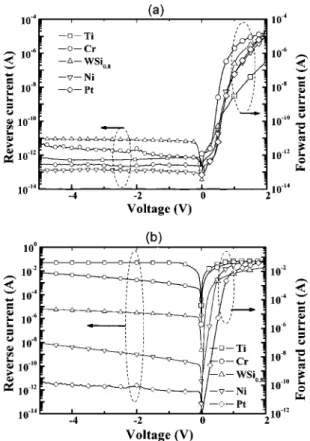
Figure 1共a兲 shows the typical I-V characteristics of the
n-GaN/metal SBDs taken at RT. In the example of n-GaN / Ni/ Au SBDs, the reverse-bias current is around
1⫻10−11– 1⫻10−13A for samples of A. Samples of B with Ni/ Au contacts exhibited a high reverse current of 1⫻10−10– 1⫻10−8A, as shown in Fig. 1共b兲. The low re-verse current is attributable to the highly resistive LTG GaN cap layer between Ni and the undoped GaN layer, which may have increased potential barrier above that of conventional SBDs共Sample B兲. The lower forward current observed from Sample A is attributable to the high-resistivity LTG GaN cap layer and the fact that the poor crystal quality associated with the trap levels within the bandgap of LTG GaN,8 compen-sates for the injected carriers, as in annealed LTG GaAs, which thus has high resistivity.9 In contrast, the preliminary results herein revealed that no significant change in resistiv-ity is observed between the as-grown LTG GaN and the an-nealed LTG GaN films. Similar I-V characteristics of various metals on the LTG GaN surface were also observed. As shown in Fig. 1, the typical I-V characteristics of various SBDs, including GaN / Ti/ Au, GaN / Pt/ Au, GaN / Cr/ Au, and GaN / WSi0.8/ Au, exhibit similar trends, as observed in GaN / Ni/ Au SBDs.
For an ideal Schottky diode, thermionic emission domi-nated current transport. However, some other effects, includ-ing the field-dependence tunnelinclud-ing through the barrier height
a兲Author to whom correspondence should be addressed; electronic mail:
APPLIED PHYSICS LETTERS 88, 032103共2006兲
0003-6951/2006/88共3兲/032103/3/$23.00 88, 032103-1 © 2006 American Institute of Physics
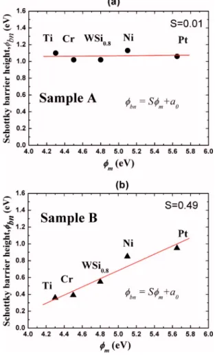
and the generation in the depletion region, may pertain. These effects all result in a deviation from ideal thermionic emission. In this work, the carrier transport is assumed to be governed by the thermionic emission theory. Therefore, the effective barrier heights of Samples A and B can be tenta-tively determined from the forward I-V characteristics. Table I shows the average values of the effective barrier heights of Samples A and B. Notably, the values in Table I were ob-tained for at least 15 samples of A and 15 samples of B. The effective Schottky barrier heights of samples of B with Ni/ Au contacts were estimated to be around 0.85 eV, which is lower than the theoretical value共Schottky–Mott theory兲 of around 1.05 eV, if the work function of Ni and the electron affinity of n-type GaN are 5.15 and 4.1 eV, respectively.10,11 The barrier height of the contact with n-type GaN without the cap layer共Sample B兲 may be lower because of the sur-face defects in the GaN films, including sursur-face pits that originated in the terminations of the TDs. Hierro et al.12 suggested that the presence of charged states in the vicinity
of dislocations is responsible for the locally high reverse leakage current in GaN SBDs and a related decrease in the Schottky barrier height. Therefore, the barrier height ob-served from samples of B may be lower because of the posi-tively charged surface states caused by GaN surface pits originated from the terminations of the TDs. However, the effective barrier height of samples of A with Ni/ Au contacts was as high as 1.13 eV. This value was higher than those of samples of B because the surface states共pits兲 may be passi-vated 共covered兲 by the LTG GaN cap layer to lead to a re-duction of the leakage current and thereby increase the bar-rier height.6 However, this value slightly exceeds the theoretical value of around 1.05 eV, which is the difference between the work function of Ni and the electron affinity of
n-type GaN. Therefore, as well as the above, other
possibili-ties, such as Fermi-level pinning at the metal/low-temperature GaN interface, cannot be ruled out. The Schottky barrier heights of various metals to n-type wurtzite GaN have been systematically studied and the experimental data reveal that the barrier heights varied approximately with the work function of the metal.13According to Table I, the Schottky barrier heights of metal films deposited on n-type GaN with and without LTG GaN cap layer followed a similar trend to the aforesaid n-GaN / Ni/ Au Schottky barrier diodes. For samples of B, the measured barrier height is consistent with the reported values.1,14It is well known that the reason-able growth temperature of high-quality GaN is around 1000 ° C. The LTG GaN cap layers were grown at 550 ° C. Therefore, their crystalline quality is far inferior to that of HTG GaN. As stated above, the LTG GaN layers are highly resistive, and so behave like an insulator. When the surface of HTG GaN was capped with an LTG GaN layer, TD-related surface pits, which form a leakage path on HTG GaN, can be passivated. However, the surface of the poor-quality LTG GaN layers had very high-density surface states. There-fore, Fermi-level pining caused by the high-density surface states may lead the measured barrier height to be around the difference between the energy band gap, Eg, and the neutral level, 0, which is bn⬇Eg/ e-0. The Schottky barrier height seems to be fixed at around 1.0 eV, which corre-sponds to a 0 of around 2.4 eV above the valence band, independently of the difference between the metals 共work functions兲. Figure 2共a兲 shows schematic band diagrams near the metal/LT GaN interface when the Fermi level is pinned at the LTG GaN surface. As speculated above, the thicker bar-rier combined with the Fermi-level pining will lead to a re-duction of the reverse-biased leakage current in samples of A, as shown in Fig. 1, and thereby increase the barrier heights. However, as shown in Fig. 2共b兲, the lower and thin-ner barrier may be responsible for the higher reverse-biased leakage current in samples of B which may be caused by other leakage paths, such as the surface pits that originate from the termination of TDs.6 Defects at the metal/ semiconductor interface affect the I-V characteristics of Schottky diodes because defects may act as recombination centers or as intermediate states in the trap-assisted tunneling of current 关process 3 in Fig. 2共b兲兴. These traps may also combine metal/n-GaN interface states with deep-level bulk states within the tunneling distance of the interface. The deep-level interface states are at least combinations of states associated with the TDs that reach the GaN surface. Either of these mechanisms increases the leakage current and lowers the barrier.
FIG. 1. Typical I-V characteristics of the GaN / Ti/ Au, GaN / Ni/ Au GaN / Pt/ Au, GaN / Cr/ Au, and GaN / WSi0.8/ Au, SBDs taken at room
tem-perature共a兲 with 共b兲 without low-temperature GaN cap layer.
TABLE I. Typical Schottky barrier heights, determined from I – V charac-teristics. The data are averages over at least 15 diodes; the standard devia-tion of the barrier height is 0.01.
Metal 关work function 共eV兲兴 Sample A bn共eV兲 Sample B bn共eV兲 Ti共4.3兲 1.10 0.36 Cr共4.5兲 1.02 0.39 WSi0.8共⬃4.8兲 1.02 0.55 Ni共5.15兲 1.13 0.85 Pt共5.65兲 1.06 0.95
032103-2 Lee, Sheu, and Lin Appl. Phys. Lett. 88, 032103共2006兲
For further clarity, various metals were deposited on
n-type GaN with a LTG GaN cap layer to measure the
effec-tive Schottky barrier heights. As shown in Fig. 3共a兲 and Table I, the measured barrier heights depend very weakly on the metal work functions. The measured Schottky barrier heights ranged from 1.02 to 1.13 eV when different metals
were used. In contrast, in Fig. 3共b兲 and Table I, the measured barrier heights of various metals on n-type GaN without an LTG GaN cap layer 共samples of B兲 depended markedly on the work functions of the metals, and the measured Schottky barrier heights varied from 0.36– 0.95 eV. This preliminary finding supports the tentative proposition that the pinning of the Fermi level at the surface is responsible for the higher SBH, almost fixed at 1.0 eV, of the metal contacts on n-type GaN with an LTG GaN cap layer. In a practical metal/ semiconductor system, the Schottky barrier height can be empirically expressed as bn= Sm+ a0, where S is a slope parameter and a0is a constant. For samples of A, the param-eters of S and a0 determined from the measured Schottky barrier height values are 0.01 and 1.06, respectively, corresponding to a high surface state density of 1014– 1015cm−2eV−1.15
In summary, different metals were deposited on n-type GaN with a LTG GaN cap layer to study SCs. The Schottky barrier was higher in the samples with the LTG GaN cap layer because the high-resistivity LTG GaN may passivate the surface defects共pits兲 caused by dislocations, and it may cause Fermi-level pinning at the metal/semiconductor inter-face. In the latter case, the measured Schottky barrier heights of metals on the LT GaN depended weakly on the work function of the metals. The typical barrier height was around 1.0 eV, even when the work functions of the metals ranged from 4.3 eV共Ti兲 to 5.65 eV 共Pt兲.
The authors would like to thank the Center for Micro/ Nano Technology Research, National Cheng Kung Univer-sity, Tainan, Taiwan, for equipment access and technical sup-port, and the National Science Council of Taiwan for financially supporting this research under Contract No. NSC94-2215-E-006-015. The authors also thank Professors W. C. Lai, Y. K. Su and S. J. Chang for their useful discussion.
1X. A. Cao, S. J. Pearton, G. Dang, A. P. Zhang, F. Ren, and J. M. Van
Hove, Appl. Phys. Lett. 75, 4130共1999兲.
2Q. Z. Liu, L. S. Yu, S. S. Lau, J. M. Redwing, N. R. Perkins, and T. F.
Kuech, Appl. Phys. Lett. 70, 1275共1997兲.
3L. Wang, M. I. Nathan, T.-H. Lim, M. A. Khan, and Q. Chen, Appl. Phys.
Lett. 68, 1267共1996兲.
4C. T. Lee, Y. J. Lin, and D. S. Liu, Appl. Phys. Lett. 79, 2573共2001兲. 5J. K. Kim, H. W. Jang, C. M. Jeon, and J.-L. Lee, Appl. Phys. Lett. 81,
4655共2002兲.
6J. K. Sheu, M. L. Lee, and W. C. Lai, Appl. Phys. Lett. 86, 052103
共2005兲, and references therein.
7L. W. Yin, Y. Hwang, J. H. Lee, R. M. Kolabas, R. J. Trew, and U. K.
Mishra, IEEE Electron Device Lett. 11, 561共1990兲.
8M. Lampert and P. Mark, Current Injection in Solids共Academic, New
York, 1970兲.
9A. Osinsky, S. Gangopadhyay, R. Gaska, B. Williams, M. A. Khan, D.
Kuksenkov, and H. Temkin, Appl. Phys. Lett. 71, 2334共1997兲.
10J. Kim, F. Ren, A. G. Baca, and S. J. Pearton, Appl. Phys. Lett. 82, 3263
共2003兲.
11X. A. Cao, S. J. Pearton, F. Ren, and J. R. Lothian, Appl. Phys. Lett. 73,
942共1998兲.
12A. Hierro, D. Kwon, S. A. Ringela, M. Hansen, J. S. Speck, U. K. Mishra,
and S. P. DenBaars, Appl. Phys. Lett. 76, 3064共2000兲.
13A. C. Schmitz, A. T. Pong, M. A. Khan, Q. Chen, J. W. Yang, and I.
Adesida, J. Electron. Mater. 27, 255共1998兲, and references therein.
14Q. Z. Liu, L. S. Yu, F. Deng, S. S. Lau, and J. M. Redwing, J. Appl. Phys. 84, 881共1998兲, and references therein.
15S. M. Sze, Physics of Semiconductor Devices共Wiley, New York, 1983兲, p.
270. FIG. 2. Schematic energy band diagram of metal/n-GaN Schottky barrier
diodes under reverse bias共a兲 with 共b兲 without LT GaN cap layer. The labeled processes共1兲, 共2兲, 共3兲, and 共4兲 described the current transport via thermionic emission, trap-assisted tunneling, thermonic-field emission tunneling, and field emission tunneling, respectively.
FIG. 3. Schottky barrier heights of different metal contacts on n-type GaN 共a兲 with 共b兲 without LTG GaN cap layer as a function of metal work function.
032103-3 Lee, Sheu, and Lin Appl. Phys. Lett. 88, 032103共2006兲