Low-cost nanofabrication of nanorod InGaN/GaN multiple-quantum-wells light-emitting diodes
Min-Huan Wang, Han Li, Yi-Kai Huang, Wei-Chih Lai, Jinn-Kong Sheu* and Yun-Chorng Chang*
Department of Photonics, National Cheng Kung University, Tainan 701, Taiwan
Abstract:
In this study, we will demonstrate an economic method to fabricate InGaN/GaN nanorod light-emitting diodes (LED). The method is based on top-down approach where GaN layers are etched by combination of dry inductive- coupled plasma (ICP) and wet etches. The nanopatterns are either accomplished by low-cost Nanosphere
Lithography or Nanospherical-Lens Lithography. The top contact of this rod-shape and p-side up LED is accomplished by either a thin layer of graphene or metal nanohole membranes. Optical and electrical
characterizations of these LEDs will also be presented. We believe the fabricated nanorod LED will demonstrates new properties that will be useful for current LED industries.
Introduction:
Modern light-emitting diodes (LEDs) have been improved to a record-high efficiency with a unbelievable pace.
However, to further improve the efficiency, newer concepts are very crucial. Nanophotonics provides new and novel ways to manipulate the emitted photonics, which has been proved to be able to improve the device’s
performance. The expensive fabrication cost to fabricate the necessary nanostructures proved to be the bottleneck for the penetration of these nanostructures into current industrial applications of LEDs.
In this study, we will propose a low-cost nanofabrication method to fabricate nanorod LED. The method is based on top-down approach where GaN layers are etched by combination of dry inductive-coupled plasma (ICP) and wet etches. The etch mask will be patterned by low-cost Nanosphere Lithography (NSL) or Nanospherical-Lens
Lithography (NLL) that have been developed in our group for the last few years. The most difficult steps for this research is to fabricate the top contact to the nanorods. We proposed to use either a thin layer of graphene or metal nanohole membranes fabricated by NLL. Optical and electrical characterizations of these LEDs will also be presented. We believe the fabricated nanorod LED will demonstrates new properties that will be trigger new design of LED for the future LED industries.
Experimental procedures:
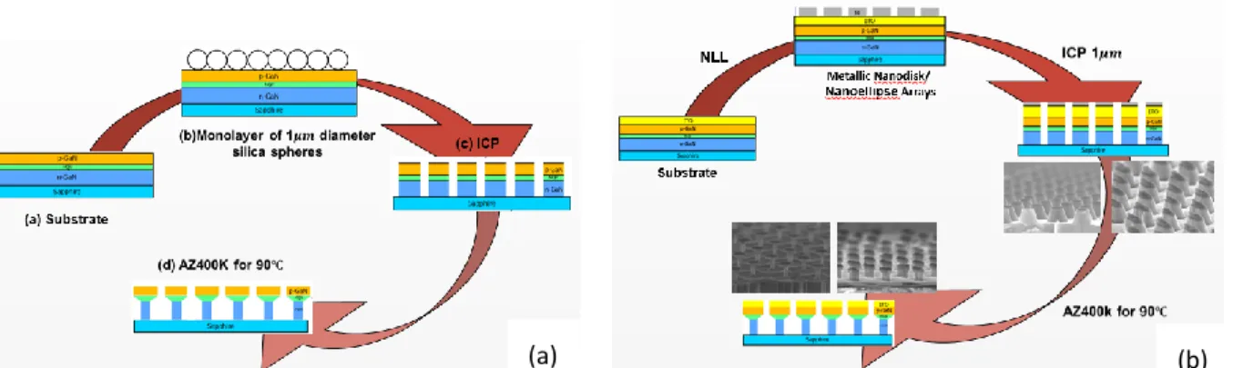
For the two-step etch method using silica nanospheres as the etch mask. First, a close-packed monolayer of 1μm diameter silica spheres is self-assembled on the GaN surface. The silica spheres are as a hard mask for the
following dry ICP etches. The dry ICP etching will create cone-shaped nanorods. Following the dry ICP etch, they used a selective KOH-based wet etch to treat the nanorods. The etchant is AZ400K, which is a kind of photoresist developer. They found out that the wet etch using AZ400K is anisotropic and n-type GaN etches more quickly than p-type GaN. The end result is a “flashlight”-shaped nanorod LEDs. The etch difference is very distinct as you can see the MQW in the SEM images separating n- and p-types GaN. The wet etch method is very interesting as they can not only smooth the surface but also revmove the damages caused by dry ICP etches. However, it is still not easy to fabricate top contacts to these vertically aligned nanorod LEDs. In addition, we also found out that the resulting diameters of the fabricated nanorod is limited by the available sizes of the silica nanospheres. The tuning ability is very limited using this method.
Then, in the second steps, we will start to use the metallic nanodisks or nanoellipses fabricated using NLL as the hard mask for the dry ICP etch. First, the substrate is coated with a thin layer of photoresist and aligned a single-
layer of polystyrene nanospheres on top of it. Following a standard UV exposure and PR developing, PR nanohole arrays can be observed. Nanodisk can be fabricated following metal deposition and lift-off process. If we use a UV lamp as the light source, we can fabricate nano-ellipse arrays using similar processes.
Fig. 1. (a) The detailed procedure of the two-step etch method using silica nanospheres as the etch mask. (b) The detailed procedure of the two-step etch method using the metallic nanodisks or nanoellipses fabricated using NLL as the hard mask for the dry ICP etch.
Results and discussion:
As you can see in the Fig. 2(a), we also obtain the cone-shaped nanorod LED. After dry etch, we also perform wet etch and observe the size variation after different etch durations, as you can see in the Fig. 3. We also observe that n-GaN etches more quickly compare to p-GaN. The measured etch rate for p-GaN is 2.14nm/min. The etch rate for n-GaN is faster at 5.14nm/min. And resulting width of p-GaN is tunable between about 730nm to
400nm.The width of n-GaN is tunable between about 1000nm to 150nm. In this slides, we have demonstrate the ability to reproduce the results shown in the reference paper. But the shape of the LED is not the flashlamp like but a goff-tee like shape.
Fig. 2. After dry ICP etch of 1μm:(a) Cross-section (b) Top-view SEM image
Fig. 3. After wet etch of different etch durations Fig. 4. The measured etch rate for p-GaN and n-GaN During the experiment, we also noticed one interesting results if we used a ITO-coated LED structures as our substrate. Apparently, the wet GaN etch does not etch ITO and the diameter of the top ITO disk does not change with the increasing wet etch duration. The will results in a mushroom-like nanorod as you can clearly observed in the Fig. 5. We believe by keeping the ITO layer on top of the substrate during the two-step etches, we might be able to have a better chance to fabricate top-contact to the fabricated nanorod LEDs.
(a) (b)
0 300 600 900 1200
0 50 100 150
WIDTH(NM)
TIME(MIN)
ETCH RATE
p-GaN n-GaN 2.14nm/min
5.14nm/min
Fig. 5. The top layer is ITO with diameter of about 860 nm. The diameter of p-GaN is around 320 nm and the n-GaN is as small as 80 nm.
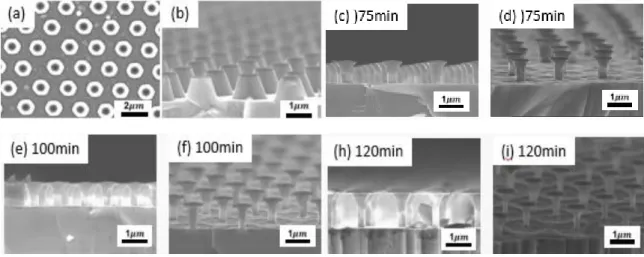
If we compare the results by using silica nanospheres and nanodisks fabricated using NLL, we can summarized the differences between these two results. First, the silica nanospheres method is round and smooth reflecting to the quality of the outlook of the nanospheres. The metal disk method is usually not as smooth and round especially when the disk diameter is very small. However, the commercially available silica nanospheres are rather limited, which also limits the attainable diameter of the nanorods. We can fabricate nanodisks with various disk diameters by adjusting the exposure diameters. So we can continuously tune the diameter of the nanorods. Besides, the high etch selectivity of metal hard mask is also good to fabricate nanorod with very small diameters.
Fig. 6. Using silica nanospheres as the hard mask:
After dry ICP etch of 1μm:(a) Cross-section (b) Top-view SEM image, After wet etch of different etch durations:
(c)(d) 75min (e)(f)100min (h)(i)120min
Figure 6(b) shows clearly observed that the round metal nanodisk will result in cone-shaped nanorods arrays after dry ICP etch. The additional wet etch will smooth the sidewall and change the outlook of the nanorods. As you can observe in the SEM images of nanorods after 75 mins to 120 mins of wet etch, the mushroom-like shape nanorods gradually appear. The etch rate of p-GaN is slower than the n-GaN. The diameter for the nanorods before the wet etch is about 1micron for the n-GaN and 800 nm for the p-GaN. After 120 nm wet etch, the diameter become 200 nm for the n-GaN and 500 nm for the p-GaN.
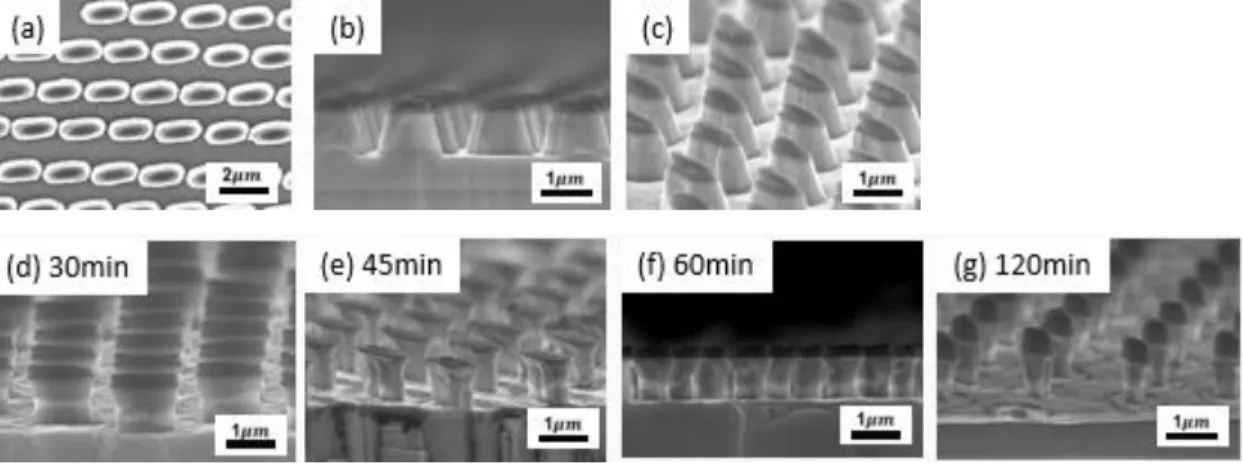
If we use the fabricated nano-ellipse as the hard mask during the ICP dry etch, we can fabricate elliptical nanorods after dry etch, which can be observed in the SEM images. The etch depth is around 1 micron. After ICP etch, the long axis of the p-GaN region is about 1300 nm and the n-GaN is about 1000 nm. After the wet etch, the length of the long and short axes both become smaller. The minimum length of the long axis we obtained in this study is about 660 nm for the p-GaN and 400 nm for the n-GaN. The length of the short axis after ICP etch is around 430 nm for the p-GaN and 380 nm for the n-GaN. The wet etch reduces the length of the short axis to 290 nm for the p-GaN and 160 nm for the n-GaN. Although we can fabricate elliptical shape nanorods using this method, the wet etch apparently does not result in smooth vertical surface.
Since we can fabricate a short axis for as short as 160 nm for the n-GaN, it is very possible that the light emission from the multiple quantum wells is highly polarized. We will perform new optical characteristics, such as CL or PL
to test polarization status of the fluorescent properties.
Fig. 7. Using metallic nano-ellipse arrays fabricated by using NLL as the hard mask:
After dry ICP etch of 1μm:(a) Top-view (b)(c) Cross-section SEM image, After wet etch of different etch durations:
(d) 30min (e)45min (f)60min (g)120min
Fig. 8. The CL spectrum In order to understand the optical properties of these nanoscale nanorod LED, we have performed CL
measurements with the help from Prof. Tu’s research group in Sun Yet-sen University in Kaohsiung, Taiwan. The CL spectrum reveals two distinct response. The 370 nm peak corresponds to the PL from GaN and the 450 nm
corresponds to the emission from the multiple quantum wells.
For two-step etch using silica nanospheres, the diameter of the p-GaN is between 725 nm to 392 nm. The diameter of n-GaN is between 950 nm to 150 nm. The size is controlled by the silica nanospheres used in the experiment. We also found out that the ITO layer will not be etched during the wet-etch process.
Fig. 9. (a)The 370 nm mono-CL images have revealed a higher intensity at the surface and the bottom of the nanorods, which both correspond to the GaN region. (b)The 440 nm mono-CL images reveal high emission responses only at the quantum well region. The quantum well is located at a depth of 180 nm from the p-GaN surface.
Conclusion:
In conclusion, we have demonstrate the ability to fabricate round and elliptical nanorod LEDs using the two- steps etch method. The etch hard mask can be fabricated with Nanospherical-Lens lithography developed in our lab. The size of the hard mask can be widely tuned by varying the exposure parameters.
449nm 370nm
(a) (b)
For two-step etch using silica nanospheres, the diameter of the p-GaN is between 725 nm to 392 nm. The diameter of n-GaN is between 950 nm to 150 nm. The size is controlled by the silica nanospheres used in the experiment. We also found out that the ITO layer will not be etched during the wet-etch process.
For hard mask fabricated using NLL, we can fabricate round and elliptical nanorods after two-step etch processes.
We can control the exposure parameters to tune the initial diameters of the nanorods. We can further control the diameters after various wet etch durations. The minimum diameter of the nanorod LED is as narrow as 200 nm in the n-GaN region. The minimum length of short axis for the elliptical nanorod is around 170 nm. These are very small LED samples that are aligned vertically on the substrate.
Next, we have test to perform the CL measurement from the fabricated nanorod LEDs and the CL images confirms the light emission from the MQW region.
References:
1. Yun-Chorng Chang, Sih-Chen Lu, Hsin-Chan Chung, Shih-Ming Wang, Tzung-Da Tsai & Tzung-Fang Guo, “High-Throughput Nanofabrication of Infra-red and Chiral Metamaterials using Nanospherical-Lens Lithography”,SCIENTIFIC REPORTS,3 : 3339, DOI: 10.1038/srep03339
2. Yun-Chorng Chang, Jyun-Sen Huang, and Hsin-Chan Chung, “Controlled fabrication of photonic crystals in situ using nanospherical-lens lithography”, SPIE Newsroom, 10.1117/2.1201203.004163
3. Qiming Li,1 Karl R. Westlake,1 Mary H. Crawford,1 Stephen R. Lee,1 Daniel D. Koleske,1 Jeffery J. Figiel,1 Karen C. Cross,1 Saeed Fathololoumi,2 Zetian Mi,2 and George T. Wang1, “Optical performance of top-down fabricated InGaN/GaN nanorod light emitting diode arrays”, OPTICS EXPRESS, Vol. 19, No. 25.