C.J. Liu and J.S. Chena)
Department of Materials Science and Engineering, National Cheng Kung University, Tainan, Taiwan 701, Republic of China
(Received 20 May 2004; accepted 23 November 2004)
In this work, the microstructure and oxidation resistance of pure Cu, Cu(0.2 at.% Zr) and Cu(2.5 at.% Zr) alloy films deposited on SiO2/Si by sputtering were explored. Upon annealing, the Zr additives diffused to the free surface and reacted with the residual oxygen in the vacuum system. An additional ZrO2 layer formed and covered the Cu(2.5 at.% Zr) film surface after annealing at 700 °C for 30 min. Simultaneously, of the three films, the Cu(2.5 at.% Zr) film exhibited the highest degree of Cu(111) preferred orientation and the lowest degree of void growth upon annealing.
Additionally, the Cu(2.5 at.% Zr) film pre-annealed at 700 °C showed a superior oxidation resistance when annealed at 200 °C in air for 15 min. Microstructure and oxidation resistance of Cu(Zr) alloy films were clearly affected by the ZrO2layer formed via the segregation of Zr additives, and the connection is discussed.
I. INTRODUCTION
Over the past decade, high performance on-chip inter-connects for multilevel metallization of ultralarge scale integration (ULSI) circuits has been extensively investi-gated and developed. Due to the continuous down-scaling of device dimensions, improvement on the resis-tance capaciresis-tance (RC) time delay of interconnects be-comes an essential issue. To reduce the RC delay, copper is the most promising candidate because of its low resis-tivity (∼1.7 ⍀ cm for bulk) and higher electromigration resistance than the conventional Al-based interconnects.1 However, there are several major drawbacks in the presence of Cu interconnects. One of the most important technical problems for Cu interconnects is the passiva-tion of exposed Cu against oxidapassiva-tion. Unlike the oxida-tion of Al, the oxidaoxida-tion rate of Cu is fast, and the oxide layer formed on Cu surface is not self-passivating. Thus, it cannot prevent further oxidation on the Cu surface. As a consequence, Cu is likely to oxidize during processing due to this deficiency.2
In addition, a thin Cu layer is easy oxidized in air around 250 °C. The formation of oxide degrades the electric property of Cu.3
Therefore, oxida-tion of Cu is an important issue that needs to be ad-dressed. To avoid this problem, a capping layer is used to prevent Cu from oxidizing. However, this additional layer may either complicate the processes or increase the
overall resistance. Based on the limitation, the develop-ment of an alternative course may need to be created. Similar to the Al-based alloy, a novel scheme to circum-vent this problem is to alloy Cu with additive atoms.4,5
In this study, we investigated the difference of oxida-tion property between pure Cu and Cu–Zr alloy films [hereafter referred to as Cu(Zr)] with SiO2. Igarashi et al. reported that the median time to failure (MTF) of copper alloy containing 0.14 at.% of Zr was two orders of mag-nitude larger than that of pure Cu film.6 However, the main drawback such as oxidation property has not been addressed. In addition, the different microstructures be-tween pure Cu and Cu(Zr) films have not been thor-oughly studied yet. The microstructure of the copper in-terconnection, such as grain size and its distribution, as well as texture, is an important issue because it will criti-cally influence the device performance and reliability.7 In this study, pure Cu and two kinds of Cu(Zr) alloy thin films were deposited on SiO2/〈Si〉 substrates (〈Si〉 repre-sents the single crystal wafer) and subsequently an-nealed. The objective of this work was to investigate the effect of adding Zr additive on the microstructural evo-lution and oxidation resistance of the Cu film. The sur-face reactions of Cu(Zr) thin films were also studied.
II. EXPERIMENTAL PROCEDURES
Phosphorus-doped n-type silicon (100) wafers with a thermally grown SiO2layer (270 nm) were used as sub-strates in the experiments. Pure Cu and two kinds of Cu(Zr) alloy films were deposited onto the substrates by magnetron sputtering. The Cu alloy films were prepared
a)
Address all correspondence to this author. e-mail: [email protected] DOI: 10.1557/JMR.2005.0068
by co-sputtering from a Cu target (99.99% purity) and a Zr target (99.2% purity) in Ar gas and at a negative substrate bias of 150 V. The base pressure of the chamber was 2.5 × 10⁻⁶
Torr, and the working pressure was 4 mTorr. The Zr additive contents of the two Cu(Zr) alloy films investigated in this work were determined by an electron probe microanalyzer (EPMA; JEOL 8900R, Peabody, MD) to be 0.2 at.% [referred to as Cu(0.2 at.% Zr)] and 2.5 at.% [referred to as Cu(2.5 at.% Zr)]. The thicknesses of pure Cu and both Cu(Zr) alloy films were measured by a profilometer (TENCOR␣-step, San Jose, CA), and they are 180 and 150 nm, respectively. After deposition, all samples were annealed in vacuum (to-gether with Ti foils to reduce residual oxygen) at a pres-sure of 2 × 10⁻⁵Torr. The annealing temperature was in the range of 500 to 800 °C, and the duration was 30 min. In addition, for the oxidation test, all samples were an-nealed at 200 °C in air for 5 to 15 min.
After deposition and annealing, the compositional depth profile analysis was performed by using Ruther-ford backscattering spectrometry (RBS) with 2 MeV He+ beams, and the scattering angle of detected particles at 160°. The chemical state of surface was monitored using x-ray photoelectron spectroscopy (XPS; VG ESCA 210, West Sussex, UK) with Al K␣radiation. The character-istic phases in the samples were identified by using-2 x-ray diffraction (-2 XRD; RIGAKU D-Max-IV, Osaka, Japan) and glancing incident angle c-ray diffrac-tion (GIAXRD; RIGAKU DMAX 2500) with Cu K␣ radiation. Surface morphology was revealed with scan-ning electron microscopy (SEM; PHILIPS XL-40FEG, Eindhoven, The Netherlands) operating at 15 kV, and the images were formed by collecting secondary electrons. The grain microstructure of the films was observed by transmission electron microscopy (TEM; HITACHI HF-200, Tokyo, Japan) operating at 200 kV. The TEM mi-crographs investigated in this study are bright-field (BF) images, which are formed when the objective aperture is positioned to pass the transmitted electrons contributing to the image. Plan-view TEM samples were prepared by thinning the Si substrate mechanically with sandpapers to about 20m. Afterward, the samples were further milled by Ar ions to electron transparency. Normalized sheet resistances of all samples were calculated from the sheet resistance measured with a four-point probe.
III. RESULTS AND DISCUSSION A. Additional layer on the surface
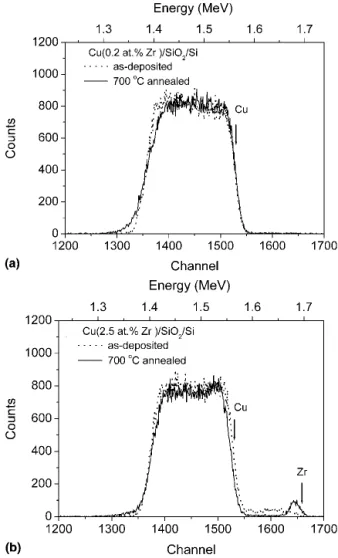
Figure 1 shows the RBS spectra of Cu(0.2 at.% Zr)/ SiO2/〈Si〉 and Cu(2.5 at.% Zr)/SiO2/〈Si〉 samples before and after annealing at 700 °C. The Zr signals are ob-served in the spectra of both as-deposited and 700 °C annealed Cu(2.5 at.% Zr) samples [Fig. 1(b)] but not seen in the as-deposited and annealed Cu(0.2 at.% Zr) samples
[Fig. 1(a)]. The reason for the absence of Zr signal for the Cu(0.2 at.% Zr) system should be attributed to the low Zr content. However, compared to the spectrum of as-deposited Cu(2.5 at.% Zr)/SiO2/〈Si〉 sample, an enhanced Zr peak from the sample surface is seen in the spectrum of 700 °C annealed Cu(2.5 at.% Zr)/SiO2/〈Si〉. This result indicates that a major part of added Zr atoms in the Cu film diffuses to the free surface. This observation is rea-sonable since the Zr content substantially exceeds its solid solubility with Cu (which is∼0.1 at.% at 700 °C8). In addition, one can see that Cu signal of the Cu(2.5 at.% Zr) sample is shifted slightly to lower energies after an-nealing at 700 °C [Fig. 1(b)]. On the contrary, the Cu profiles of as-deposited and annealed Cu(0.2 at.% Zr) samples overlap nicely at the front edge [Fig. 1(a)]. This result indicates that an additional layer covers on the Cu(2.5 at.% Zr) film after annealing at 700 °C. This layer consists of ZrO2 as will be revealed by examining the Cu(2.5 at.% Zr) surface using XPS analysis (see next section). The Zr additives in the Cu(0.2 at.% Zr) film FIG. 1. 2 MeV He+Rutherford backscattering spectra of (a) Cu(0.2 at.% Zr)/SiO2/〈Si〉and (b) Cu(2.5 at.% Zr)/ SiO2/〈Si〉 samples, before
and after vacuum annealing at 700 °C for 30 min. Surface scattering energies of Cu and Zr are indicated with arrows.
should also diffuse to the free surface upon annealing; however, the quantity may be too small to form an ad-ditional layer.
B. Chemical state of the surface
Figure 2 shows the XPS spectra of Zr 3d core lev-els obtained from the surface of Cu(0.2 at.% Zr) and Cu(2.5 at.% Zr) film, as-deposited and after annealing at 700 °C in vacuum. The Zr signal was observed on the surface of both as-deposited and annealed Cu(2.5 at.% Zr) films [Fig. 2(b)], but not seen in the as-deposited and annealed Cu(0.2 at.% Zr) films [Fig. 2(a)]. Again, the absence of Zr signal for the Cu(0.2 at.% Zr) system should be attributed to the low Zr content. The Zr 3d5/2 peaks (low-energy branch of the doublet) are at 181.2 and 181.8 eV for the as-deposited and annealed Cu(2.5 at.% Zr) films, respectively. It has been reported that the Zr 3d5/2 peak positions of ZrO2 and metallic Zr are 181.99and 178.9 eV.10Therefore, the bonding state of Zr for as-deposited and annealed Cu(2.5 at.% Zr) films should be corresponding to ZrOx (x < 2, incompletely
oxidized Zr) and ZrO2, respectively. However, the inten-sity of Zr signal on the surface of annealed Cu(2.5 at.% Zr) film is much greater than that of the as-deposited Cu(2.5 at.% Zr) film [Fig. 2(b)]. Formation of the
Zr oxide may be attributed to the reaction of out-diffused Zr additives with residual O2 during sputtering or in the vacuum furnace. This observation is reasonable since Zr is more reactive with O2 than Cu.
11
Therefore, the Zr additives of annealed Cu(2.5 at.% Zr)/SiO2/〈Si〉 sample would be driven to the film surface to form Zr oxide. This self-grown ZrO2 layer on the surface of the Cu(2.5 at.% Zr) film may have an effect on the re-tardation of Cu oxidation. The hypothesis will be proven by examining the oxidation resistance of Cu(2.5 at.% Zr) films in comparison with that of pure Cu films, which is discussed in the Sec. III. D.
C. Microstuctural evolution
The analytical techniques to convey the microstruc-tural evolution include -2 XRD, SEM, and TEM. Figure 3 shows the -2 XRD patterns of pure Cu, Cu(0.2 at.% Zr), and Cu(2.5 at.% Zr) samples, before and after annealing at 500–800 °C in vacuum. The patterns of as-deposited Cu(0.2 at.% Zr)/SiO2/〈Si〉 and Cu(2.5 at.% Zr)/SiO2/〈Si〉 samples exhibit Cu diffraction peaks only. However, compared to the pattern of as-deposited Cu sample, the position of Cu(111) peaks of Cu(2.5 at.% Zr) sample shifts to a lower angle, which may be due to the existence of Zr additive in Cu, resulting in the ex-pansion of Cu lattice. A similar result has been reported in our pervious Cu(Ta) study.12 After annealing, the Cu(111) peak of Cu(2.5 at.% Zr) films approaches that of pure Cu films. This result indicates that the lattice spac-ing of annealed Cu(2.5 at.% Zr) films is similar to that of pure Cu films. It is reasonable because the Zr additives had segregated to surface upon annealing, as revealed by the RBS and XPS analyses.
The degree of Cu(111) texture can be evaluated from the intensity ratios of Cu(111) peak to Cu(200) peak (I111/I200). The I111/I200 ratios of Cu and Cu(Zr) films increase after annealing. At the highest annealing tem-perature (800 °C), the I111/I200ratios for pure Cu, Cu(0.2 at.% Zr), and Cu(2.5 at.% Zr) films are about 11, 15 and 35, respectively. From the results, we realize that the degree of Cu (111) preferred orientation (the I111/I200 ratio) increases with increasing Zr alloy content in Cu and the I111/I200 ratio of Cu(2.5 at.% Zr)/SiO2/〈Si〉 sample is significantly larger than the other two. Obser-vation of Cu (111) preferred orientation for annealed pure Cu and Cu(Zr) films is expected because (111) planes of the face-centered-cubic (fcc) lattice possess the minimum surface energy.13With high Zr content, a sub-stantial strain energy develops in the Cu(Zr) alloy film because of the large mismatch of atomic radii between Cu and Zr (1.28 Å for Cu and 1.60 Å for Zr in 12-coordinated metals).14 Consequently, a strong Cu(111) texture is formed in the Cu(2.5 at.% Zr) film to reduce the overall energy. Ryu et al.15
had reported that FIG. 2. X-ray photoelectron spectra of Zr 3d core levels obtained from
the surface of as-deposited and 700 °C annealed (a) Cu(0.2 at.% Zr)/ SiO2/〈Si〉and (b) Cu(2.5 at.% Zr)/SiO2/〈Si〉 samples.
electromigration resistance of Cu can be improved realizing a high orientation of Cu(111) film on a SiO2 -based dielectric layer. In addition, Wong et al.16 had reported that a strong Cu(111) can enhance the adhesion between the Cu seed layer and diffusion barrier. From these points of view, increasing the intensity ratio of Cu(111) peak to Cu(200) peak in the Cu(2.5 at.% Zr)/ SiO2/〈Si〉 system can be beneficial for the performance of Cu interconnect.
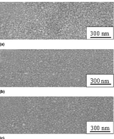
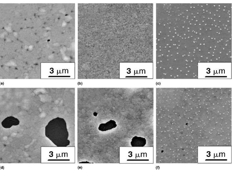
SEM micrographs on the surfaces of the as-deposited Cu/SiO2/〈Si〉, Cu(0.2 at.% Zr)/SiO2/〈Si〉, and Cu(2.5 at.% Zr)/SiO2/〈Si〉 systems are shown in Fig. 4. There is no significant difference in the surface morphology of the three as-deposited samples. Figure 5 shows the SEM micro-graphs on the surfaces of Cu/SiO2/〈Si〉, Cu(0.2 at.% Zr)/ SiO2/〈Si〉, and Cu(2.5 at.% Zr)/SiO2/ 〈Si〉 samples after annealing at 700 and 800 °C. After annealing at 700 °C, microvoids are seen on the surface of the 700 °C annealed Cu film [Fig. 5(a)]. However, no voids are ob-served on both the surfaces of the 700 °C annealed Cu(0.2 at.% Zr) and Cu(2.5 at.% Zr) films [Figs. 5(b) and 5(c)]. After annealing at 800 °C, microvoids of Cu and Cu(0.2 at.% Zr) films [Figs. 5(d) and 5(e)] are evident and coalesce to macrovoids, which clearly exposes the SiO2substrate. However, surface morphology of 800 °C annealed Cu(2.5 at.% Zr) film is still smooth although microvoids are seen [Fig. 5(f)]. From the SEM results mentioned above, we realize that the size of voids de-creases with increasing the Zr content in Cu.
It is apparent that additional precipitates were ob-served and uniformly scattered on the surface of annealed Cu(2.5 at.% Zr) film [Figs. 5(c) and 5(f)]. Compared to the as-deposited Cu(2.5 at.% Zr) film, the chemical com-position of the Cu matrix and precipitates for the annealed Cu(2.5 at.% Zr) film are both rich in Zr as
FIG. 3. -2 XRD patterns of (a) Cu/SiO2/〈Si〉, (b) Cu(0.2 at.%
Zr)/ SiO2/〈Si〉, and (c) Cu(2.5 at.% Zr)/ SiO2/〈Si〉 samples, before and
after annealing at 600, 700, and 800 °C. The dash-dot line indicates the Cu(111) peak position of the pure Cu film, which is only 0.08° devi-ated from the ICDDPDF (04-0836) data.
FIG. 4. Scanning electron micrographs on the surfaces of as-deposited (a) Cu/SiO2/〈Si〉, (b) Cu(0.2 at.% Zr)/ SiO2/〈Si〉, and (c) Cu(2.5 at.%
investigated by spot-Auger electron spectroscopy analysis (beam size ⳱ 300 nm). However, the Zr con-tent of these precipitates is higher than that of Cu ma-trix. As mentioned above, we realized that the Zr additives of annealed Cu(2.5 at.% Zr) film were segre-gated to the free surface, as revealed by RBS and XPS results.
To understand the difference of grain sizes between pure Cu and Cu(2.5 at.% Zr) films, the planar-view TEM micrographs of as-deposited and 700 °C annealed Cu(2.5 at.% Zr), as well as 700 °C annealed pure Cu films, were obtained as shown in Fig. 6. Because granu-lar structures can be seen in the micrographs, we have estimated the grain size from these bright-field TEM im-ages without using the dark-field TEM imim-ages. The mean grain size was determined by the line intercept method.17 Obviously, compared to the as-deposited Cu(2.5 at.% Zr) film [Fig 6 (a)], the grains of 700 °C annealed Cu(2.5 at.% Zr) film had grown in size. The grain sizes of Cu(2.5 at.% Zr) films, as-deposited and after annealing at 700 °C, are about 30 and 200 nm, respectively. However, the grain sizes of 700 °C annealed pure Cu film [Fig. 6(c)] is
significantly large, which is about 400 nm in average. The average grain size of the 700 °C annealed Cu(2.5 at.% Zr) film is only half of the pure Cu grain size. Compared to the pure Cu system, the low degree of grain growth for the Cu(2.5 at.% Zr) system can be attributed to the two factors. First, the Zr additives segregate to the grain boundaries, which inhibit the movement of grain bound-aries. Since Zr has a very limited solid solubility in Cu,8 theoretically, Zr atoms should segregate to the grain boundaries. This phenomenon has been reported by Iga-rashi et al.6They reported that for the Cu(1.4 at.% Zr) film, the Zr additives would segregate to the grain bound-aries after annealing in vacuum for 5 min. Second, the transmission of mass in the Cu surface and the movement of grain boundary would be restricted by a capping layer.18As mentioned in the RBS and XPS results, the Zr additives would diffuse out to the Cu(2.5 at.% Zr) film surface to form an additional ZrO2layer after annealing. This layer may act as the capping layer to inhibit grain growth of Cu upon annealing.
According to the SEM and TEM results mentioned above, we realize that the formation and growth of voids FIG. 5. Scanning electron micrographs on the surfaces of 700 °C annealed (a) Cu/SiO2/〈Si〉, (b) Cu(0.2 at.% Zr)/SiO2/〈Si〉, (c) Cu(2.5 at.%
is related to the degree of grain growth. The formation and growth of the voids indicate the initiation of copper agglomeration,19
which should be due to the grain growth of Cu during annealing. In addition to the void growth accompanied to the grain growth, the existence of residual tensile stress in the film is another factor that influences the void growth after the heating-and-cooling process.20 Residual tensile stress is generated during heating-and-cooling process due to the different coeffi-cients of thermal expansion (CTE) between the film and the substrate. However, in the current study, the CTE of pure Cu and Cu(Zr) films should be comparable due to low Zr content in the Cu. As a result, the discrepancy in the CTE of all films should be negligible when the samples were annealed at a specific temperature under the same heating-and-cooling processes. Because the void growth of annealed Cu and Cu(Zr) films (Fig. 5) is quite different, grain growth shall have the major infer-ence on the void growth.
As a result, since the degree of formation and growth of voids, as well as the grain growth of Cu(Zr) film is less than that of pure Cu film, adding Zr additives in Cu film to form the self-grown ZrO2 layer on the Cu(Zr) film surface will inhibit the copper agglomeration during annealing.
D. Oxidation-resistance analysis
The analytical techniques to examine the difference of oxidation resistance between Cu and Cu(2.5 at.% Zr) films are GIAXRD and normalized sheet resistance measurement. All samples were annealed at 200 °C for 5–15 min in air. However, some of Cu(2.5 at.% Zr) samples were first annealed at 700 °C for 30 min in vacuum to form the self-grown ZrO2layer on the surface to investigate whether this layer can prevent the Cu from oxidizing. These Cu(2.5 at.% Zr) samples, which are annealed at 700 °C in vacuum before oxidation, were referred to as pre-annealed Cu(2.5 at.% Zr) samples here-after. Figure 7 shows the GIAXRD patterns of pure Cu, Cu(2.5 at.% Zr) and pre-annealed Cu(2.5 at.% Zr) samples, as prepared (as deposited or right after pre-annealing) and after oxidizing at 200 °C in air for various time durations. All as-prepared samples show only a Cu diffraction peak. After the oxidation test, additional Cu2O diffraction peaks are observed in the XRD pat-terns of pure Cu and Cu(2.5 at.% Zr) samples [Figs. 7(a) and 7(b)]. This result indicates that both pure Cu and Cu(2.5 at.% Zr) samples have been oxidized after the oxidation test. It is well known that the oxidation of Cu easily occurs at low temperatures.3However, compared to the pure Cu sample, the intensity of Cu2O diffraction peaks for Cu(2.5 at.% Zr) is weaker [Fig. 7(b)]. This suggests that the degree of Cu oxidation of Cu(2.5 at.% Zr) sample is lower than that of pure Cu sample. Never-theless, the intensities of Cu2O diffraction peak for pure Cu and Cu(2.5 at.% Zr) samples increase with increasing oxidation time [Figs. 7(a) and 7(b)]. This result indicates that the degree of oxidation of these two systems in-creases upon increasing the annealing time. A similar result has been reported by Ding et al.21 They reported that the thickness of Cu oxide for pure Cu samples, after annealing in air, increases with increasing the oxidation time. For the pre-annealed Cu(2.5 at.% Zr) system, in addition to Cu peak, a diffraction peak pertaining to te-tragonal ZrO2(ICDDPDF 50-1089)
22
was observed be-fore and after oxidation test [Fig. 7(c)]. It should be associated with the self-grown ZrO2layer located on the surface after annealing at 700 °C for 30 min in vacuum, as revealed by XPS. However, no diffraction peaks cor-responding to Cu2O are observed after oxidation. It in-dicates that the pre-annealed Cu(2.5 at.% Zr) samples are not oxidized when annealing at 200 °C in air, for as long as 15 min. Reduction of Cu oxidation can be attributed to the formation of ZrO2 layer to prevent the oxidation of Cu.
Figure 8 shows the normalized sheet resistance of pure Cu, Cu(2.5 at.% Zr) and pre-annealed Cu(2.5 at.% Zr) films before and after annealing at 200 °C in air for 5–15 min. The normalized sheet resistance of the film is giv-en by
FIG. 6. Planar-view transmission electron micrographs of (a) as-deposited Cu(2.5 at.% Zr)/SiO2/〈Si〉, (b) 700 °C annealed Cu(2.5 at.%
⌬RsⲐRs0= 共Rs− Rs0兲ⲐRs0 ,
where Rs0and Rs, respectively, are the initial value and final value of sheet resistance. The normalized sheet re-sistance of pure Cu and Cu(2.5 at.% Zr) films increases dramatically after oxidation test. It indicates that they are oxidized as expected. However, the normalized sheet resistances of various pre-annealed Cu(2.5 at.% Zr)
films are almost the same after oxidation. This result indicates that the degree of Cu oxidation for pre-annealed Cu(2.5 at.% Zr) films is significantly lessened in com-parison with the Cu and Cu(2.5 at.% Zr) films. This result is consistent with the GIAXRD result. A similar result has also been reported by Li et al.23
They reported that the normalized sheet resistance of Cu(35 at.% Ti) film measured by the in situ method is much small than that of pure Cu film after annealing from room tempera-ture to 200 °C (the heating rate is 2 °C/min). From the oxidation resistance result mentioned above, we realize that the self-grown ZrO2 layer on the surface of pre-annealed Cu(2.5 at.% Zr) film plays an important role in inhibiting the oxidation of Cu.
IV. CONCLUSION
In this work, the microstructure and oxidation resis-tance of Cu/SiO2/〈Si〉, Cu(0.2 at.% Zr)/SiO2/ 〈Si〉, and Cu(2.5 at.% Zr)/SiO2/〈Si〉 samples were studied. A self-grown ZrO2layer is observed on the surface of 700 °C annealed Cu(2.5 at.% Zr) film due to the reaction of out-diffused Zr additives with residual O2, during sput-tering or post-deposition annealing in vacuum. This layer serves as a capping layer to inhibit the formation and growth of the voids during annealing. In addition, the ZrO2layer can prevent oxidation of Cu in air at 200 °C. Therefore, alloying Zr atoms in Cu will improve the mi-crostructure and oxidation resistance of Cu. However, the Zr concentration needs to be substantial (2.5 at.% in this study) for forming a self-grown ZrO2 passivation layer, so that these advantages can be revealed.
ACKNOWLEDGMENT
The authors gratefully acknowledge the financial sup-port from the National Science Council of Taiwan, Re-public of China (Grant No. NSC-92-2216-E-006-022). FIG. 7. GIAXRD patterns of (a) Cu/SiO2/〈Si〉, (b) Cu(2.5 at.%
Zr)/SiO2/〈Si〉, and (c) pre-annealed Cu(2.5 at.% Zr)/SiO2/〈Si〉 samples,
before and after oxidizing in air at 200 °C for 5, 10, and 15 min.
FIG. 8. Normalized sheet resistance values as a function of oxidation time at 200 °C in air for pure Cu, Cu(2.5 at.% Zr), and pre-annealed Cu(2.5 at.% Zr) films.
REFERENCES
1. S.P. Murarka: Multilevel interconnections for ULSI and GSI. Mater. Sci. Eng. R. 19, 87 (1997).
2. J. Li, G. Vizkelethy, P. Revesz, J.W. Mayer, and K.N. Tu: Oxida-tion and reducOxida-tion of copper oxide thin films. J. Appl. Phys. 69, 1020 (1991).
3. H.K. Lious, J.S. Huang, and K.N. Tu: Oxidation of Cu and Cu3Ge
thin film. J. Appl. Phys. 77, 5443 (1995).
4. W.A. Lanford, P.J. Ding, W. Wang, S. Hymes, and S.P. Muraka: Low-temperature passivation of copper. Thin Solid Films 262, 234 (1995).
5. W. Lee, H. Cho, B. Cho, J. Kim, Y.S. Kim, W.G. Jung, H. Kwon, J. Lee, P.J. Reucroft, C. Lee, and J. Lee: Factors affecting passi-vation of Cu(Mg) Alloy films. J. Electrochem. Soc. 147, 3066 (2000).
6. Y. Igarashi and T. Ito: Electromigration properties of copper-zirconium alloy interconnects. J. Vac. Sci. Technol. B 16, 2745 (1998).
7. R. Rosenberg, D.C. Edelstein, C-K. Hu, and K.P. Rodbell: Copper metallization for high performance silicon technology. Annu. Rev. Mater. Sci. 30, 229 (2000).
8. D. Arias and J.P. Abriata: Binary Phase Diagrams, 2nd ed., edited by T.B. Massalski (ASM International, Materials Park, OH, 1990), p. 1511.
9. D. Majumdar and D. Chatterjee: X-ray photoelectron spectro-scopic studies on yttria, zirconia, and yttria-stabilized zirconia. J. Appl. Phys. 70, 988 (1991).
10. J.F. Moulder, W.F. Stickle, P.E. Sobol, and K.D. Bomben: Hand-book of X-ray Photoelectron Spectroscopy (Physical Electronics, Inc., Eden Prairie, MN, 1995), p. 108.
11. I. Barin: Thermochemical Data of Pure Substances, 3rd ed. (VCH, New York, 1995), pp. 1505, 1880.
12. C.J. Liu, J.S. Chen, and Y.K. Lin: Characterization of microstruc-ture, interfacial reaction and diffusion of immiscible Cu(Ta) alloy
thin film on SiO2at elevated temperature. J. Electrochem. Soc.
151,G18 (2004).
13. M. McLean and B. Gale: Surface energy anisotropy by an im-proved thermal grooving technique. Philos. Mag. 20, 1033 (1969). 14. C. Kittel: Introduction to Solid State Physics, 7th ed. (John Wiley
& Sons, New York, 1996), p. 78.
15. C. Ryu, A.L.S. Loke, T. Nogami, and S.S. Wong: Effect of texture on the electromigration of CVD copper. In Proceedings of 1997 IEEE International Reliability Physics Symposium, Denver, CO, edited by A.K. Goel, pp. 201–205.
16. S.S. Wong, C. Ryu, H. Lee, A.L.S. Loke, K.W. Kwon, S. Bhattacharya, R. Eaton, R. Faust, B. Mikkola, J. Mucha, and J. Ormando: Barrier/seed layer requirements for copper intercon-nects. In Proceedings of 1998 IEEE International Interconnect Technology Conference, edited by R.H. Havemann, 1998, pp.107–109.
17. ASTM Standard Designation E-112-82, Sec. 3, Vol. 03.03, 1984 Annual Book of ASTM Standards (ASTM, Philadelphia, PA, 1984), p.126.
18. S.Y. Lee, R.E. Hummel, and R.T. DeHoff: On the role of indium underlays in the prevention of thermal grooving in thin gold films. Thin Solid Films 149, 29 (1987).
19. K.T. Miller, F.F. Lange, and D.B. Marshell: The instability of polycrystalline thin films: Experiment and theory. J. Mater. Res.
5,151 (1990).
20. D. Weiss, O. Kraft, and E. Arzt: Grain-boundary voiding in self-passivated Cu–1 at.% Al alloy films on Si substrates. J. Mater. Res. 17, 1363 (2002).
21. P.J. Ding and W.A. Lanford: Oxidation resistant high conductivity copper films. Appl. Phys. Lett. 64, 2897 (1994).
22. International Center for Diffraction Data Powder Diffraction File (ICDDPDF) No. 50-1089).
23. J. Li, J.W. Mayer, and E.G. Colgan: Oxidation and protection in copper and copper alloy thin films. J. Appl. Phys. 70, 2820 (1991).