A 40-110 GHz High-Isolation CMOS Traveling-Wave
T/R Switch by Using Parallel Inductor
Wen-Chian Lai and Huey-Ru Chuang
Institute of Computer and Communication Engineering, Department of Electrical Engineering, National Cheng Kung University,, Tainan, Taiwan, R.O.C
Abstract—A 40-110 GHz SPDT T/R switch fabricated in 90 nm CMOS is presented. The traveling wave switch is used to obtain low insertion loss and wide operating bandwidth. To enhance the isolation performance, the parallel inductor is adopted. The insertion loss is improved with body-floating. The measurement results show that the insertion loss is lower than 4 dB and isolation is better than 21 dB. A very good isolation value higher than 56 dB at 109 GHz is achieved. The chip core size is 0.11 mm2.
Index Terms—90-nm, 40-110 GHz, CMOS, high-isolation T/R switch, millimeter-wave (MMW), traveling wave
I. INTRODUCTION
Recently, Millimeter-wave (MMW) communication systems have tremendous developing potential and have many applications such as wireless personal area network (WPAN) around 57 – 64 GHz, automotive radar applications at 77 GHz and MMW radars for medical imaging and gesture recognition at 94 GHz [1][2]. In a MMW RF transceiver, the transmitter/receiver (T/R) switches with low insertion loss, high isolation and high power handling are required. Many MMW T/R switches are implemented with low insertion loss and high isolation by GaAS, HEMT process technology[3][4]. With the fast developing of CMOS process, system-on-chip (SoC) applications become mainstream for cost saving and highly integrated systems. However, CMOS lossy substrate will be a challenge for the switch design.
In general, the traveling-wave concept T/R switch is desired for MMW application due to low insertion loss and wide bandwidth response. However, there is tradeoff between insertion loss and isolation for traveling wave switches. Usually, high isolation and low insertion loss response may not be able to achieve simultaneously with traveling wave structure. In [5], the series-shunt structure with high isolation by using leakage cancellation technique is presented. Furthermore, parallel-shunt inductors are adopted to cancel NMOS parasitic effect to enhance switch isolation [6].
In this work, the parallel-shunt inductor is proposed in the design of a 40-110 GHz traveling-wave SPDT T/R switch. The designed switch is fabricated using the 90 nm CMOS technology. A wide bandwidth response is obtained, and both of high-isolation and low insertion loss are achieved.
II. CIRCUIT DESIGN A.TRAVELING WAVE SPST DESIGN
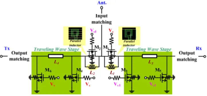
The circuit schematic of the proposed 40-110 GHz traveling wave SPDT T/R switch with the body-floating technique and parallel inductor is shown in Fig. 1. The T/R switch is designed
Fig. 1. Circuit schematic of the proposed 40-110 GHz high-isolation traveling wave T/R switch by using parallel inductor.
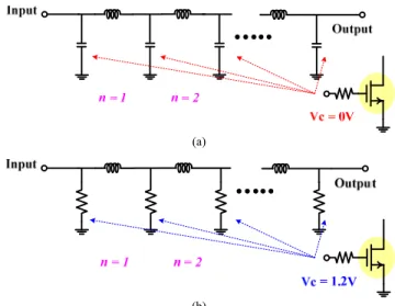
by applying two SPST traveling wave switches. The traveling wave stage can be designed by properly selecting the inductor’s value and transistor’s size, Fig. 2(a) shows the equivalent circuit of the SPST switch when the transistors are off-state. The characteristic impedance of the artificial transmission line is
off
C
L
Z
0
(1)Coff is the off-state capacitance of the transistors(M3-M6). In the
proposed switch design, L3,L4 is chosen as 60 pH and
transistors’ width (M3-M6) are chosen as 26 um.
For the SPST switch isolation, Fig. 2(b) shows the equivalent circuit when the transistors are on-state. It can be observed that tansistors are equivalent to small resistors, and the SPST circuit is equivalent to a small resistance path. The simulated results of different traveling wave sections are shown in Fig. 3. It can be obsered that there is tradeoff between isolation and insertion loss. The more traveling wave sections (n), the better switch isolation performance can be obtained. However, the insertion loss is deteriorated by limited-Q inductors and transistor’s parasitic effect. Hence, the traveling wave stage numbers (n) will be carefully chosen and discussed in the following section
B.SPDT SWITCH SYNTHESIS
The SPDT traveling-wave switch employing the series switch is reported in [4]. In order to improve the isolation performance, the parallel inductors (L1,L2) is applied to series
switch (M1,M2). When the series switch (M1,M2) is in off-state,
the parasitic capacitance is resonated with parallel inductor at resonance frequency (f = 1 / 2π LC). Thus, the isolation response is improved. Moreover, the isolation can be further improved by increasing the traveling wave stage [4].
(a)
(b)
Fig. 2. (a) Traveling SPST switch with off-state transistors. (b) Traveling SPST switch with on-state transistors
. 0 10 20 30 40 50 60 70 80 90 100 110 Frequency (GHz) -5 -4 -3 -2 -1 0 In s e rt io n l o s s ( d B ) -40 -30 -20 -10 0 Is o la tio n ( d B ) Loss:n=2 Loss:n=3 Loss:n=4 Isolation:n=2 Isolation:n=3 Isolation:n=4
Fig. 3. Simulation results of SPST switch with different traveling wave sections (n) 40 50 60 70 80 90 100 110 Frequency (GHz) -70 -60 -50 -40 -30 -20 -10 0 Is o la ti o n ( d B )
Single resonated switch
Resonated switch with traveling wave,n=1 Resonated switch with traveling wave,n=2 Resonated switch with traveling wave,n=3 Resonated switch with traveling wave,n=4
Fig. 4. Simulation results of SPDT switch using parallel inductor with
different traveling wave sections (n)
When the transistors of traveling wave SPST switch are in on-state, the leakage signal is led to ground by mutiple shunt resistors. However, as mentioned above, the insertion loss is deteriorated with multiple traveling wave stages. Simulation results of SPDT switch using parallel inductor with different traveling wave sections (n) is shown in Fig. 4.. In considering the trade off between insertion loss and isoloation, the width of the series switch (M1,M2) is chosen as 36 um, the parallel
indutor is chosen as 154 pH and traveling wave SPST switch stage is chosen as n=2 at the resonating frequency of 109 GHz. In order to further improve insertion loss response, matching
40 50 60 70 80 90 100 110 Frequency (GHz) -35 -30 -25 -20 -15 -10 -5 0 R e tu rn a n d I n s e rt io n L o s s ( d B ) Simu._Insertion loss Simu._Return loss Meas._Insertion loss Meas._Return loss (a) 0 10 20 30 40 50 60 70 80 90 100 110 Frequency (GHz) -60 -50 -40 -30 -20 -10 0 Is o la ti o n ( d B ) Post-simu. Measurement (b)
Fig. 5. Simulated and measured results: (a) return loss and insertion loss,
(b) isolation -10 -5 0 5 10 15 Input power (dBm) -7 -6 -5 -4 -3 -2 In s e rt io n l o s s ( d B ) Measurement
Fig. 6. Measured IP1dB with different input power at 94 GHz.
-15 -10 -5 0 5 10 15 Input power (dBm) -60 -50 -40 -30 -20 -10 0 Is o la ti o n ( d B ) 94 GHz Post-simu. Measurement
Fig. 7. Simulated and measured isolation at different input power at 94-GHz
circuits are adopted to the antenna (Ant), transmitter (Tx) and receiver (Rx) ports. For size reduction, all the microstrip lines of matching networks are meandered. Also for EM coupling consideration, all circuit has been simulated by the full-wave HFSS EM simulators.
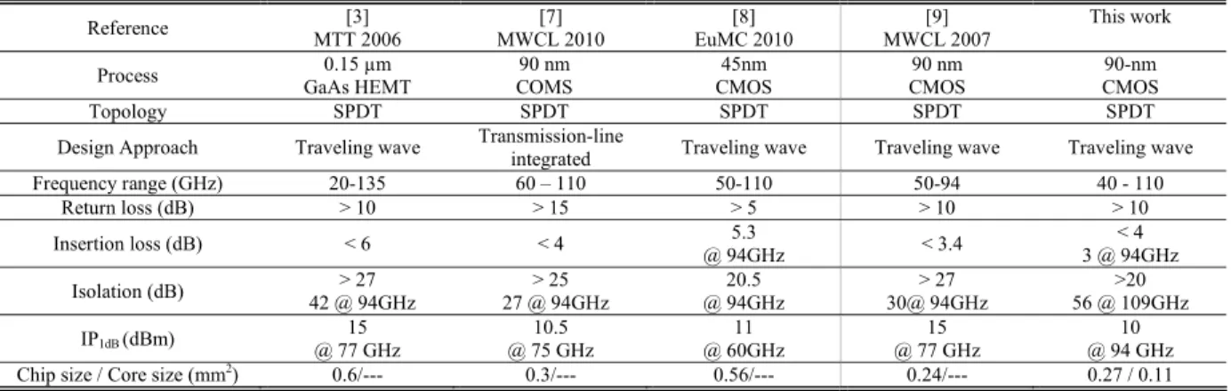
TABLE I PERFORMANCE COMPARISON Reference [3] MTT 2006 [7] MWCL 2010 [8] EuMC 2010 [9] MWCL 2007 This work
Process GaAs HEMT 0.15 µm COMS 90 nm CMOS 45nm CMOS 90 nm CMOS 90-nm
Topology SPDT SPDT SPDT SPDT SPDT
Design Approach Traveling wave Transmission-line
integrated Traveling wave Traveling wave Traveling wave
Frequency range (GHz) 20-135 60 – 110 50-110 50-94 40 - 110 Return loss (dB) > 10 > 15 > 5 > 10 > 10 Insertion loss (dB) < 6 < 4 5.3 @ 94GHz < 3.4 < 4 3 @ 94GHz Isolation (dB) 42 @ 94GHz > 27 27 @ 94GHz > 25 @ 94GHz 20.5 30@ 94GHz > 27 56 @ 109GHz >20 IP1dB (dBm) @ 77 GHz 15 @ 75 GHz 10.5 @ 60GHz 11 @ 77 GHz 15 @ 94 GHz 10
Chip size / Core size (mm2) 0.6/--- 0.3/--- 0.56/--- 0.24/--- 0.27 / 0.11
Fig. 8. Chip micrograph. (chip size= 0.27 mm2 and core size= 0.11 mm2)
III. MEASUREMENT RESULTS
The CMOS T/R switch is fabricated in the 90-nm CMOS process. As shown in Fig. 5(a), the insertion loss is lower than 4 dB, and the return loss is better than 10 dB, respectively. Fig. 5(b) shows that the isolation is better than 35 dB at 94 GHz and 56 dB at 109 GHz, respectively. Fig. 6 shows the measured IP1dB is 10 dBm at 94 GHz.
Furthermore, the isolation performance at different input power at 94 GHz has been investigated and shown in Fig. 7. The chip size of proposed SPDT switch is 0.27 mm2 and the
core size is 0.11 mm2. the chip micrograph is shown in Fig. 8.
Table I summarizes the measured performance comparison. Compared with reported MMW SPDT switches, the good high isolation performance of the proposed switch can be observed. The highest isolation value is 56 dB at 109 GHz. Also, a low insertion loss performance, which is less than 4 dB, is obtain without sacrificing other switch performance. The return loss are better than 10 dB. The input P1dB is 10
dBm at 94 GHz.
IV. CONCLUSION
A 40 - 110 GHz CMOS high-isolation traveling wave T/R switch by using parallel inductor is presented. The SPDT switch is fabricated in 90-nm CMOS technology. The body floating technique is adopted to achieve low insertion loss and high linearity. To achieve the high isolation performance, parallel-shunt inductors are employed. the measured results
show that the insertion loss can be less than 4 dB, and the return loss are better than 10 dB. The input P1dB is 10 dBm at
94 GHz. The isolation is better than 20 dB from 40 to 110 GHz, and the highest isolation value is 56 dB at 109 GHz. The switch chip size and core size is 0.27 mm2 and 0.11 mm2,
respectively.
ACKNOWLEDGEMENT
The authors would like to thank the Chip Implementation Center (CIC) of National Science Council and National Nano Device Laboratories (NDL), Taiwan, ROC, for supporting the TSMC CMOS process and chip measurement.
REFERENCES
[1] A. Arbabian, S. Callender, S. Kang, B. Afshar, J. –C. Chien, and A. M. Niknejad, “ A 90 GHz Hybrid Switching Pulsed-Transmitter for Medical Imaging,” IEEE J. Solid-State Circuits, vol. 45, no. 12, pp. 2667–2681, Dec 2010.
[2] A. Arbabian, S. Callender, S. Kang, M. Rangwala, and A. M. Niknejad, “A 94 GHz mm-Wave-to-Baseband Pulsed-Radar Transceiver with Applications in Imaging and Gesture Recognition,” IEEE J. Solid-State
Circuits, vol. 48, no. 4, pp. 1055–1071, Apr. 2013.
[3] Z. M. Tsai, M. C. Yeh, M. F. Lei, H. Y. Chang, C. S. Lin, and H. Wang, “FET-integrated CPW and the application in filter synthesis design method on traveling-wave switch above 100 GHz,” IEEE Trans.
Microw. Theory Tech., vol. 54, no. 5, pp. 2090–2097, May 2006.
[4] K.-Y. Lin, W.-H. Tu, P.-Y. Chen, H.-Y. Chang, H. Wang, and R.-B. Wu, “Millimeter-wave MMIC passive HEMT switches using traveling wave concept,” IEEE Trans. Microw. Theory Tech., vol. 52, no. 8, pp. 1798– 1808, Aug. 2004.
[5] C. –S. Kuo, H. –C. Kuo, H. –R. Chuang, C. -Y Chen and T. –H. Huang “A High-Isolation 60GHz CMOS Transmit/Receive Switch,” in IEEE
Radio Freq. Integr. Circuits Symp. Dig., Jun. 2011, pp. 1–4.
[6] C.-Y. Ou, H.-R. Lin, H.-R. Chuang and T.-H. Huang, “A high-isolation high-linearity 24-GHz CMOS T/R switch in the 0.18-μm CMOS process,” in Eur. Microw. Conf., Sep. 2009, pp. 250–253.
[7] R.-B. Lai, J.-J. Kuo, and H. Wang, “A 60–110 GHz transmission-line integrated SPDT switch in 90 nm CMOS technology,” IEEE Microw.
Wireless Compon. Lett., vol. 20, no. 2, pp. 85–87, Feb. 2010.
[8] T. Quémerais, L. Moquillon, J.-M. Fournier1, and P. Benech, “A SPDT Switch in a standard 45 nm CMOS process for 94 GHz Applications,”.
in Eur. Microwave Conf., Sep. 2010, pp. 425 – 428
[9] S. F. Chao, H. Wang, C.-Y. Su, and J. G. J. Chern, “A 50 to 94-GHz CMOS SPDT switch using traveling-wave concept,” IEEE Microw.
Wireless Compon. Lett., vol. 17, no. 2, pp. 130–132, Feb. 2007
[10] F.-J. Huang and K.O, “A 0.5 μm CMOS T/R switch for 900-MHz wireless application,” IEEE J. Solid-State Circuits, vol. 36, no. 3, pp. 486-492, Mar. 2001.