The Cathode Current Efficiency of Flip-Chip Solder
Bump Plating
Kwang-Lung Lin
*
,z and Yeh-hsiu LiuDepartment of Materials Science and Engineering, National Cheng Kung University, Tainan, Taiwan 701 Flip chip solder bumps were produced on various bump pad dimensions by electroplating to investigate their current efficiency. The bump pad dimensions range from 60⫻ 60 m to 250 ⫻ 250 m. Bump heights are in the range of 80-150 m. The bump height achieved is very uniform across a 4 in. wafer. The growth of bump height follows a parabolic trend with respect to plating time. Experimental results showed that the cathode current efficiency increases with increasing pad size. The cathode current efficiency also increases with respect to plating time and approaches a constant level after 30 min of deposition.
© 2003 The Electrochemical Society. 关DOI: 10.1149/1.1589761兴 All rights reserved.
Manuscript submitted November 25, 2002; revised manuscript received February 11, 2003. Available electronically June 23, 2003.
The manufacture of solder bumps is an important step in flip-chip bonding technology. A solder bump structure consists of under bump metallurgy共UBM兲 and the top solder mass. The UBM can be produced by sputtering deposition, for instance, TiW/Cu, Cr/Cu,1,2 or by electroless deposition for the electroless nickel deposit.3-5 Pro-cesses available for producing the top solder mass include evapora-tion deposievapora-tion, stencil printing, and electroplating. In principle, these processes can all apply to the same UBM combinations, al-though each commercial process does have its characteristic struc-ture.
Electroplating is by far the most feasible process for enabling the production of a fine pitch bump pattern. Electroplating of solder bump is conducted in a rather complicated condition in which there could be thousands of tiny cathodes, the bump pad. The current distribution among the tiny cathodes determines the solder mass plated and thus the bump height uniformity. Bump height uniformity is of importance and is strictly required for achieving satisfactory bonding. The solder bump height uniformity can be monitored by the appropriate design of the electroplating cell.6 In addition to bump height uniformity, for application purposes the cathode cur-rent efficiency is also of importance. A high cathode curcur-rent effi-ciency is certainly preferable in light of cost concerns. There has been no discussion of the cathode current efficiency issue in the electroplating of solder bump. This present work investigated the variation of cathode current efficiency with respect to solder bump pad dimensions and bump pattern designs.
Experimental
The solder bump was produced on a Si wafer. The Si wafer was precleaned by degreasing sequentially with trichloroethylene, ac-etone, and isopropanol, followed by deoxidizing in a 10% HF solu-tion. The production sequence of the solder bump is presented in the flow diagram as shown in Fig. 1. The cleaned Si wafer was depos-ited sequentially with the multiplayer of Ta/TaCu/Cu using magne-tron sputter deposition. The thickness of each layer is around 500 nm. On top of the Cu layer was deposited an electroless nickel共EN兲 deposit of 5 m in thickness. A layer, 30 m thick, of positive photoresist was spin-coated on the Cu surface. The Cu pad produced after developing was then etched with a HNO3 solution prior to electroless Ni deposition. The electroless nickel solution7 consists of 87 g/L NiSO4•6H2O, 24 g/L Na2H2PO2•H2O, 30 g/L CH3COONa•3H2O, 2 g/L C3H4(OH兲共COOH)3•H2O, 4.1 g/L NaO2C3H4COONa•6H2O, and 0.0015 g/L Pb共CH3COO)2•3H2O. 63 Sn-37 Pb solder was electroplated on the EN layer for the desired period of time at a current density of 30 mA/cm2. The distance between the anode and cathode is 5.5 cm. The solder, 63 Sn-37 Pb, bump was electroplated on the EN deposit to the given thickness. Solder plating was conducted using a commercial electrolyte of
which the detailed composition was proprietory. The photoresist was removed with acetone after solder plating. The Cu films in the pitch areas were then etched off to reveal Si.
The bump pad dimensions investigated were 60, 80, 100, 150, and 250m. The bump patterns were arranged as a one-pad
dimen-*Electrochemical Society Active Member.
zE-mail: [email protected] Figure 1. The flow diagram of solder bump production sequence.
Journal of The Electrochemical Society, 150共8兲 C529-C532 共2003兲 0013-4651/2003/150共8兲/C529/4/$7.00 © The Electrochemical Society, Inc.
C529
sion on a wafer共one-pattern兲 or four-pad size 共four-pattern兲 on a wafer. The four-pattern arrangement was so arranged that each pad dimension was allocated in each quarter of the wafer. Reflow of the plated solder bump was conducted with the aid of flux. The reflow was conducted with an IR furnace under a protective atmosphere of 90% N2and 10% H2. The flux was activated at 175°C for 30 s prior to raising the temperature, at a controlled ramp speed, up to the desired reflow temperature. The peak reflow temperature was 230°C. The dwell time at the reflow temperature was 15 s. The bump height value was measured using a surface profile system, and is presented as the average value of the bumps on the diagonal of each chip.
Results and Discussion
Electroplating of a solder bump is a complicated process as the process involves the simultaneous deposition of thousands of solder bumps. It is of importance to produce a uniform bump height throughout the chip for a flip-chip bonding application. Bump height is proportional to the solder mass plated on each bump pad. The total solder mass deposited on each bump pad is governed by the current density passing through each bump pad. Accordingly, a uni-form current distribution is desired for producing uniuni-form bump
size. The current distribution during electroplating of the solder bump can be manipulated by a suitable design for the electroplating cell as discussed in a previous study.6The electroplating cell therein designed produced a uniform bump height in this present study as presented in Fig. 2 and 3. Chip 1-1 to chip 5-5 represents the diag-onal position on the chip on the upper left quarter of the wafer. These are used to represent the behavior on a wafer because of the symmetrical consideration. The bump height presented is the aver-age value of bumps located on the diagonal line of each chip. The results shown in Fig. 2 and 3 obviously delineate that the bump heights on the wafer of one pattern of 80 and 250 m are very uniform across the wafer. Bump height is related to the total mass deposited on the bump pad. The total solder mass deposited is a function of the total quantity of electricity applied to each bump pad. The electroplating cell applied in this work has been so designed as to give uniform current distribution through each bump pad. The efficacy of the cell design relies on the application of a mesh cath-ode and a suitable ratio between the electrcath-ode distance and the elec-trode area.6The bump height increases with respect to the increase in electroplating time as would be expected. It is also seen that the Figure 2. Solder bump heights produced on a one-pattern wafer with 80m
bump pad.
Figure 3. Solder bump heights produced on a one-pattern wafer with 250 m bump pad.
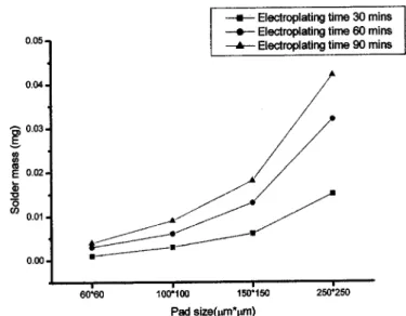
Figure 4. Solder mass deposited on a four-pattern wafer with four bump pad
dimensions on each wafer.
Figure 5. Solder mass deposited on a one-pattern wafer with a one pad
dimension on each wafer. Journal of The Electrochemical Society, 150共8兲 C529-C532 共2003兲
C530
250m pad achieved a greater bump height than 80 m pad for the same deposition time. This behavior is to be discussed further in the following.
The total solder mass deposited on a wafer may be estimated from the solder volume and solder density. However, it may raise the concern that the estimation accuracy of the bump mass, because the bump may not be exactly a spherical shape. This behavior is reflected by the results shown in Fig. 2 and 3. The solder bump shape and bump height is affected by the pad dimension and solder mass.8It is seen that Fig. 2 indicates the increase in bump height is only about 15m in between 30 and 60 min of deposition time. The wetting interaction between solder and bump pad, as well as the gravity effect, tends to lower the bump height. Accordingly, in view of the achievement of uniform bump height the estimation of cath-ode current efficiency is then performed by measuring the total mass deposited. The wafer was weighed prior to and after plating, and the solder mass deposited was obtained as the subtracted value.
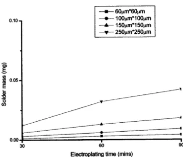
Figure 4 and 5 express the solder mass deposited on wafers of four-pattern and one-pattern arrangements, respectively. The solder mass presented is the mass of a single bump. The mass was obtained by dividing the weighed solder mass of a wafer by the total number of solder bumps. The four-pattern arrangement means the four-pad dimensions are produced on the same wafer, one on each quarter. Both pattern arrangements show an increase in solder mass with respect to the enlargement of bump pad dimensions. The variation of solder mass with respect to the bump pad dimension seems to have the same trend for all experiments. The presentation of the solder mass with respect to electroplating time, Fig. 6 and 7, indicates that Figure 6. Solder mass deposited on a four-pattern wafer with respect to
plating time.
Figure 7. Solder mass deposited on a one-pattern wafer with respect to
plating time.
Figure 8. The cathode current efficiency for solder bump plating on a
one-pattern wafer.
Figure 9. The metal ion concentration profile of the plating process. The
plating front moves and encounters different surface concentrations.
Journal of The Electrochemical Society, 150共8兲 C529-C532 共2003兲 C531
the solder mass increment does not follow a linear correlation with respect to electroplating time for both pattern arrangements in the period between 30 and 90 min. It is of interest to explore further the deposition behavior down to the very initial deposition period for current efficiency estimation. The mass accumulation within 30 min is not plotted separately. Instead, it is discussed as incorporated with the results of cathode current efficiency in the following.
The cathode current efficiency was calculated based on the Sn/Pb mass ratio of 63Sn-37Pb by assuming the reduction reactions
Sn⫹2⫹ 2e → Sn Pb⫹2⫹ 2e → Pb
To demonstrate this, the one-pattern wafer of bump pad dimension 150 m will have a total current of 151.875 ⫻ 10⫺3 A passing through the wafer when the current density is 30 mA/cm2. At an electroplating time of 90 min, the theoretical mass deposited is cal-culated as
where 74.81 and 25.19% are the mole percentages of Sn and Pb, respectively. The total mass⫽ MSn⫹ MPb⫽ 0.3774 ⫹ 0.2218 ⫽ 0.5992 g.
The cathode current efficiency is the ratio of the actual deposited mass to the theoretical mass calculated in the above-mentioned ex-ample. In view of the similarity in deposition behavior, Fig. 4 and 5, between different pattern arrangements, the discussion on current efficiency will simply focus on the one-pattern arrangement. The cathode current efficiency for the one-pattern arrangement for each pad dimension is presented in Fig. 8. The cathode current efficiency for each pad dimension increases with respect to electroplating time at the beginning 30 min of deposition. However, the cathode current efficiency reaches nearly a constant level after 30 min for each pad dimension. The constant level of cathode current efficiencies is be-tween 80 and 90%. The larger pad dimension possesses a greater cathode current efficiency during the whole deposition periods up to the end of 90 min.
The electrodeposition of the solder bump was conducted with the aid of photoresist to confine the bump pad opening. In the beginning of deposition, all the metal ions need to be guided to move into the openings. Considering the thickness, 30m, of the photoresist, it is believed that the diffusion of metal ions into the trench opening is restricted by the diffusion layer within which the metal ion concen-tration is relatively low compared to the bulk.9Accordingly, in the beginning of deposition, or soon after the deposition begins, the cathode current efficiency is expected to be low. The deficiency in surface concentration of metal ions can be improved by the pulse plating method which varies the diffusion layer thickness as well as the current distribution.10This present study did not apply the pulse current for plating. Accordingly, the diffusion layer profile remains constant throughout the plating process. The concentration profile within the trench opening can be viewed in Fig. 9. The progress of
electroplating builds up the plating layer. The plating front moves as the plating process proceeds from time t1to time t2. The plating front encounters increasing surface concentration during the plating process. Consequently, the surface metal ion concentration gradually increases, which results in a greater deposition rate. This means the cathode current efficiency will increase with time during the plating process. All pad dimensions achieve the maximum cathode current efficiency at the same deposition time of 30 min, delineating the existence of a similar concentration profile.
The agitation techniques for most plating operations generally generate a diffusion layer thickness of 50 to 100m.9Accordingly, the smaller opening trench of 60 ⬃ 100 m renders the opening covered by the diffusion layer and exhibits a microprofile.10On the other hand, the opening of 150⬃ 250 m is much greater than the diffusion layer thickness. The metal ion concentration in the region centered from both sidewalls of the photoresist is approximately the same as that of the bulk.9A larger opening exhibits a higher depo-sition rate because of the greater metal ion concentration in the opening. Thus the increasing bump pad dimension enhances the cathode current efficiency.
Conclusions
Flip-chip solder bumps with uniform bump height across a wafer were produced by electroplating. Larger bump pad dimensions give rise to greater bump height at the same deposition time. The cathode current efficiency for the solder bump electroplating process in-creases as the electroplating proceeds. It reaches a maximum value after 30 min of deposition time when the thickness of the photoresist is 30m. A larger bump pad dimension exhibits in a greater cathode current efficiency in solder bump plating.
Acknowledgment
The authors acknowledge the financial support from the National Science Council of Republic of China under NSC90-2216-E006-044.
National Cheng Kung University assisted in meeting the publication costs of this article.
References
1. K. J. Pultlitz, IEEE Trans. Compon., Hybrids, Manuf. Technol., 13, 647共1990兲. 2. M. Warrior, in Proceedings of 40th Electronic Components and Technology
Con-ference, p. 460, IEEE, Piscataway, NJ共1990兲.
3. K. L. Lin and K. T. Hsu, IEEE Trans. Compon., Packag. Manuf. Technol., Part A, 23, 657共2000兲.
4. C. J. Chen and K. L. Lin, IEEE Trans. Compon., Packag. Manuf. Technol., Part A, 24, 691共2001兲.
5. V. M. Dubin, J. Electrochem. Soc., 139, 633共1992兲.
6. K. L. Lin and S. Y. Chang, IEEE Trans. Compon., Packag. Manuf. Technol., Part B, 19, 1共1996兲.
7. K. L. Lin, Y. L. Chang, C. C. Huang, F. I. Li, and J. C. Hsu, Appl. Surf. Sci., 181, 166共2001兲.
8. K. L. Lin and S. Yao, IEEE Trans. Compon., Packag. Manuf. Technol., Part A, 23, 661共2000兲.
9. E. J. Taylor, J. J. Sun, and M. E. Inman, Plat. Surf. Finish., 68共2000兲. 10. Theory and Practice of Pulse Plating, J. C. Puippe and F. Leaman, Editors, Chap.
6, AESF, Orlando, FL共1986兲. MSn⫽ 151.875⫻ 10⫺3共A兲 ⫻ 74.81% ⫻ 90 ⫻ 60共s兲 ⫻ 118.7共g/mol兲 96,485⫻ 2 ⫽ 0.3774 g MPb⫽ 151.875⫻ 10⫺3共A兲 ⫻ 25.19% ⫻ 90 ⫻ 60共s兲 ⫻ 207.2共g/mol兲 96,485⫻ 2 ⫽ 0.2218 g
Journal of The Electrochemical Society, 150共8兲 C529-C532 共2003兲
C532