InGaN light-emitting diodes with naturally formed truncated
micropyramids on top surface
J. K. Sheua兲
Advanced Optoelectronic Technology Center and Institute of Electro-optical Science and Engineering, National Cheng Kung University, Tainan, 70101, Taiwan, Republic of China
C. M. Tsai
Institute of Microelectronics & Department of Electrical Engineering, National Cheng Kung University, Tainan, 70101, Taiwan, Republic of China
M. L. Lee
Department of Electro-Optical Engineering, Southern Taiwan University of Technology, No.1, Nantai St, Yung-Kang City, Tainan 710 Taiwan, Republic of China
S. C. Shei
Epitech Technology Corporation, Hsin-Shi 744, Taiwan, Republic of China W. C. Lai
Institute of Electro-optical Science and Engineering, National Cheng Kung University, Tainan, 70101, Taiwan, Republic of China
共Received 14 November 2005; accepted 14 February 2006; published online 14 March 2006兲 GaN-based light-emitting diodes 共LEDs兲 with truncated micropyramids surfaces performed by metalorganic chemical vapor deposition were demonstrated. In this study, a growth-interruption step and an Mg-treatment process were simultaneously performed to create multiple truncated micropyramids on LED surface. Experimental results indicated that GaN-based LEDs with the truncated micropyramids on the top surface demonstrate improved external efficiency of around 60% at 20 mA. It is worth noting that the typical 20 mA driven forward voltage is only 0.15 V higher than that of conventional LEDs共LEDs with specular surface兲. © 2006 American Institute of
Physics. 关DOI:10.1063/1.2185622兴
Solid-state lighting is the use of light-emitting diodes 共LEDs兲 to produce white light for illumination. Similar to semiconductor transistors, which replaced vacuum tubes in electronic circuits, LED application for general lighting is a promising technology that has the potential to displace fluo-rescent lamps. In order to replace fluofluo-rescent lamps, the white LEDs luminous efficiency has to demonstrate at least a twofold increase over present performance measures of com-mercial white LEDs with typical luminous efficiency of around 30 lm/ W. The luminous efficiency of white LEDs, which represent a combination of phosphors and blue 共or ultraviolet兲 LEDs or red, green and blue LEDs, largely de-pends on the external quantum efficiency of excitation sources共i.e., LEDs兲. The external quantum efficiency 共EQE兲 of any LED device is determined not only by the internal quantum efficiency, but also by the probability that a photon emitted from the active layer will escape from the high-refractive-index semiconductor material into the lower-refractive-index surrounding material, i.e., air or resin.1 In order to improve the light extraction efficiency, much effort is made to overcome significant photon loss resulting from total internal reflection inside the light-emitting diode. In other words, this critical angle is crucially important for the light extraction efficiency of LEDs. To enhance the escape probability of photons generated in the active layer of the LED, large critical angle or rough surface is required. Al-though the refractive index of a semiconductor cannot be
changed, one can enhance light output by roughening the semiconductor surface. For a LED, the angular randomiza-tion of photons can be achieved by surface scattering from the roughened top surface of the LED. Therefore, roughening a surface of the light-emitting diode is adopted as a way to overcome the total internal reflection of the light inside the LED. There are many methods to roughen a top surface of the GaN-based LEDs, and one of these methods is performed by etching process. However, etching processes also easily alter the surface state of p-GaN layer and thereby degrade the electrical properties of devices.2 Therefore, methods of controlling the growth conditions to obtain rough surfaces should be superior to the etching methods. The application of naturally textured surface pits, which occur due to the sur-face termination of threading dislocations, originating from the low-temperature growth condition during the growth of
p-GaN top contact layer, is a well known approach.3In other words, the low-temperature growth condition can result in a multitude of pits on thep-GaN surface to lessen the reflection of internal light at GaN/ air interface and consequently en-hance light extraction efficiency. In the following study, we demonstrate another approach aimed to achieve a naturally textured surface in the GaN-based LEDs. The growth-interruption step and CP2Mg surface treatment techniques were simultaneously used in the experiment. The experimen-tal process led to the subsequent formation of dense trun-cated micropyramids on the surface p-GaN top contact layer. The discussion below focuses on electrical and optical prop-erties of the fabricated LEDs.
a兲Author to whom correspondence should be addressed;
APPLIED PHYSICS LETTERS 88, 113505共2006兲
0003-6951/2006/88共11兲/113505/3/$23.00 88, 113505-1 © 2006 American Institute of Physics Downloaded 26 Oct 2009 to 140.116.208.55. Redistribution subject to AIP license or copyright; see http://apl.aip.org/apl/copyright.jsp
Samples used in this study were all grown on c-face 共0001兲 2 in. sapphire substrates in a vertical metalorganic chemical vapor deposition 共MOCVD兲 system. Detailed MOCVD growth conditions can be found in other relevant sources.3–5 During the growth, trimethylaluminum, tri-methylgallium 共TMGa兲, trimethylindium and ammonia 共NH3兲 were used as aluminum, gallium, indium, and nitrogen sources, respectively. Biscyclopentadienyl magnesium 共CP2Mg兲 and disilane 共Si2H6兲 were used as the p- and n-type dopants, respectively. The LED structure consisted of a 30-nm-thick GaN nucleation layer grown at 550 ° C, a 4-m-thick Si-doped n-GaN layer grown at 1060 ° C, a ten-pair In0.3Ga0.7N / GaN multiple quantum well 共MQW兲 structure grown at 770 ° C, a 50-nm-thick Mg-doped
p-Al0.15Ga0.85N electron blocking layer grown at 1050 ° C, and a 0.15-m-thick Mg-doped p-GaN cladding layer also grown at 1050 ° C. After the growth of these layers, a growth-interruption step was performed to interrupt the growth of the initial p-GaN cladding layer. The growth-interruption step was made to stop the supply of TMGa and lasted⬃5 min. At the same time, the CP2Mg flow was sup-plied for a short period of time共⬃5 min兲 to create an Mg-terminated GaN surface. A second p-GaN cladding共contact兲 layer was then grown again after the Mg-terminated GaN surface was formed. Finally, a heavily Si-doped short-period superlattice共SPS兲 structure was grown on the p-GaN contact layer to improve the ohmic contact of p-electrode.6 For the ten-pair InGaN/ GaN MQW active region, each pair con-sisted of a 3-nm-thick In0.27Ga0.73N well layer and a 17-nm-thick GaN barrier layer. For comparative analysis, samples without the aforementioned growth-interruption step were also prepared.7 Hereafter, the LEDs without and with the growth-interruption step were labeled as LED I and LED II, respectively. For device process procedures, wafers were par-tially etched until the n-type GaN layer was exposed. Indium tin oxide was subsequently evaporated onto the SPS layers to serve as the p-electrodes.4 Ti/ Al-based contacts were then deposited onto the exposed n-type GaN layer to serve as the
n-type electrodes. Finally, Ti/ Au 共50 nm/1.5m兲 bilayer
metals were disposed on the p-electrodes and the
n-electrodes to serve as bonding pads. The processed wafers
were then thinned down to 90m for chipping. The dimen-sions of the LED dies used in this study were 350m ⫻350m. The output power of the bare-chip LEDs was measured by a calibrated integral sphere. The current-voltage 共I-V兲 measurements were also performed at room tempera-ture by a HP4156C semiconductor parameter analyzer.
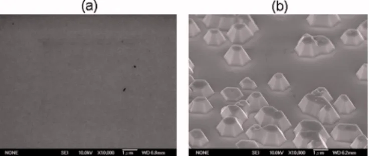
Figures 1共a兲 and 1共b兲 show the typical top-view scanning-electron microscopy 共SEM兲 images of samples grown without and with the growth-interruption step,
respec-tively. As shown in Fig. 1共a兲, the surface morphology of the LED I is near featureless. In contrast, the LED II exhibited a multitude of truncated micropyramids on the surface, as shown in Fig. 1共b兲. Following is the speculative description of the possible growth mechanism of the truncated micropy-ramids. During the growth-interruption step, only TMGa was switched off, and other growth conditions were retained. Such treatment may provide an inert surface for Mg atom adhesion caused by the filled dangling bonds on the surface of the initial p-GaN layer and thereby enhance the subse-quent growth of the truncated micropyramids. Thus the three-dimensional growth of subsequent p-GaN microcrys-tals on the Mg-treatment surface occurred predominantly be-fore the islands expanded laterally. As a result, a multitude of truncated micropyramids on the p-GaN layer could be achieved through the application of Mg-treatment process. In the growth of self-assembled microcrystal systems, most of the growth methods are related to the Stranski–Krastanov 共SK兲 mode.8,9
Unlike the SK mode, Mg-treatment approach does not require the formation of a wetting layer. In other words, the Mg dissolved from CP2Mg might be a surfactant that can be used to change the surface free energy of sub-strate共initial p-GaN layer兲. For example, As, Sb, or Sn, have been introduced onto the Si/ Ge substrate surface to suppress island formation by modifying surface free energies.10–12In this study, CP2Mg was introduced as a surfactant in order to enhance three-dimensional growth, which is contrary to the suppression occurring in the Ge/ Si system using some for-eign atoms. By introducing the CP2Mg precursor to the sub-strate surface共initial p-GaN layer兲, the surface free energy may be increased and thereby three-dimensional growth of subsequent p-GaN microcrystals can be enhanced. Addition-ally, the microcrystal size distribution can be controlled by annealing at different temperatures during the growth-interruption step or by increasing/decreasing subsequent growth time. However, the exact roles of CP2Mg are still unknown, and therefore a detailed study, including surface chemistry, needs to be carried out to clarify the formation mechanism.
For a conventional GaN-based LED, the vast majority of light emitted from an isotropic source incident on a GaN/air interface will undergo total internal reflection or Fresnel re-flection, passing a small amount of the light through the
GaN/air interface into air. It is a well-known fact that the
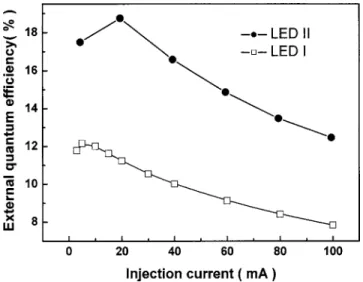
escape probability of photons emitting from a textured semi-conductor surface is higher than that of a smooth semicon-ductor surface.3 Figure 2 shows the typical EQE-current characteristics of LED I and LED II with a bare-chip form. With a 20 mA current injection, the typical output power of LED I and LED II was measured around 6 and 10 mW, respectively, when the LED chips were bonded on the TO 66 without resin encapsulation. It should be noted that all LEDs had an emission wavelength of around 465 nm when a dc current of 20 mA was applied. The EQE was around 11.25% and 18.75% for LED I and LED II, respectively, as shown in Fig 2. Thus, we can enhance the EQE by at least 60% by utilizing the Mg-treatment process. The enhancement of EQE in LED II can be attributed to the multitude of trun-cated micropyramids on the surface resulting in reduction of the reabsorption probability of the photons due to the fact that the photon path length is shorter before the photons escape into the free space.13,14 In other words, the escape cone of emitted photons in LED II would be larger than that FIG. 1. Top-view SEM micrographs of the InGaN/ GaN LEDs共a兲 without
and共b兲 with Mg-treatment process.
113505-2 Sheu et al. Appl. Phys. Lett. 88, 113505共2006兲
of LED I. The research assumptions can be indirectly sup-ported by the measurements of beam patterns of studied LEDs. As shown in Fig. 3, the typical beam patterns of LED I and LED II were determined at a dc driving current of 20 mA. It is clear that LED II displayed a narrower beam pattern. This is due to the fact that the photon path length is shorter in LED II before the photons escape into the free space. In other words, the most of generated photons were extracted from the top surface. In LED I, if photons are not absorbed by active layer after undergoing multiple reflec-tions betweenGaN/ sapphire and GaN/ air interfaces, they will be extracted from the periphery of LED. That is, the percentage of photons extracted from the periphery of LED I would be higher than that of LED II. As a result, the wider beam patterns were observed in LED I. However, it should be noted that photons undergoing multiple reflections in LEDs would result in the higher absorption probability by active layer and hence the reduction of EQE.
On the other hand, with a driving current of 20 mA, the forward voltages of LED I and LED II were 3.1 and 3.25 V, respectively. To understand the effect of surface morphology on device series resistance, dynamic resistances of the LEDs were also evaluated. For these two LEDs, experimental re-sults revealed that the series resistance was about 10 and 15⍀ for LED I and LED II, respectively. The slightly higher forward voltage of the LED II may be related to the forma-tion of the high-resistivity thin MgxNylayer between the
ini-tial p-GaN layer and the second p-GaN contact layer. It is an acknowledged fact that high series resistance in LED can cause a severe heating effect, giving rise to the carrier leak-age from the InGaN active region especially under high cur-rent operation. The heating effect will accelerate the degra-dation of electrodes and thereby influence the device reliability. According to the preliminary results of life tests, no significant difference between LED I and LED II could be observed. It should be noted that these LEDs were driven by a 20 mA injection current at room temperature during the burn-in tests. To further clarify whether the growth interrupt process will result in a significant degradation or not, burn-in tests performed at high temperature共80 °C兲 and high driving current共50 mA兲 are under way and results will be published elsewhere.
In summary, the research has demonstrated electrical and optical properties of GaN-based LEDs with the naturally tex-tured surface formed by application of a growth-interruption step and Mg-treatment processes. Experimental results indi-cated that GaN-based LED with trunindi-cated micropyramids on the surface exhibited a⬃60% enhancement in output power. The enhancement can be attributed to the reduction of the photon extraction path length made possible by rough LED surface. We should also note that the typical 20 mA driven forward voltage is only 0.15 V higher than that of conven-tional LEDs共without the Mg-treatment process兲.
The authors would like to thank the Center for Micro/ Nano Technology Research, National Cheng Kung Univer-sity, Tainan, Taiwan, for equipment access and technical sup-port and the National Science Council of Taiwan for financially supporting this research under Contract No. NSC94-2215-E-006-015.
1E. F. Schubert, Light Emitting Diodes共Cambridge University Press,
Cam-bridge, 2003兲, p. 185.
2R. J. Shul, L. Zhang, A. G. Baca, C. G. Willison, J. Han, S. J. Pearton, F.
Ren, J. C. Zolper, and L. F. Lester, Mater. Res. Soc. Symp. Proc. 573, 271 共1999兲.
3L. W. Wu, S. J. Chang, Y. K. Su, R. W. Chuang, Y. P. Hsu, C. H. Kuo, W.
C. Lai, T. C. Wen, J. M. Tsai, and J. K. Sheu, Solid-State Electron. 47, 2027共2003兲, and references therein.
4C. S. Chang, S. J. Chang, Y. K. Su, C. H. Kuo, W. C. Lai, Y. C. Lin, Y. P.
Hsu, S. C. Shei, J. M. Tsai, H. M. Lo, J. C. Ke, and J. K. Sheu, IEEE Trans. Electron Devices 50, 2208共2003兲.
5T. C. Wen, S. J. Chang, Y. K. Su, L. W. Wu, C. H. Kuo, W. C. Lai, J. K.
Sheu, and T. Y. Tsai, J. Electron. Mater. 32, 419共2003兲.
6J. K. Sheu, J. M. Tsai, S. C. Shei, W. C. Lai, T. C. Wen, C. H. Kou, Y. K.
Su, S. J. Chang, and G. C. Chi, IEEE Electron Device Lett. 22, 460 共2001兲.
7C.-W. Hu, A. Bell, F. A. Ponce, D. J. Smith, and I. S. T. Tsong, Appl.
Phys. Lett. 81, 3236共2002兲.
8C. Adelmann, N. Gogneau, E. Sarigiannidou, J. L. Rouvière, and B.
Daudin, Appl. Phys. Lett. 81, 3064共2002兲.
9M. Miyamura, K. Tachibana, and Y. Arakawa, Appl. Phys. Lett. 80, 3937
共2002兲.
10M. Copel, M. C. Reuter, E. Kaxiras, and R. M. Tromp, Phys. Rev. Lett.
63, 632共1989兲.
11D. J. Eaglesham, F. C. Unterwald, and D. C. Jacobson, Phys. Rev. Lett.
70, 966共1993兲.
12S. Iwanari and K. Takayanagi, Jpn. J. Appl. Phys., Part 2 30, L1978
共1991兲.
13R. Windisch, P. Heremans, A. Knobloch, P. Kiesel, G. H. Döhle, B. Dutta,
and G. Borghs, Appl. Phys. Lett. 74, 2256共1999兲.
14I. Schnitzer, E. Yablonovitch, C. Caneau, T. J. Gmitter, and A. Scherer,
Appl. Phys. Lett. 63, 2174共1993兲. FIG. 2. External quantum efficiency as a function of injection current
for InGaN/ GaN LEDs without 共LED I兲 and with Mg-treatment process 共LED II兲.
FIG. 3. Typical beam patterns taken from LED I and LED II. These LEDs were all bonded on the TO 66.
113505-3 Sheu et al. Appl. Phys. Lett. 88, 113505共2006兲