Chapter 3
Laser Direct-writing Optical Waveguides in Fused Quartz Glass
With the basic propagation theory of the optical waveguide and the fabrication that caused defects have been explained in Chapter 2. This Chapter, we will try to fabricate a waveguide device in a fused quartz glass by using the laser direct-writing technique. As a result of the excellent writing characteristics of a short-pulse laser micromachining result have been exhibited in fabricated waveguide devices; we focus our attentions on laser direct-writing waveguide by the source of Nd:YVO
4laser. The content of chapter 3 is arranged as followed: Section 3-1 is the introduction of laser-fabricated waveguide devices. In Section 3-2, the process of device fabrication has been discussed. The results for laser direct-writing waveguides are presented in Section 3-3. Finally, we also give the summary and discussion in section 3-4.
29
3-1 Introduction of Laser-Fabricated Waveguide Devices
As the technique of planar light-wave circuits in an advanced optical waveguide is developing, there is an increasing demand in simplified PLC production methods that improve of reliability to the component manufacture and reduce the cost. One such technique is laser-fabricated, originally demonstrated in the 1980’s [50-52]. Lasers can also work on most materials and are environmentally friendly [67]. The energy deposition is based on multi-photon absorption and avalanche ionization;
the nonlinearity of the process can be exploited in order to write structures into the bulk of materials. Another advantage of this fabrication process is the capability of rapid prototyping of a device without the need for any photolithographic process. Recent publications have proposed the possibility of percussion drill and refractive index change by infrared ultra-fast lasers exposure of glasses in their transparent spectral region.
Most of them have reported this effect in silica [54], PMMA [55-56], or Porous Silicon [57]. Laser-fabricated waveguide have become a promising fabrication route for optical waveguides materials, allowing reliable, cost-effective and without resorting to the complexity of conventional fabrication techniques.
30
3-1-1 Laser Direct-writing of Buried Waveguides in Glass
Since the first evidence to the possibility of writing channel waveguides by infrared short pulses. Photo induced refractive index change in oxide glasses has been widely used to fabricate different optical elements such as channel waveguides and gratings by means of direct laser writing.
Infrared lasers are attractive for direct-writing of 3-D photonic structures [58] such as those required in an integrated-optical circuit application.
Direct-writing technique has the advantage of allowing rapid and inexpensive prototyping, in contrast to conventional mask-based photolithographic approaches in which a mask must be designed and fabricated before waveguides can be produced. This process also has the advantage of direct-writing features within restricted regions of a sample without the surrounding area. The fabrication of local structures generally involves a multi-step process which affects the entire surface as opposed to conventional techniques. The basic physical mechanisms underlying refractive index modification can be described as followed [59]. The high intensities in the focal volume give rise to nonlinear absorption mechanisms such as multi-photon and avalanche ionization, which create
31
hot electron plasma in a small volume around the focal point. Energy is then rapidly transferred to the lattice, resulting in a large increase of both temperature and pressure. These are induced, by mechanisms not yet completely understood, a local variation of the refractive index which, under suitable circumstances, can be positive. By translating the sample with respect to the laser focus, one can create three-dimensional guiding structures inside the bulk of the material. The material modification is strongly dependent on glass composition, pulse wavelength, energy, and repetition rate, as well as on sample translation speed. For this reason, direct-writing technique affords considerable latitude in focusing, power level, and scanning speed. Then we will permit the creation of novel structures that are virtually impossible to fabricate by mask lithography, such as waveguides with a varying refractive index along the direction of propagation. This advantage also makes possible the patterning of substrates that contain elevated structures that prevent mask contact printing.
This technique presents advantages compared to other complicated fabrication processes including lithography and dry etching since besides being a one step process, is not limited to photosensitive glasses. This
32
new situation has made it necessary to deeply explore and properly characterize the devices made using this new fabrication technology.
Recently, direct-writing waveguide and have been accomplished by generating line damage inside various glasses. A large number of photonic devices have been successfully fabricated using this technique, including channel waveguides and Y-couplers, rare earth-doped waveguide amplifiers, holograpic gratings, birefringent structures, directional couplers tubular waveguides, and active waveguides [60-67].
33
3-2 Direct-writing Device Fabrication Process
Laser micromachining as the material processing technology requires finding numerous real world applications. In this paper, we present results of forming visible and infrared transmitting buried waveguides in fused quartz glass with used laser of diode-pumped solid-state (DPSS) Neodymium-doped yttrium orthovanadate (Nd:YVO
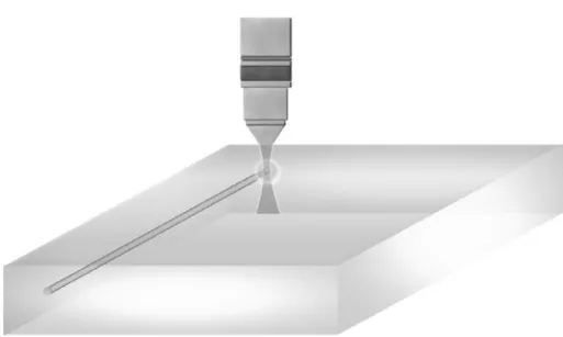
4). We fabricated waveguide in silica by direct-writing technique with a refractive index change. The experimental setup for waveguide writing is very simple and is depicted schematically in Fig. 3.1. Without complicated step, we have an easy way to writing waveguide in one step process. This has the advantage of this; fabrication just needs design our waveguide devices and wait a few minutes to get the results.
In this experiment, we used two types of lasers, the long pulse (Nd:YAG) and short pulse (Nd:YVO
4) laser. We also use two kinds of material with two write technologies to fabricate our waveguide. Here laser writing in fused quartz glass will be fabricated and discussed, and we will study laser writing waveguide based on SOI wafer in the next Chapter.
34
3-2-1 Neodymium-Doped Yttrium Orthovanadate (Nd:YVO
4) Laser
Laser micromachining as the material processing technology on small and very small scale is finding numerous real world applications. [69]
Nd:YVO
4is becoming a very important solid state laser material. A larger absorption coefficient, broader absorption bandwidth and larger stimulated emission cross-section at the lasing wavelength of doped Nd:YVO
4crystals are three major advantages of Nd:YVO
4crystals over other materials in the design of diode-pumped solid state lasers.
Neodymium doped Yttrium Orthovanadate, Nd:YVO
4, is often simply referred to as “vanadate". Vanadate crystals are an ideal host for trivalent Nd ions, and are emerging as one of the most popular choices for gain elements used in diode pumped solid state lasers. Together with the newest technologies diode-pumped solid-state (DPSS) lasers are moving from research laboratories to production lines.
Vanadate’s broad absorption peak means that it can be pumped at high efficiency over a wide wavelength range. As a result, the laser output power is less affected by wavelength drifts of the pump diode. These
35
drifts might be caused by temperature changes or ageing effects. The crystals short fluorescence lifetime is an advantage for high-repetition rate Q-switched operation [68].
In this chapter, we used a Pico-second high power and high pulse energy diode-pumped solid-state (DPSS) laser [69]. Which compact laser with 10 W output power at 1064 nm. It features high pulse energy (up to 200 µJ), high beam quality (M² < 1.5) and a very high repetition rate (up to 100 kHz) of typically 10 ps pulses. Optional harmonics are available at wavelength 532 nm, 355 nm and 266 nm.
3-2-2 Setup for Waveguide Writing
As shown in Fig. 3.1, we write the channel waveguide in fused quartz glass by a laser change refractive index. Energy is then rapidly transferred to the lattice, resulting in a large increase of both temperature and pressure by the high intensities in the focal volume give rise to nonlinear absorption mechanisms [70]. Such as multi-photons and avalanche ionization, those create hot electron plasma in a small volume around the focus. A local variation of the refractive index can be an experimentation.
36
For the experimental setup for waveguide writing is a one step process and just needs few minutes to get the results. There will be many chances to try various factors and analysis of the results. Here the average power of Nd:YVO
4laser we used is from 10W (100%) ~ 2W (20%), which means 20% ~100% of energy 0.1 mJ @ 100 kHz. The laser writing speed was 5, 25 and 50 mm/s with a shoot density of 1000 Pulses/mm. In this experiment, we will try to write from a power of 2W to 10W with increase of 1W. Besides, we use three speeds to test the writing effects.
The material which we used is fused quartz glass of thickness 0.5 mm.
From different kinds of power and writing speed, we will get a better way to fabrication optical waveguide which we can apply in the future.
37
3-3 Results of Direct-writing Channel Waveguide in Fused Quartz Glass
This section we will have three parts to discuss the result of our waveguides. First, we will discuss the fused quartz glass which was demonstrated by the top view of pictures. The speeds of 25 mm/s and 50 mm/s will be discussed in section 3-3-2 respectively.
3-3-1 Analysis of Waveguides with Writing Speed of 5 mm/s
In this section, we use Nd:YVO
4laser with an average power from 10W to 2W. The laser writing speed was 5 mm/s with a shoot density of 1000 Pulses/mm. As Fig. 3.2 shows, we have tested nineteen waveguides with different writing powers and depths. Because the thickness of the fused quartz glass is 0.5 mm, it is not easy to write accurately in a fused quartz glass. We have tried various factors for the analysis of the results.
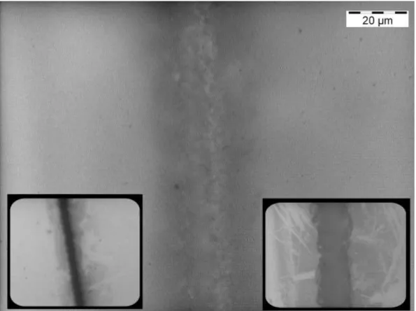
From Fig. 3.3 and Fig. 3.4, we have first tested the writing depth with an average power 10W and 9W. Different results are also observed when the average power is changed: waveguide roughness which have been written with an average power of 9W looks more serious than the Waveguide which wrote at a power of 10W. The widths of the two waveguides are
38
about 20μm.
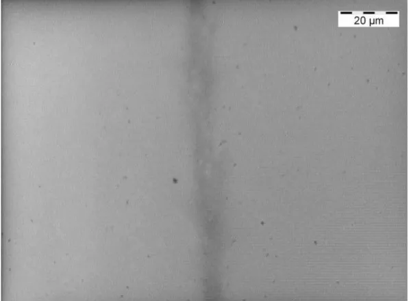
Then we change the writing depth. From Fig. 3.3 and Fig. 3.5, those two waveguides have the same writing speeds and the same writing power of 10W. But different writing depths lead different waveguide widths. It can also be observed that the waveguide in Fig. 3.5 looks smoother than the Waveguide in Fig. 3.3.
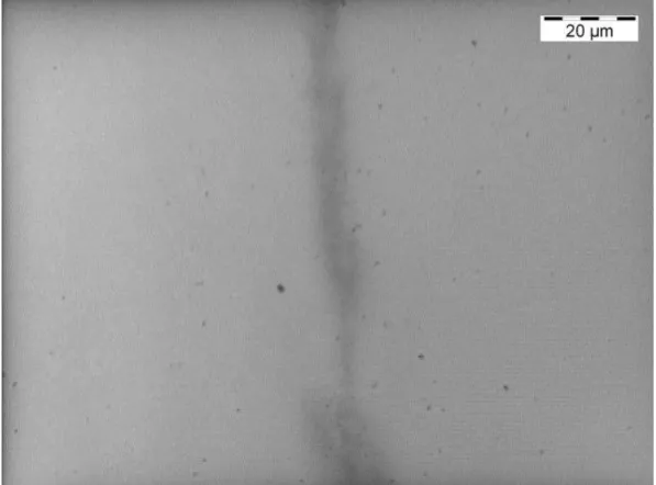
In Fig. 3.5, Fig. 3.6 and Fig. 3.7, we can magnify the waveguide by microscope with different object lens and different focal distance. The waveguide which is writing at 10W looks smoother than other two waveguides. From Fig. 3.8 to Fig. 3.12, with writing at power of 6W to 2W, the waveguides were forks and intermittently.
3-3-2 Analysis of Waveguides with Writing Speed of 25 mm/s and 50 mm/s
In this section, we also use Nd:YVO
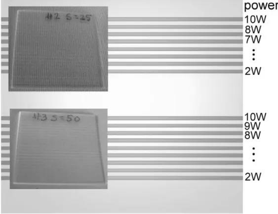
4laser with average power from 10W (100%) ~ 2W (20%). The laser writing speed was 25 mm/s with a shoot density of 1000 Pulses/mm. Fig. 3.13 shows the top view of this fused quartz glass. We have tested seventeen waveguides with different writing powers and depths in fused quartz glass which has a thickness of 0.5 mm.
39
In Fig. 3.14, Fig. 3.15 and Fig. 3.16, from different object lens and different focal distance, we can see the waveguide with writing at 10W which looks smoother than other two Waveguides. From Fig. 3.17 to Fig.
3.21, the waveguides were also forks and intermittent when writing at a power of 6W to 2W.
We changed the writing speed to 50 mm/s. It is not easy to discriminate between writing at 10W and 8W from Fig. 3.22 and Fig. 3.23. Both of them have arc sidewall’s roughness clearly. From Fig. 3.24 to Fig. 3.29, the waveguides are very similar when writing at a power of 7W to 2W.
From all the pictures mentioned above, we can say that with a high power and low speed, direct-writing channel waveguide will be better and smoother.
40
3-4 Discussion and S ummary
Laser direct-writing technique was originally demonstrated in the 1980’s, and can also work on most materials and is environmentally friendly. The energy deposition is based on multi-photon absorption and avalanche ionization; the nonlinearity of the process can be exploited in order to write structures into the bulk of materials.
In this Chapter, we have demonstrated the possibility of writing optical waveguides by means of a Pico-second high power and high pulse energy diode-pumped solid-state (DPSS) laser. An analysis of the characteristics of the waveguides written with different pulse energies, depths, and translation speeds is presented, and an optimum set of writing parameters is evidenced. With a written power of 10W and at speed of 5 mm/s, optical buried waveguides will look smoother. Lower power or higher speed will cause the waveguide roughness to be obvious.
Future work will concentrate on investigating the dependence of the waveguide characteristics on fabrication parameters, such as refractive index change and transmittance. A systematic study will lead to buried waveguides with controlled modal characteristics for the implementation
41
of an integrated waveguide laser or a two-dimensional array of active waveguides.
42
Fig. 3.1 Direct-writing the channel waveguide in fused quartz glass.
Fig. 3.2 Top view of the channel waveguides which fabricated by the speed of 5mm/s.
43
Fig. 3.3 The OM picture of channel waveguide in fused quartz glass with writing speed of 5mm/s and power of 10 W.
Fig. 3.4 The OM picture of channel waveguide in fused quartz glass with writing speed of 5mm/s and power of 9 W.
44
Fig. 3.5 The OM picture of channel waveguide in fused quartz glass with writing speed of 5mm/s and power of 10 W.
Fig. 3.6 The OM picture of channel waveguide in fused quartz glass with writing speed of 5mm/s and power of 8 W.
45
Fig. 3.7 The OM picture of channel waveguide in fused quartz glass with writing speed of 5mm/s and power of 7 W.
Fig. 3.8 The OM picture of channel waveguide in fused quartz glass with writing speed of 5mm/s and power of 6 W.
46
Fig. 3.9 The OM picture of channel waveguide in fused quartz glass with writing speed of 5mm/s and power of 5 W.
Fig. 3.10 The OM picture of channel waveguide in fused quartz glass with writing speed of 5mm/s and power of 4 W.
47
Fig. 3.11 The OM picture of channel waveguide in fused quartz glass with writing speed of 5mm/s and power of 3 W.
Fig. 3.12 The OM picture of channel waveguide in fused quartz glass with writing speed of 5mm/s and power of 2 W.
48
Fig. 3.13 Top view of the channel waveguides which was fabricated by the speed of 25mm/s and 5mm/s.
Fig. 3.14 The OM picture of channel waveguide in fused quartz glass with writing speed of 25mm/s and power of 10 W.
49
Fig. 3.15 The OM picture of channel waveguide in fused quartz glass with a writing speed of 25mm/s and power of 8 W.
Fig. 3.16 The OM picture of channel waveguide in fused quartz glass with a writing speed of 25mm/s and power of 7W.
50
Fig. 3.17 The OM picture of channel waveguide in fused quartz glass with writing speed of 25mm/s and power of 6 W.
Fig. 3.18 The OM picture of channel waveguide in fused quartz glass with a writing speed of 25mm/s and power of 5 W.
51
Fig. 3.19 The OM picture of channel waveguide in fused quartz glass with a writing speed of 25mm/s and power of 4 W.
Fig. 3.20 The OM picture of channel waveguide in fused quartz glass with a writing speed of 25mm/s and power of 3 W.
52
Fig. 3.21 The OM picture of channel waveguide in fused quartz glass with a writing speed of 25mm/s and power of 2 W.
Fig. 3.22 The OM picture of channel waveguide in fused quartz glass with a writing speed of 50mm/s and power of 10 W.
53
Fig. 3.23 The OM picture of channel waveguide in fused quartz glass with a writing speed of 50mm/s and power of 8 W.
Fig. 3.24 The OM picture of channel waveguide in fused quartz glass with a writing speed of 50mm/s and power of 7 W.
54
Fig. 3.25 The OM picture of channel waveguide in fused quartz glass with a writing speed of 50mm/s and power of 6 W.
Fig. 3.26 The OM picture of channel waveguide in fused quartz glass with a writing speed of 50mm/s and power of 5 W.
55
Fig. 3.27 The OM picture of channel waveguide in fused quartz glass with a writing speed of 50mm/s and power of 4 W.
Fig. 3.28 The OM picture of channel waveguide in fused quartz glass with a writing speed of 50mm/s and power of 3 W.
56
Fig. 3.29 The OM picture of channel waveguide in fused quartz glass with a writing speed of 50mm/s and power of 2 W.
57