Near-infrared femtosecond laser-induced crystallization of amorphous silicon
Jia-Min Shieh, Zun-Hao Chen, Bau-Tong Dai, Yi-Chao Wang, Alexei Zaitsev, and Ci-Ling Pan
Citation: Applied Physics Letters 85, 1232 (2004); doi: 10.1063/1.1782267 View online: http://dx.doi.org/10.1063/1.1782267
View Table of Contents: http://scitation.aip.org/content/aip/journal/apl/85/7?ver=pdfcov
Published by the AIP Publishing
Articles you may be interested in
Crystallization kinetics of ultrathin amorphous Si film induced by Al metal layer under thermal annealing and pulsed laser irradiation
J. Appl. Phys. 101, 043518 (2007); 10.1063/1.2654512
Kinetics of laser-induced low-temperature crystallization of amorphous silicon
Appl. Phys. Lett. 81, 3347 (2002); 10.1063/1.1516875
Excimer laser annealing of amorphous and solid-phase-crystallized silicon films
J. Appl. Phys. 86, 5556 (1999); 10.1063/1.371560
Laser crystallization and structural characterization of hydrogenated amorphous silicon thin films
J. Appl. Phys. 85, 7914 (1999); 10.1063/1.370607
Short-pulse laser-induced crystallization of intrinsic and hydrogenated amorphous germanium thin films
J. Appl. Phys. 82, 5159 (1997); 10.1063/1.366320
This article is copyrighted as indicated in the article. Reuse of AIP content is subject to the terms at: http://scitation.aip.org/termsconditions. Downloaded to IP: 140.113.38.11 On: Thu, 01 May 2014 04:15:06
Near-infrared femtosecond laser-induced crystallization
of amorphous silicon
Jia-Min Shieh, Zun-Hao Chen, and Bau-Tong Dai
National Nano Device Laboratories, Hsinchu 300, Taiwan, Republic of China Yi-Chao Wang, Alexei Zaitsev, and Ci-Ling Pana)
Institute of Electro-Optical Engineering, National Chiao Tung University, Hsinchu 30050, Taiwan, Republic of China
(Received 6 October 2003; accepted 15 June 2004)
Amorphous silicon 共a-Si兲 was crystallized by femtosecond laser annealing (FLA) using a near-infrared 共⬇800 nm兲 ultrafast Ti:sapphire laser system. The intense ultrashort laser pulses lead to efficient nonlinear photoenergy absorption and the generation of very dense photoexcited plasma in irradiated materials, enabling nonlinear melting on transparent silicon materials. We studied the structural characteristics of recrystallized films and found that FLA assisted by spatial scanning of laser strip spot constitutes superlateral epitaxy that can crystallize a-Si films with largest grains of⬃800 nm, requiring laser fluence as low as ⬃45 mJ/cm2, and low laser shots. Moreover,
the optimal annealing conditions are observed with a significant laser-fluence window共⬃30%兲. ©
2004 American Institute of Physics. [DOI: 10.1063/1.1782267]
High-performance silicon devices on insulators have re-cently been incorporated in various applications, such as ac-tive matrix liquid crystal displays(AMLCD) and lightweight flat panel displays. The key component for realizing such systems is low-temperature polycrystalline silicon (LTPS) thin-film transistors(TFTs). Low-thermal-budget techniques, such as plasma-assisted hydrogen-,1 metal-,2 and laser-induced crystallization3–10are commonly employed to crys-tallize the channel regions of LTPS-TFTs. In particular, effi-cient absorption of ultraviolet (UV) laser irradiation by amorphous silicon共a-Si兲 results in high-quality polycrystal-line silicon(pc-Si) by excimer laser annealing (ELA).3–7The introduction of the sequential lateral solidification (SLS) technique,6,8,9based on a controlled superlateral growth (C-SLG) method,6–9can form single-crystalline silicon in active regions of processed devices.6–9
Unlike annealing using continuous-wave(cw)10and long pulse lasers, nonlinear photoenergy absorption and nonequi-librium thermodynamics are expected to dominate the inter-actions between the intense femtosecond laser pulses and irradiated transparent materials.11–16 Such a nonlinear pro-cess provides precise and low-threshold fluence associated with femtosecond laser ablation.13–16 In this letter we study the structural characteristics of recrystallized amorphous sili-con films. We report infrared femtosesili-cond laser-induced crystallization of amorphous silicon with high crystallinity, using ultralow laser energy.
Silane-based a-Si films共100 nm兲 were deposited on oxi-dized共500 nm兲 silicon wafers by low-pressure chemical va-por deposition(LPCVD) at 550 °C. An infrared femtosec-ond Ti:sapphire laser system14 (TSUNAMI, and SPIT FIRE, from the Spectra-Physics Company) with a wavelength of 800 nm, a repetition rate of 1 kHz, a pulse duration in the range of 50– 125 fs, and an output energy per pulse of ⬃0.5 mJ, was guided to crystallize amorphous silicon. All samples were placed in a vacuum chamber, and a heater
increased the substrate temperature up to 400 ° C. First, we made a steady-state multiple shot femtosecond laser anneal-ing (FLA) experiment. The pulse train from the aforemen-tioned laser system was focused in the strip spot 共3 mm ⫻250m兲. We changed the fluence 共38–63 mJ/cm2兲 and the number of shots(5–100). Scanning electron microscopy (SEM) pictures of annealed areas (Fig. 1) with obvious grain boundaries, obtained by delineating defects using Secco etching, show the high uniformity of poly-Si grains. Pictures (a)–(d) in Fig. 1 represent steady-state multishot samples ir-radiated with 20 laser pulses of 50 fs with different energy densities. The average grain size is relatively small (lower than 50 nm) and almost independent on the energy density (see Fig. 1). It should be mentioned that in comparison to linear ELA for nonlinear steady-state FLA, small grains 共⬍50 nm兲 might be due to the fact that fast cooling (or laser-energy turn off) associated with short pulses causes random recrystallization from more nucleation sites.7
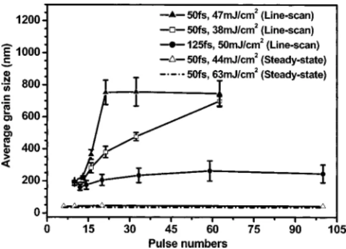
The situation is dramatically changed if we introduce scanning. In our second experiment we scan the laser beam along the sample with the speed of 2.5– 25 mm/ s (10–100 laser shots per unit area, or, equivalently, an overlapping of 90%–99%). Pictures (e)–(h) in Fig. 1 represent line-scan FLA samples irradiated with a 95% interpulse overlapping of 50 fs laser pulses with different energy densities. As shown in Fig. 2, the average grain sizes of FLA pc-Si films are plotted as a function of laser-energy density(denoted as EL) and pulse duration for both steady-state and line-scan FLA. Herein, annealing parameters for line-scan (steady-state) FLA were overlapping⬃95% (20 laser shots). For line-scan FLA using 125 fs pulses, the grain sizes of the crystallized
a-Si films initially increases, and then saturates, before
fi-nally declining as the laser fluence was increased from 35 to 61 mJ/ cm2. The maximum average grain size was
around 200 nm when a-Si films were irradiated at 50 mJ/ cm2. Despite the difference between the mechanism of photoexcitation melting using FLA (nonlinear annealing)11–15 and that when using nanosecond or longer pulse laser annealing(linear annealing), such as ELA, lateral a)Electronic mail: [email protected]
APPLIED PHYSICS LETTERS VOLUME 85, NUMBER 7 16 AUGUST 2004
0003-6951/2004/85(7)/1232/3/$20.00 1232 © 2004 American Institute of Physics
This article is copyrighted as indicated in the article. Reuse of AIP content is subject to the terms at: http://scitation.aip.org/termsconditions. Downloaded to IP: 140.113.38.11 On: Thu, 01 May 2014 04:15:06
elongating still dominates the growth of grains in FLA pc-Si films. The SLG phenomena,5–7thus predicts the trend plotted in Fig. 2. For line-scan FLA using short pulses with 50 fs duration, the trend in average grain sizes of FLA pc-Si films versus ELis similar to that obtained with 125 fs pulses, but
the maximum average grain size 共800 nm兲 of crystallized films, and the optimal ELof crystallization 共47 mJ/cm2兲 for
FLA using 50 fs pulses are markedly better than those for FLA using 125 fs pulses. The increase in the efficiency of nonlinear photoenergy absorption15,16with the peak power of the laser pulses during infrared FLA, is responsible for the dependence of the grain sizes of line-scan FLA pc-Si films on the duration of pulses, and the laser fluence.
It is remarkable that the maximum of average grain size 共⬃800 nm兲 equals the wavelength used. This phenomenon is also observed in ELA,17 in multiple pulse irradiation. Typi-cally, this is related to interference effects at the surface due to the reflection of the hillocks that are formed at the grain boundaries. But in FLA we do not observe such a kind of phenomena in steady-state multiple shot experiments. Only scanning leads to grain elongating.
The examination of grain sizes of line-scan FLA pc-Si films crystallized at various overlapping interpulses, at EL values of 47 and 38 mJ/ cm2for 50 fs pulses, and 50 mJ/ cm2 for 125 fs pulses, is indicated in Fig. 3. The required laser shots are lower for FLA using shorter pulses and higher EL.
But again we should mention that increasing the pulse
num-bers or shots in steady-state FLA does not result in the en-largement of crystallized grains(Fig. 3). On the other hand, the data in Figs. 2 and 3 for line-scan FLA clearly demon-strates the high effectiveness of scanning and nonlinear pho-toabsorption in crystallizing amorphous silicon. Assuming a Gaussian shape of the laser beam, for the steady-state mode, each illuminated point is repeatedly shined by the same en-ergy. First, a few laser pulses transform amorphous material into a polyphase with large grain distribution. Last, pulses (with the same energy) cannot significantly change that dis-tribution. In line-scan mode, each illuminated point is also repeatedly shined. But the shined energy for the considered area is not the same from pulse to pulse. It follows Gaussian law. That is a possible reason for why smaller grains have possibilities in gaining larger energy, therefore, resulting in grain regrowing into larger grains. Thus, the suggested SLS-like mechanism, assisted with the feature of low melting en-ergy for small grains obtained with steady-state FLA, signifi-cantly enlarge the grain size of line-scan FLA pc-Si films. Moreover, for ultrashort laser pulses, the melting thickness is determined by nonlinear absorption skin depth rather than heat penetration length due to thermal conduction,15and thus more insensitive to laser fluence in comparison with that for linear annealing. Besides the proposed SLS-like mechanism, this melting-depth thinning mechanism during FLA is also responsible for the significant process window in laser flu-ence共45–60 mJ/cm2兲 for line-scan FLA using 50 fs pulses. FIG. 1. SEM pictures of FLA pc-Si samples after Secco etching for steady-state(a), (b), (c), (d) and scanned FLA (e), (f), (g), (h).
FIG. 2. Average grain sizes of FLA pc-Si films, irradiated with pulses of different durations, as a function of laser fluence for steady-state FLA and scanned FLA.
FIG. 3. Average grain sizes of FLA pc-Si films, irradiated with pulses of different durations, as a function of interpulse overlapping for steady-state FLA and scanned FLA.
Appl. Phys. Lett., Vol. 85, No. 7, 16 August 2004 Shiehet al. 1233
This article is copyrighted as indicated in the article. Reuse of AIP content is subject to the terms at: http://scitation.aip.org/termsconditions. Downloaded to IP: 140.113.38.11 On: Thu, 01 May 2014 04:15:06
The rms roughness measured by atomic force micros-copy (AFM) of all FLA pc-Si films is below 4.5 nm. The peak-to-peak roughness is about 26 nm for line-scan FLA samples. Figures 4(a) and 4(b) represent the AFM images of line-scan and steady-state FLA pc-Si films, respectively.
The characteristics and annealing parameters for silicon films crystallized by FLA herein are compared with those obtained by other annealing methods3,5,10,18and summarized in Table I. The intense ultrashort laser pulses lead to efficient nonlinear photoenergy adsorption in irradiated materials, en-abling a melting of a-Si films. FLA assisted by a spatial scanning of the laser strip spot efficiently crystallizes a-Si films with large average grains of 800 nm, using a total laser energy as low as⬃0.9 J/cm2. Moreover, FLA exhibits a sig-nificant operating window for laser fluence (⬃30% varia-tions), which makes it possible to implement the suggested method in the TFT industry.
The authors would like to thank the support of the Na-tional Science Council, through Contract Nos. 492-007, 492-012, and NSC92-2215-E-492-011, and the Program for Pursuit of Academic Excellence of the Ministry of Education, Republic of China.
1
S. Sriraman, S. Agarwal, E. S. Aydil, and D. Maroudas, Nature(London)
418, 62(2002).
2
G. A. Bhat, Z. Jin, H. S. Kwok, and M. Wong, IEEE Electron Device Lett.
20, 97(1999).
3
J. S. Im, H. J. Kim, and M. O. Thompson, Appl. Phys. Lett. 63, 1969 (1993).
4
G. K. Giust and T. W. Sigmon, Appl. Phys. Lett. 70, 767(1997).
5
S. D. Brotherton, D. J. McCulloch, J. P. Gowers, J. R. Ayres, and M. J. Trainor, J. Appl. Phys. 82, 4086(1997).
6
J. S. Im, M.A. Crowder, R. S. Sposili, J. P. Leonard, H. J. Kim, J. H. Yoon, V. V. Gupta, H. J. Song, and H. S. Cho, Phys. Status Solidi A 166, 603 (1998).
7
A. T. Voutsas, Appl. Surf. Sci. 208, 250(2003).
8
M. A. Crowder, P. G. Carey, P. M. Smith, R. S. Sposili, H. S. Cho, and J. S. Im, IEEE Electron Device Lett. 19, 306(1998).
9
R. Dassow, J. R. Köhler, Melanie Nerding, M. Grouvogl, R. B. Bergmann, and J. H. Werner, Solid State Phenom. 67–68, 193(1999).
10
A. Hara, F. Takeuchi, and N. Sasaki, IEEE Electron Devices Society, Proc. of 2000 International Electron Device Meeting(2000), p. 209.
11
S. K. Sundaram and E. Mazur, Nat. Mater. 1, 217(2002).
12
A. Rousse, C. Rischel, S. Fourmaux, I. Uschmann, S. Sebban, G. Grillon, Ph. Balcou, E. Förster, J. P. Geindre, P. Audebert, J. C. Gauthier, and D. Hulin, Nature(London) 410, 65 (2001).
13
K. Sokolowski-Tinten, J. Biakowski, and D. von der Linde, Phys. Rev. B
51, 14186(1995).
14
T. Y. Choi and C. P. Grigoropoulos, J. Appl. Phys. 92, 4918(2002).
15
X. Liu, D. Du, and G. Mourou, IEEE J. Quantum Electron. 33, 1706 (1997).
16
T. Q. Jia, Z. Z. Xu, X. X. Li, R. X. Li, B. Shuai, and F. L. Zhao, Appl. Phys. Lett. 82, 4382(2003).
17
S. Horita, Y. Nakata, and A. Shimoyama, Appl. Phys. Lett. 78, 2250 (2001).
18
J. S. Im, R. S. Sposili, and M. A. Crowder, Appl. Phys. Lett. 70, 3434 (1997).
TABLE I. Comparison of characteristics and performances for silicon films crystallized by FLA herein with those obtained by other annealing methods.
FLA Single shot ELA(Ref. 3) Multishot ELA(Ref. 5) SLS ELA (Ref. 18) Green cw laser annealing (Ref. 10)
Crystallization mode SLS-like SLG SLG SLS
cw-lateral crystallization Optimal EL共mJ/cm2兲 ⬃45 150–250 150–450 ⬃900 Maximum of average grain sizes共m兲 ⬃0.8 ⬃1 ⬃0.3 ⬃200 ⬃20⫻3 Laser shots ⬎20 1 10–100 ⬃70
Total input energy
共J/cm2兲 ⬃0.9 ⬎0.15 ⬃10 ⬃60 ⬎10
FIG. 4.(a), (b) AFM images of FLA pc-Si films irradi-ated with 50 fs pulses. Line-scan(steady-state) mode is performed using ELof 46 mJ/ cm2共60 mJ/cm2兲 and an interpulse overlapping of 95%(20 laser shots).
1234 Appl. Phys. Lett., Vol. 85, No. 7, 16 August 2004 Shiehet al.
This article is copyrighted as indicated in the article. Reuse of AIP content is subject to the terms at: http://scitation.aip.org/termsconditions. Downloaded to IP: 140.113.38.11 On: Thu, 01 May 2014 04:15:06