國立交通大學
光電工程研究所
博士論文
具混合式反射鏡共振腔氮化鎵面
射型雷射之研究
Study of Nitride-Based Vertical-Cavity
Surface Emitting Lasers with Hybrid
Mirrors
研 究 生:高 志 強
指導教授:王 興 宗 教授
郭 浩 中 教授
國 立 交 通 大 學
光電工程研究所
博士論文
具混合式反射鏡共振腔氮化鎵面射型
雷射之研究
Study of Nitride-Based Vertical-Cavity
Surface Emitting Lasers with Hybrid
Mirrors
中華民國 九十六 年 九 月
研 究 生:高 志 強
指導教授:王 興 宗
郭 浩 中
Student: Chih-Chaing Kao
Advisor: Shing Chung Wang
具混合式反射鏡共振腔氮化鎵面射型雷
射之研究
Study of Nitride-Based Vertical-Cavity Surface
Emitting Lasers with Hybrid Mirrors
國立交通大學
光電工程研究所
博士論文
A dissertation
Submitted to Institute of Electro-optical Engineering
College of Electrical Engineering and Computer Science
National Chiao Tung University
In Partial Fulfillment of the Requirements
For the Degree of
Doctor of Philosophy
In Electro-Optical Engineering
September 2007
Hsin-chu, Taiwan, Republic of China
中華民國 九十六 年 九 月
研 究 生:高 志 強
指導教授:王 興 宗
郭 浩 中
Student: Chih-Chaing Kao
Advisor: Shing-Chung Wang
I
具混合式反射鏡共振腔氮化鎵面射型雷射之研究
研究生:高志強 指導教授:王興宗 教授
郭浩中 教授
國立交通大學光電工程研究所
摘要
在過去數年來,氮化鎵系列材料已被廣泛使用於許多光電元件諸如發光二極 體與雷射二極體以及光偵測器,而這些元件更被加以大量應用於光儲存、平面顯 示、照明及生物科技中。也因為其應用面相當的廣大,氮化鎵材料吸引了不少研 究的目光。 本論文旨在發展具混合式反射鏡共振腔之氮化鎵光激發面射型雷射的製作方 法並研究其雷射特性。在此研究中,所設計製作的氮化鎵面射型雷射乃由一個光 程約五倍波長的共振腔、一組鋁化鎵/氮化鎵之布拉格反射鏡與一組氧化物反射 鏡所組成。其雷射之臨界激發能量約為 2.6 mJ/cm2 而其所輻射波長為 456.2 nm 且 半高寬僅僅 0.2 nm.此外,其極化程度與發散角皆相當優異,可分別達到 84%與 7.6 度。更特別的是,此雷射的自發輻射耦合率高達 0.02,是一般邊射型雷射的 1000 倍之高,這代表著其效率被微共振腔大幅提高。我們還發現了多個雷射點與 穩定模態情況,這情況與共振腔與增益介質之不均勻有著極大關係。 我們進一步建立了電激發面射型雷射的製程並將此製程應用於光激發面射型 雷射結構上製作出一個具有非長高品質因子的微共振腔發光二極體。我們在製程 中使用了高透明度的氧化錫銦做為透明電極來減少吸收。此元件之發光波長落於 463.2 nm,於 10 微安時,其半高可達至 0.52 nm,即數值約 895 的品質因子。這 表示著已相當接近雷射操作的可能。 最後,我們更發展了光激發的光子晶體面射型雷射,我們製作了不同週期 (190 nm - 300 nm)的光子晶體且皆達到了大面積雷射操作,雷射波長落於 395 nm 到 425 nm。此種雷射具有的極化與發散角分別約為 53%與小於 10 度。由對照粗略理論的計算,我們發現雷射乃發生於光子晶體能帶的邊緣交集處,也就是滿足 布拉格條件處,且越大的光子晶體週期會對應到具較高的歸一頻率的能帶邊緣, 這可充份提供設計此種雷射的線索,而此實驗成果亦充份顯示此種雷射有相當大 潛力應用於高功率大面積單模雷射。
III
Study of Nitride-Based Vertical-Cavity Surface Emitting
Lasers with Hybrid Mirrors
Student: Chih-Chiang Kao Advisor: Dr. Shing-Chung Wang
Dr. Hao-Chung Kuo
Department of photonics & Institute of Electro-Optical Engineering National Chiao-Tung University
Abstrate
Over past few years, ntride-based materials have been widely used in several optoelectronic devices, such as light emitting diodes, laser diodes, and photo-detectors. These devices have highly potential in the applications such as flat panel display, competing storage technologies, automobiles, general lighting, and biotechnology, and so on. Therefore, nitride wide-bandgap devices have attracted lots of attention.
In this study, we have demonstrated the fabrication of the optically-pumped nitride-based vertical cavity surface emitting laser (VCSEL) with hybrid mirrors and investigated characteristics of this kind of laser. The nitride-based VCSEL was formed by a five-lamda (λ) micro-cavity sandwiched by hybrid DBR mirrors, consisting of AlN/GaN DBR and
Ta2O5/SiO2 DBR. The laser action was observed under the optical pumping at room
temperature with a threshold pumping energy density of about 2.6 mJ/cm2. The GaN VCSEL
emits 456 nm blue wavelength with a linewidth of 0.2 nm and the laser beam shows a large degree of polarization of about 84%, a high characteristic temperature to be about 244 K, and a small divergence angle to be about 7.6o. The coupling efficiency of spontaneous emission (β) of our VCSEL was fitted to be a value as high as 0.02, which is three order of magnitude
higher than that of the typical edge emitting semiconductor lasers (normally about 10-5), indicating the enhancement of the spontaneous emission into a lasing mode by the high quality factor microcavity effect in the VCSEL structure. Furthermore, we found the multiple laser spots and stable mode behaviors of the nitride-based VCSEL. These two phenomena are believed to be related with the inhomogeneous gain and cavity.
We also have established the fabrication process for nitride-based VCSELs and used the process to complete a current-injected high-Q micro-cavity light emitting diode (MCLED) based on the structure of our optically-pumped VCSEL. We used high-transparency indium-tin-oxide as our transparent contact to decrease cavity absorption. The MCLED showed a very narrow linewidth of 0.52 nm equivalent to a cavity Q value of 895 at a driving current of 10 mA and a dominant emission peak wavelength at 465.3 nm. The MCLED also showed an invariant emission peak wavelength with varying current. The results in this report should be promising for developing GaN-based VCSELs.
Finally, we have further developed a novel nitride-based 2-D photonic crystal surface emitting laser (PCSEL) and investigated characteristics of this laser device. The structure of this device composed of a 5-λ cavity, an AlN/GaN DBR, and a triangular-lattice photonic crystal with a diameter of 50 μm. The lattice constants (a) of photonic crystals were ranged from 190 nm to 300 nm with a fixed ratio of radius of hole and lattice constant being 0.28. All
these devices show a similar threshold pumping energy densities to be about 3.5mJ/cm2.
These nitride-based 2-D PCSELs emit violet wavelengths ranging from 395nm to 425nm with a linewidth of about 0.11 nm, and has a degree of polarization and a divergence angle of the
laser emission to be about 53% and smaller than 10o, respectively. The laser emission was
observed to occur over a large area nearly equal to the whole area of photonic crystal. We also found that normalized frequency of each laser emission from photonic crystal devices can exactly correspond to the points of Brillouin-zone boundary, Γ、M、K points. Furthermore, the device with a larger lattice constant of PC would lase at the PC band edge with a larger
V
normalized frequency. This observation could be a direction for designing this kind of laser device. These results suggest PCSEL could have strong competitiveness for the application of high power and single mode lasers.
誌謝
晃眼之間,博士班的求學之路也告了一個段落,五年時光說長不長,說短不 短,卻足夠讓我這曾經稚嫩的腦袋在老師們的教導下慢慢成長,除了在待人處事 與知識增長上有所進步,做事的方法與態度也有了長足的改善。而能夠全心在優 秀的環境下學習並有小小的成果,全都要歸功於辛苦養育且全力支持我求學的父 母、諄諄教誨的老師們與許許多多的伙伴與朋友。 王興宗老師是我最敬佩與感謝的老師,不論是老師對研究的熱忱與要求抑或 是老師肚裡高深的學問,都讓我受益良多;郭浩中老師在求學路上的指導與生活 上的關心也讓我深深感謝,當然,盧廷昌老師的討論與幫助更是不可或缺的助 力,也有許多老師給與許多意見與建議,在此,志強深深地致上感謝之意。 實驗室是我最常活動的地點,不論是實驗或是分析,身邊來來去去的這些學 長姐、同學與學弟妹可說是革命的同伴。裕鈞、宗鼎、剛帆、立凡是與我一同努 力的學弟,有這些成果都是他們的汗水帶來的,我很感謝這條路有這些好學弟忍 耐我急燥的個性與他們的大力幫忙;俊毅、偉倫、威佑、永龍,我一直深信我們 的情誼是堅固不移的,你們在這期間的大力相助,點滴在我心;長治學長、振甫 學長、忻宏學長、道鴻學長、亞銜學長、睿彥學長、鴻儒學長以及芳儀學姐等學 長姐的經驗分享與知識傳授,是我能順利切入研究的源頭,十分感謝您們,尤其 是待我如好友的長治學長,您的無私分享,是千萬句感謝也無法描述的;游敏、 敏瑛、文登、瑞溢、潤琪、昀恬、意偵、皇伸、柏傑等學弟妹,也很感謝你們參 與了我求學路,陪我做實驗、討論、去阿里山、去充電之旅、車上熱烈八卦、吃 吃喝喝、慶生、酒醉等說也說不盡的趣事,我的博士生活靠你們把它填上了色彩; 然而,我最感謝的人應該是小朱,我們一同出國、一同擔事、一同出遊、一同為 雷射努力,我們一同約定一起讀博士一起努力,我最希望與你一同畢業,雖然陰 錯陽差遇上了 SARS,無法同時畢業,我還是要感謝遇見了你,一個最沒架子的學 長兼好友;泓文與詒安,也謝謝你們的協助與相伴,若不是泓文的快手與無私的 分享論文,我也無法有著如今的成果,當然,你們排除萬難在公司幫忙也要對你 們說聲,辛苦了!還有許多的學弟妹無法盡訴我的感謝之意,於此,向你們都說 聲..謝謝。 我也要特別感謝我的舅舅們,在我的父親生病時給予了最大的關懷與幫助。VII 尤其是大舅,不時地在我人生路上給予最大的幫忙與意見,能順利完成學業,志 強十分感謝大舅您的關心;曉芳,妳一路陪伴我成長,忍受著我的脾氣,溫柔地 打點我的一切,我的一切都靠妳的體貼與付出所換得的,一同走過了九個年頭, 謝謝妳,也要請妳再陪我繼續努力,我們還有很長遠的路;最後,我要感謝我的 父母對我的全力支持、無怨無悔的付出與辛苦的栽培,在我心中,您們是最偉大 的父母,您們讓我的心靈是富裕的,無時無刻,我都以您們為榮。於此,也將此 論文獻于我的父母與家人,謝謝您們。
志強
交大光電所
2007.9.12
CONTENTS
Abstract (in Chinese) Abstract Acknowledgement Contents List of tables List of figuresChapter 1 Introduction
1-1 Wide-bandgap III-N materials 1-2 Nitride-based semiconductor lasers
1-2.1 Edge Emitting Lasers
1-2.2 Vertical Surface Emitting Lasers
1-2.3 Two-Dimentional Photonic Crystal Lasers 1-3 Objectives of this thesis
References
Chapter 2 Fundamentals of Micro-Cavity Surface Emitting
Lasers
2-1 Operation Mechanism of Semiconductor Lasers 2-2 Penetration Depth of Distributed Bragg Reflectors
2-3 Coupling Efficiency of Spontaneous Emission into a Lasing Mode 2-4 Characteristics of Microcavity Semiconductor Lasers
2-5 Band Edge Laser in a 2-D Triangular-Lattice Photonic Crystal
References
Chapter 3 Fabrication and Characteristics of an Optically
Pumped Nitride-Based VCSEL
3-1 Design of a Nitride-based VCSEL
3-1.1 Reflectance Simulation of Ta2O5/SiO2 and Nitride-Based DBRs
1 1 8 2 3 6 17 20 22 24 27 38 38
37
17
1
I III………
………
………
………
………
………..
………..
………..
……….
…
……….
…….
………
……….
………...
…
VIII XI XII VIIX
……….
…….
…….….
……..
..
..
3-1.2 Optimization of Location of the Active Region in a VCSEL 3-2 Fabrication of the Nitride-Based VCSEL Structure
3-2.1 Growth of Nitride-Based Reflectors and Micro-Cavity 3-2.2 Deposition of the Dielectric Mirror
3-3 Measurement and Characteristics of Nitride-Based VCSELs
3-3.1 Photoluminescence and Quality Factor of Nitride-Based VCSELs 3-3.2 Characteristics of Nitride-Based VCSELs
References
Chapter 4 Effects of Inhomogeneous Gain on Lasing
Action of Nitride-based VCSEL
4-1 Inhomogeneous Spontaneous Emission Intensity of Nitride- Based VCSELs
4-2 Multiple Laser spots phenomenon of Nitride-Based VCSELs 4-3 Well-Organized Mode Patterns of Nitride-Based VCSELs
References
Chapter 5 Fabrication and Characteristics of High-Q
Micro-Cavity Light Emitting Diodes
5-1 Fabrication Processes for Nitride-based VCSELs 5-2 Devices characteristics
5-3 Fabrication technique for current confinement – implantation
References
Chapter 6 Fabrication and Characteristics of nitride-based
two-dimensional photonic crystal surface emitting
lasers
6-1 Fabrication Technique – Electron-Beam Lithography
6-2 Design of Nitride-Based 2-D Photonic Crystal Surface-Emitting Lasers
………..
………
..………
……
………...
40 39 42 41 42 42 4467
67 68 6986
87 89 91111
111 112………
………
………
………
..…………
………
………
6-3 Fabrication of Nitride-Based 2-D Photonic Crystal Surface-Emitting Lasers
6-4 Characteristics of Nitride-Based 2-D Photonic Crystal Surface-Emitting Lasers
References
Chapter 7 Conclusions and Future Works
Publication List
114 114132
138
………
………
………..
………
XI
List of tables
Chapter 3
List of figures
Chapter 1
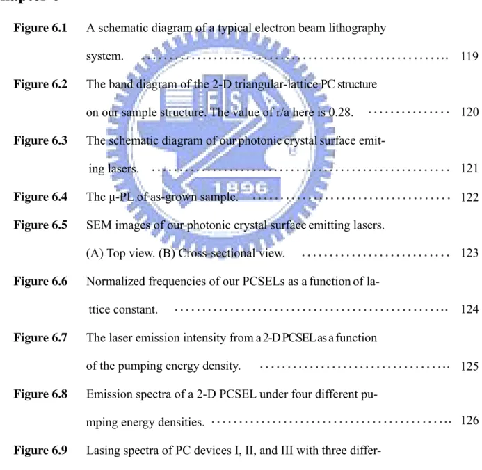
Figure 1.1 The band-gap diagram of II-VI and III-V semiconductor
materials.
Figure 1.2 The schematic diagram of an edge emitting laser diode. Figure 1.3 The Schematic diagram of a vertical-cavity emitting laser
diode.
Figure 1.4 Schematic diagrams of three nitride-based VCSEL structures Figure 1.5 The band diagram of a 2-D triangular-lattice PC structure.
Chapter 2
Figure 2.1 An illustration of output power vs. current for a diode
laser .
Figure 2.2 A schematic diagram of DBRs
Figure 2.3 The internal photon numbern versus the pump rate0 P as
a function of a spontaneous emission coefficientβ .
Figure 2.4 (A) The band diagram of a triangular-lattice photonic cry-
stal. (B) The schematic diagram of a reciprocal space.
Figure 2.5 Wave-vector diagrams at (A) point I, (B) point II, and (C)
point III. ki and kd indicate incident and diffracted wave ve-
ctor.
Figure 2.6 The wave-vector diagram at point III in vertical direction.
Chapter 3
16 15 12 32 31 34 33 35 36 14 13……
………
………
…………
………
………
……
……
………
………
………
XIII
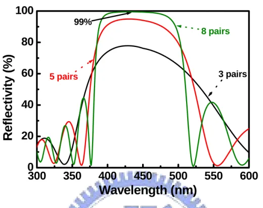
Figure 3.1 Simulated reflectivity spectra of 5, 10, 15, and 25 pairs
of AlN/GaN DBR.
Figure 3.2 Simulated reflectivity spectra of three different nitride -
based DBRs with high reflectivity.
Figure 3.3 Simulated reflectivity spectra of 3, 5, and 8 pairs of
Ta2O5/SiO2 DBR.
Figure 3.4 Electric field intensity and refractive index as a function
of the distance from top layer.
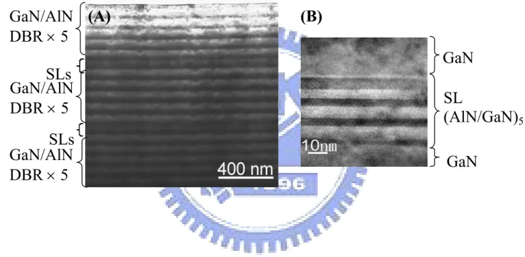
Figure 3.5 Cross-sectional TEM images of (A) the DBR sample and
(B) one set of 5.5 pairs of GaN/AlN SL insertion layers.
Figure 3.6 AFM image of the DBR sample. Figure 3.7 The reflectivity spectrum of the AlN/GaN DBR. Figure 3.8 (A) OM and (B) cross-sectional TEM images of the as-
grown micro-cavity sample.
Figure 3.9 The reflectivity spectrum of the Ta2O5/SiO2 DBR.
Figure 3.10 (A) Schematic diagram, (B) SEM image, and (C) OM
images of the VCSEL structure.
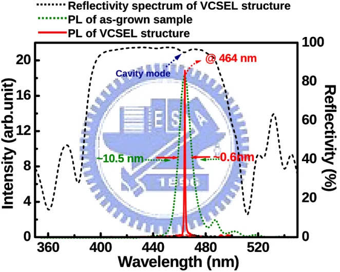
Figure 3.11 PL emission of as-grown structure and VCSEL structure,
and the reflectivity spectrum of VCSEL structure.
Figure 3.12 The optical pumping setup. Figure 3.13 The light emission intensity of VCSEL as afunctionofthe
pumping energy.
Figure 3.14 Emission spectra of VCSEL under different pumping
energy.
Figure 3.15 Emission images of nitride-based VCSEL under different
pumping energy. 60 59 59 58 56 55 54 53 49 49 57 52 51 50 50
………
………
………
………
………
………
…………
………
………
………
………
………
………
………
………
Figure 3.16 The laser emission intensity of VCSEL as afunctionofthe
angle of the polarizer at the pumping energy of 1.71Eth.
Figure 3.17 (A) Near-field intensity distribution and (B) Far-field
emission pattern of the laser spot.
Figure 3.18 Semi natural-logarithm plot of the dependence of the
threshold pumping energy (lnEth) on the operation temperature.
Figure 3.19 The lasing wavelength of nitride-based VCSEL as a
function of temperature.
Figure 3.20 The center wavelength of AlN/GaN DBR asafunctionof
temperature.
Figure 3.21 Photon numbers as a function of pump ratio. The solid
lines are fitting curves with β values of 0.02, 0.025, and
0.03, and the dots are experiment data.
Chapter 4
Figure 4.1 The PL intensity distribution of one region on the as-
grown sample with a scanning area of 20× 20 μm2.
Figure 4.2 (A) The wavelength distribution of the regionshownin
figure 4.1. (B) The PL spectrum of the dotted circleand
the reflectivity spectrum of the region.
Figure 4.3 Emission images of multiple laser spots under four
different pumping energy of 0.8 Eth, 1.1Eth, 1.3Eth, and
1.4Eth.
Figure 4.4 Emission spectra of multiple laser spots under four
76 75 74 66 65 64 63 61 62
……….
………
………
………
………
………
………
………
………
XV
different pumping energy of 0.8 Eth, 1.1Eth, 1.3Eth, and
1.4Eth.
Figure 4.5 Four observed lasing emission images and intensity
distributions simialr to TEM00, TEM01, TEM02
and TEM11 in the four different regions.
Figure 4.6 The threshold characteristic of pumping region I on GaN
VCSEL sample.
Figure 4.7 The threshold characteristic of pumping region II on GaN
VCSEL sample.
Figure 4.8 Emission spectra of the pumping region I underdifferent
pumping energy.
Figure 4.9 Emission spectra of the pumping region II under different
pumping energy.
Figure 4.10 Emission spectra of nitride-based VCSEL emitting two
kinds of mode patterns, similar to TEM01 and TEM11 at
the same region with the same pumping energy.
Figure 4.11 PL Emission intensity distributions of four pumping
regions shown in figure 4.5.
Figure 4.12 PL spectra of three places marked in the photo shown in
the inset. The inset is PL emission image of theregion
emitting TEM01.
Chapter 5
Figure 5.1 Transmission (T) and reflectivity (R) versus wavelength
85 84 82 81 80 79 78 77 83
………
………
………
………
………
………
………
………
……….
of Ni/Au (5/5nm) and ITO (300nm) films deposited
on glass substrate.
Figure 5.2 Electric field intensity and refractive index as a function
of the distance from top layer.
Figure 5.3 The process flowchart of nitride-based micro-cavity devices. Figure 5.4 The current-voltage characteristic of ITO contact. Figure 5.5 The schematic diagram of a fabricated micro-cavity light
emitting diode.
Figure 5.6 SEM images of the fabricated device. (A) Top view. (B)
Cross-sectional view.
Figure 5.7 The probe station measurement setup.
Figure 5.8 Current versus voltage and light output power curves of
a fabricated device at room temperature.
Figure 5.9 (A) Emission images under different injection current.
(B)A MCLED chip monted on a metal can.
Figure 5.10 Emission spectra of the MCLED under different current
of 3 mA, 6 mA, and 10 mA.
Figure 5.11 The variation of emission (A)linewidth and(B)wavelength
of the MCLED with increasing current.
Figure 5.12 Emission peak wavelength of the MCLED as a function
of temperature.
Figure 5.13 (A) The simulation and (B) SIMS data of Mg+ ion
distribution inside the implanted sample with 100nm-thick SiNx buffer layer.
Figure 5.14 OM image of the implanted sample. Figure 5.15 (A) Emission images of Mg+ implanted MCLEDs after
107 106 105 104 103 102 101 100 99 98 96 95 108 97
………
………
………
………
………
………
………
………
………
………
………
………
………
………
XVII
deposition of ITO transparent contact layer. (B) Emission
image of MCLED with aperture size of 40μm in high
magnification.(C)Emission image of fabricated implanted MCLED.
Figure 5.16 Current-voltage curves of the conventional andthe Mg+-
implanted MCLEDs.
Chapter 6
Figure 6.1 A schematic diagram of a typical electron beam lithography
system.
Figure 6.2 The band diagram of the 2-D triangular-lattice PC structure
on our sample structure. The value of r/a here is 0.28.
Figure 6.3 The schematic diagram of ourphotoniccrystalsurface emit-
ing lasers.
Figure 6.4 The μ-PL of as-grown sample. Figure 6.5 SEM images of our photonic crystal surfaceemitting lasers.
(A) Top view. (B) Cross-sectional view.
Figure 6.6 Normalized frequencies of our PCSELs as afunctionof la-
ttice constant.
Figure 6.7 The laser emission intensity from a 2-D PCSEL as a function
of the pumping energy density.
Figure 6.8 Emission spectra of a 2-D PCSEL under four different pu-
mping energy densities.
Figure 6.9 Lasing spectra of PC devices I, II, and III with three differ-
ent lattice constants, 201 nm, 244 nm, and 290nm, respec-
126 125 124 123 122 121 120 119 110 109
………..
………..
………..
………
………
………
………
………..
………
……….
tively.
Figure 6.10 The comparison of simulated PC band diagram (figure 6.2)
and experiment data (figure 6.6).
Figure 6.11 (A) The spontaneous emission image at 0.92Eth ( pumping
spot size was about 50μm) and (B) Laser emission image at 1.47Eth.
Figure 6.12 The laser emission intensity of a PCSEL as a functionof the
angle of the polarizer.
Figure 6.13 The laser emission intensity of a PCSEL as a functionof the
detecting angle of the fiber.
Chapter 7
Figure 7.1 Schematic diagram of a photonic crystal surface emitting laser
131 130 129 128 127 137
………
……….
………
………..
……….
………
1
Chapter 1
Introduction
1-1 Wide-bandgap III-N materials
Wide-bandgap nitride materials have attracted great attention over past decade due to their promising potential for the applications of optoelectronic devices such as flat panel display, competing storage technologies, automobiles, general lighting, and biotechnology, and so on [1-4]. The III-N materials are synthesized mainly using the four kinds of atoms, gallium (Ga), nitride (N), aluminum (Al), and indium (In), to form the binary and ternary
compunds such as GaN, InN, AlN, InxGa1-xN, and AlxGa1-xN etc. The bandgap of these
materials cover a very wide range from 0.9eV to 6.1eV (figure 1.1), which implies the large band off-set in hetero-structure could be achieved in this material system. The large band off-set is very useful to confine carrier for the high-speed and high power electronic devices and light emitting devices [5]. Their wide-range bandgap also provide possibility of full-color emission because they cover red, green, and blue emission regions. This property further makes nitride materials important and important for the applications of full-color display or solid-state lighting. Furthermore, nitride materials still have lots of advantages such as high
bond energy (~2.3eV), high saturation velocity (~2.7× 104 cm/s), high breakdown field
(~2× 10⁶ V/cm), and strong excitonic energy (>50meV)[6-7]. Although wurtzite nitride compounds have some unique properties such as piezoelectric field and spontaneous polarization which is harmful to the efficiency of light emitting devices, the material system still is a very strong candidate for the future optoelectronic applications due to their superior material properties.
The research of blue light emitting devices began from the development of gallium nitride light emitting diodes in the early 1970s [8-10]. Two decades later, with several efforts devoted to the growth of nitride materials, doping concentration, efficiency of quantum wells, and so on, Nakamura et. al. [2] developed the first prototype high-brightness (>100 times greater than previous alternatives, about 1 candela) GaN blue light emitting diodes in 1993. Then, in 1995, they also developed the first successful GaN electron-injection laser [1]. This makes nitride laser diodes begin to step on the road toward the commercial applications of high-information-density storage, laser printer, compact projector, and etc. In these years, the performance of nitride laser diodes has been improved to emit power as high as 100mW at room temperature with a low threshold only 3 kA/cm2 [11], and the devices have been already successfully commercialized to be applied to digital versatile disc (DVD). This next-generation DVD would enlarge the storage capacity from 4.7 giga-bytes which current DVD owns to 27 giga-bytes.
1-2.1 Edge emitting lasers
The major type of commercial nitride-based laser diodes now is edge emitting laser. This kind of structure is currently the most mature and producible one among all nitride laser devices. It is featured by a stripe-type long cavity and a pair of cleaved facet as the mirrors as shown in figure 1.2. Typically, the cavity length of the structure is about several hundred micro-meters. The light in the cavity is resonant in the horizontal direction and emits from the cleaved mirrors. The standard epi-layer structure of EELs usually is grown on sapphire and composes of p-n junction, multiple quantum wells (active region), and some cladding layer for photons and electrons. Over this decade, several improvements and researches on the growth and optimization of its structure were reported [12-15]. One is to improve the great amounts of defects and threading dislocations existing in the grown nitride materials on sapphire substrate due to the large lattice-mismatch between the nitride material and sapphire.
3
The epitaxally lateral overgrowth (ELOG) is a very efficient method to reduce threading dislocation and defect density [12, 13]. It is a method using the patterned SiOx to make GaN laterally coalesce and bend threading dislocations to reduce the dislocation density. Generally, ELOG could decrease dislocation density down to the order of 108 cm-2. Other one is to raise the low confinement factor of the optical field in the structure. Because the index difference between AlxGa1-xN and GaN is small, the guiding of optical field in active region is usually
weak. Nakamura et. al. provided a solution that using modulation doped strain superlattice
layer to improve the optical confinement [12, 13]. The other is to reduce spontaneous
polarization and piezoelectric field in multiple quantum wells. Recently, M. Schmidt et. al. [14] and D. Feezell [15] et. al. demonstrated nonpolar laser diode on m-plane GaN substrate. The laser diode emits violet light ~410nm and has the threshold current density of 3.7-8.2 KA/cm2. The spontaneous and piezoelectric polarization effect was eliminated and the performance of laser diode could be further improved using this lattice matched substrate. The fabrication of flat and high-reflectivity mirrors is also a key point for achieving an excellent lasing performance. In order to obtain a flat facet, the etching and cutting techniques were rapidly developed.
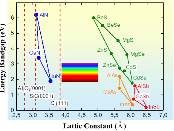
1-2.2 Vertical Surface Emitting Lasers
Although the optimization of the edge emitting laser keeps going, some properties of this kind of laser are unfavorable. One of those properties is its elliptic beam shape. On one hand, the coupling efficiency would be low as the elliptic beam is coupled into optical fiber (typically in the form of circular core). On the other hand, for the application of storage, the elliptic beam not only makes each writing pixel larger but also raises expenses for correcting light shape. Usually, this kind of laser shows slightly large divergence angle to be over ten degree. This also is disadvantageous to the projection. Furthermore, the side emitting laser devices also makes the testing of devices a tough task. The wafer should be cut into several
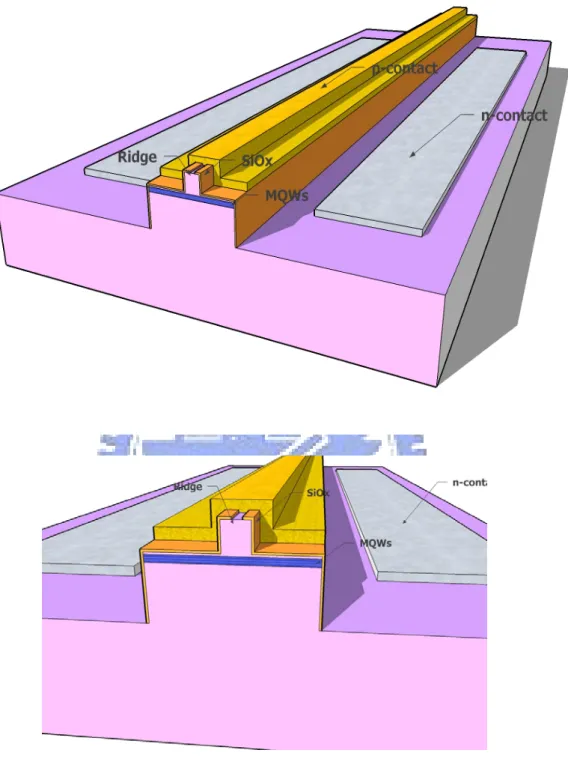
stripes (several laser devices on one strip) before the testing. For a commercial product, the complicated testing would result in a poor producing efficiency and be disadvantageous. Therefore, in order to have a superior laser device, K. Iga [16] demonstrated a new kind of laser diodes, vertical cavity surface emitting laser, in 1977. Vertical cavity surface emitting laser (VCSEL) is a vertical-emitting-type laser. It is formed by sandwiching a few-lambda cavity in a pair of reflectors, usually in the form of distributed Bragg reflector (DBR), with a very high reflectivity (>99.9%) (as shown in figure 1.3). In contrast to EELs, photons in the cavity of VCSEL are vertically in resonance and emit outside perpendicularly to the surface of the structure. This laser diode can have many advantageous properties than conventional edge emitting laser, such as circular beam shape, lower divergence angle, two-dimensional laser array possible, efficient testing, low threshold, and so on. Owing to these superior performances, VCSELs had become very attractive and started to be applied to the commercial products at long wavelength range. In fact, short-wavelength VCSELs are also very promising for the applications of storage, display, and projection. In particular, the use of two-dimensional arrays of blue VCSELs could further reduce the read-out time in high density optical storage and increase the scan speed in high-resolution laser printing
technology [17]. In recent years, several efforts have been devoted to the realization of
nitride-based VCSELs [18-27]. Currently, three kinds of structures were reported:
I. Fully epitaxial grown VCSEL structure
In 2005, J. F. Carlin [26] and E. Feltin [27] demonstrated the wholly epitaxial and high quality nitride-based micro-cavity (as shown in figure 1.4(A)) using metalorganic vapor phase epitaxy (MOVPE or MOCVD). They used the lattice-matched AlInN/GaN as the bottom and top reflectors to avoid cracks happened due to the accumulation of the strain after stacking large pairs of layers. The reflectivity of AlInN/GaN could be achieved as high as 99.4%. They showed the 3/2-lambda cavity emitted a very narrow emission with a linewidth of 0.52 nm, corresponding to a quality factor of ~800.
5 II. VCSEL structure with two dielectric mirrors
Compared to epitaxial grown reflectors, the fabrication of dielectric mirrors is relatively simple. Furthermore, the large index difference of dielectric mirrors makes them could easily have wide stop band (>50nm) and high reflectivity (>99%) by coating just few stacks of 1/4-lambda-thick layers. Therefore, using dielectric mirrors to accomplish nitride-based VCSELs had begun attractive. Song et al. [19], Tawara et al. [20] and J. T. Chu et. al. [22] successively reported the structure (as shown in figure 1.4(B)) after 2000. They employed some process techniques such as wafer bonding and laser lift-off to make dielectric mirrors be coated onto both sides of nitride-based cavity. They showed a micro-cavity could have a very high quality factor to be greater than 400 and achieve lasing action using optical pumping.
III. VCSEL structure with hybrid mirrors
The so-called hybrid mirrors are a combination of two different kinds of reflectors, for example, a dielectric mirror and an epitaxial reflector. Typically, the fabrication of this structure is to grow bottom reflector and cavity using MOCVD and then coat dielectric mirror to complete VCSEL structure (as shown in figure 1.4(C)). The hybrid-cavity nitride-based VCSEL\formed by the dielectric mirror and the epitaxially grown high-reflectivity
GaN/AlxGa1-xN DBR was reported earlier. In 1999, Someya et al. [18] used 43 pairs of
Al0.34Ga0.66N/GaN as the bottom DBR and reported the lasing action at ~400nm. Then, Zhou
et al [21] also employed a bottom DBR of 60 pairs Al0.25Ga0.75N/GaN and observed the lasing
action at 383.2nm. Both these AlGaN/GaN DBR structures required large numbers of pairs due to the relatively low refractive index contrast between AlxGa1-xN and GaN. Therefore,
recently some groups began to study the AlN/GaN for application in nitride VCSEL. The
DBR structure using AlN/GaN has higher refractive index contrast (Δn/n=0.16)[28] that can
achieve high reflectivity with relatively less numbers of pairs. It has wide stop band that can easily align with the active layer emission peak to achieve lasing action. However, the AlN/GaN combination also has relatively large lattice mismatch (~2.4%) and the difference in
thermal expansion coefficients between GaN (5.59x10⁻⁶/K) and AlN (4.2x10⁻⁶/K) that tends to cause cracks in the epitaxial film during the growth of the AlN/GaN DBR structure and could result in the reduction of reflectivity and increase in scattering loss. With the mature of epitaxy techniques, the high-reflectivity AlN/GaN DBR structure with relatively smooth surface morphology has become possible with just twenty or thirty pairs [29].
In comparison of these three VCSELs, it doesn’t require complicated process such as laser lift-off technique to complete a hybrid VCSEL device. This means the fabrication of such structure is stable and reliable comparing to other structures. Thus, the hybrid structure is more advantageous in the aspects of fabrication and commercialization
In fact, the investigation of the characteristics of the GaN-based VCSELs has gradually attracted more attentions. Kako et al. [30] investigated the coupling efficiency of spontaneous emission (β) and the polarization property of the nitride VCSEL and obtained a high β value of 1.6×10⁻² and a strong linear polarization of 98%. Tawara et al. [20] also found a high β value of 10-2 in the nitride VCSEL with two dielectric mirrors. Honda et al. reported the estimation of high characteristics temperature of GaN-based VCSEL [31]. These all mean the development of nitride-based VCSEL and the understanding of the laser performance has become more and more important. Especially, the current-injected nitride-based VCSEL still can’t be realized, therefore, more efforts on it are necessary and crucial for high performance future application.
1-2.3 Two-dimensional (2-D) photonic crystal lasers
Besides VCSEL, a novel structure, photonic crystal (PC) laser, was demonstrated to be a new type of the vertical emitting laser after 1990s. It is featured by a periodic structure called photonic crystal. According to the theory, the light in the photonic crystal structure would be forbidden or only allowed in specific modes, and those modes could be plotted as a photonic band diagram as shown in figure 1. 5. Consequently, such structures can act not only as a
7
passive waveguide or resonator to direct the wave propagation but also as an active medium to control light emission [32]. For fabricating laser devices, there are two kinds of 2-D PC lasers to be reported in these few years. One is 2-D PC nano-cavity laser, and another is 2-D PC band-edge laser.
I. 2-D PC Nano-Cavity Lasers
In 1994, P. R. Berman et al. first presented that photonic crystal could be a reflective
mirror around the cavity of a laser [33]. Then, in 1999 O. Painter practically demonstrated an optically pumped InGaAs-based 2-D PC nano-cavity laser emitting 1.55 micrometers (as
shown in figure 1.6.1) [34]. The optical cavity he demonstrated consisted of a
half-wavelength-thick waveguide for vertical confinement and a 2-D PC mirror for lateral localization. A defect was introduced as a nano-cavity (a volume of 2.5 cubic half-wavelength, approximately 0.03 cubic micrometers) in the 2-D PC to trap photons inside. In 2004, Hong-Gyu Park et al. realized the electrically driven single-cell 2D-PC laser (λ=1519.7 nm)
[35]. They used a sub-micrometer-sized semiconductor post placed below the center of the
single-cell photonic crystal resonator to connect bottom electrode and achieved lasing action via current injection.
In 2005, nitride-based blue (about 488nm) photonic crystal membrane nano-cavity with
Q factor about 800 was also reported by Y. S. Choi et al. [36]. They used photo-enhanced
chemical etching to form a GaN membrane with a total thickness of 140 nm and patterned a photonic crystal cavity on it. Some resonance modes from the nano-cavities with lattice constant 180 nm could be observed in the photoluminescence (PL) emission.
II. 2-D PC Band-edge lasers
Compared to 2-D PC nano-cavity lasers, it is not necessary to create a defect in the 2-D photonic crystal to be a nano-cavity for a 2-D PC band-edge laser. That is, the 2-D photonic band-edge laser is composed of a perfect photonic crystal structure. Then, by satisfying Bragg condition, the laser action would happen in those band edge points in the photonic band
diagram. In 1999, Noda et al. reported the electrically driven 2-D PC band-edge laser under pulsed operation [37]. The PC was a triangular-lattice structure composed of InP and air holes, which is integrated with an InGaAsP/InP multiple-quantum-well active layer by a wafer fusion technique. They demonstrated the single-mode, large-area and surface-emitting lasing action, and analyzed the lasing mechanism based on the satisfying of Bragg condition. Then, they further reported the room-temperature (RT) 2-D PC band-edge laser under continuous
wave (CW) operation in 2004 [38]. This opens a new road toward the large-area single-mode
surface emitting laser.
1-3 Objectives of this thesis
From the view of superior laser devices, the single mode, large area, high output-power, and surface emitting have become basic requirements for the future laser device. In this thesis, we mainly focus on the study of nitride-based surface emitting lasers including the vertical-cavity surface emitting laser and 2-D PC surface emitting laser. The study of nitride-based VCSELs consists of the design, fabrication, and characteristics of the laser. We discuss and analyze the performance of nitride-based VCSEL such as threshold characteristics, laser spectrum, polarization, divergence angle, characteristic temperature, and coupling efficiency of spontaneous emission. Furthermore, unique lasing phenomenon, such as specific mode behavior and multiple-spot lasing, of the nitride-based VCSEL resulting from the inhomogeneity of gain and quality factor in the structure are also investigated. We also establish the fabrication processes of nitride-based vertical-cavity surface emitting devices and put the VCSEL structure into the processes to get a high-quality surface emitting device. Besides, we develop the other surface emitting laser, 2-D PC surface emitting laser, using the epitaxial part of our nitride-based VCSEL, i. e. the structure with a nitride cavity and a nitride bottom reflector. The fabrication and characteristics of the nitride-based 2-D PC surface emitting laser are also demonstrated and investigated.
9
References
1. S. Nakamura, M. Senoh, N. Iwasa, and S. Nagahama, Jpn. J. Appl.Phys., 34, L797 (1995) 2. S. Nakamura, T. Mukai, and M. Senoh, Appl. Phys. Lett.,64, 1687 (1994)
3. S. Nakamura, M. Senoh, S.Nagahama, N.Iwasa, T. Yamada, T. Matsushita, Y. Sugimoto, and H.Kiyoku, Appl. Phys. Lett., 70, 868 (1997)
4. S. Nakamura, Science, 281, 956 (1998)
5. Y. Arakawa, IEEE J. Select. Topics Quantum Electron., 8, 823 (2002)
6. H. Morkoc, Nitride Semiconductors and Devices (Spring Verlag, Heidelberg) (1999) 7. S. N. Mohammad, and H. Morkoc, Progress in Quantum Electron., 20, 361 (1996) 8. J. I. Pankove, E. A. Miller, J. E. Berkeyheier, J. Luminescence, 5, 84 (1972) 9. H. P. Maraska, D. A. Stevenson, J. I. Pankove, Appl. Phys. Lett., 22, 303 (1973) 10. J. I. Pankove, Phys. Rev. Lett., 34, 809 (1975).
11. M. Takeya, T. Tojyo, T. Asano, S. Ikeda, T. Mizuno, O. Matsumoto, S. Goto, Y. Yabuki, S. Uchida, and M. Ikeda, phys. stat. sol. (a), 192, 269 (2002)
12. S. Nakamura, M. Senoh, S. Nagahama, N. Iwasa, T.Yamada, T. Matsushita, H. Kiyoku, Y. Sugimoto, T. Kozaki, H. Umemoto, M. Sano, and K. Chocho, Appl. Phys. Lett., 72, 211 (1998)
13. S. Nakamura, IEEE J. Select. Topics Quantum Electron., 4, 483 (1998)
14. M. C. Schmidt, K. C. Kim, R, M. Farrell, D. F. Feezell, D. A. Cohen, M. Saito, K. Fujito, J. S. Speck, S. P. Denbaars, and S. Nakamura, Jpn. J. Appl. Phys, 46, L190 (2007)
15. D. F. Feezell, M. C. Schmidt, Robert M. Farrell, K. C. Kim, M. Saito, K. Fujito, D. A. Cohen, J. S. Speck, S. P. Denbaars, and S. Nakamura, Jpn. J. Appl. Phys, 46, L284 (2007) 16. K. Iga, IEEE J. Quantum Electron., 24, 1845 (1988)
17. K.Iga, Proceedings of the First International Symposium on blue lasers and light emitting
diodes, Th-11 (1996)
1905 (1999)
19. Y.-K. Song, H. Zhou, M. Diagne, A. V. Nurmikko, R. P. Schneider, Jr., C. P. Kuo, M. R. Krames, R. S. Kern, C. Carter-Coman, and F. A. Kish, Appl. Phys. Lett., 76, 1662 (2000) 20. T. Tawara, H. Gotoh, T. Akasaka, N. Kobayashi, and T. Saitoh, Appl. Phys. Lett., 83, 830
(2003)
21. H. Zhou, M. Diagne, E. Makarona, A. V. Nurmikko, J. Han, K. E. Waldrip and J. J. Figiel,
Electron. Lett., 36,1777 (2000)
22. J.T. Chu et. al., Jpn. J. Appl. Phys, 45, 2556 (2006). 23. J. T. Chu et. al., Appl. Phys. Lett., 89, 121112 (2006). 24. C. C. Kao et. al., Appl. Phys. Lett., 87, 081105-1 (2005). 25. C. C. Kao et. al., IEEE Photon. Technol. lett., 18, 877 (2006).
26. J. F. Carlin, J. Dorsaz, E. Feltin, R. Butté, N. Grandjean, M. Ilegems, and M. Laügt, Appl.
Phys. Lett., 86, 031107 (2005)
27. E. Feltin, R. Butté, J. F. Carlin, J. Dorsaz, N. Grandjean, and M. Ilegems, Electron. Lett.,
41, 94 (2005)
28. T. Ive, O. Brandt, H. Kostial, T. Hesjedal, M. Ramsteiner, and K. H. Ploog, Appl. Phys.
Lett., 85, 1970 (2004)
29. H.H. Yao, C.F. Lin, H.C. Kuo, S.C. Wang, J. Crystal Growth, 262, 151 (2004) 30. S. Kako, T. Someya, and Y. Arakawa, Appl. Phys. Lett., 80, 722 (2002)
31. T. Honda, H. Kawanishi, T. Sakaguchi, F. Koyamaand K. Iga, MRS Internet J. Nitride
Semicond. 4S1, G6.2-1 (1999).
32. C. M. Lai, H. M. Wu, P. C. Huang, S. L. Peng, Appl. Phys. Lett., 90, 141106, (2007) 33. P. R. Berman, New York:Academic, (1994)
34. O. Painter, R. K. Lee, A. Scherer, A. Yariv, J. D. O`Brien, P. D. Dapkus, I. Kim, Science,
284, 1819, (1999)
11
Science, 305, 1444, (2005)
36. Y. S. Choi, K. Hennessy, R. Sharma, E. Haberer, Y. Gao, S. P. DenBaars, C. Meier, Appl.
Phys. Lett., 87, 243101, (2005)
37. M. Imada, S. Node, A. Chutinan. and T. Tokuda, Appl. Phys. Lett., 75, 316, (1999) 38. D. Ohnishi, T. Okano, M. Imada, and S. Node, Opt. Exp., 12, 1562, (2004)
Figure 1.1 The band-gap diagram of II-VI and III-V semiconductor
materials.
Lattic Constant (
A
o)
Energy Bandgap
13
Figure 1.3 The schematic diagram of a vertical-cavity emitting laser
diode.
15
Figure 1.4 Schematic diagrams of three nitride-based VCSEL structures.
epitaxial
mirror
epitaxial
mirror
Cavity
epitaxial
mirror
epitaxial
mirror
Cavity
(A)
dielectric
mirror
dielectric
mirror
Cavity
dielectric
mirror
dielectric
mirror
Cavity
(B)
dielectric
mirror
epitaxial
mirror
Cavity
dielectric
mirror
epitaxial
mirror
Cavity
(C)
0.0
0.1
0.2
0.3
0.4
0.5
0.6
0.7
0.8
N
o
rm
a
liz
e
d
f
re
q
u
e
n
c
y
(
a
/
λ
)
Γ
M K
Γ
17
Chapter 2
Fundamentals of Micro-Cavity Surface Emitting Lasers
2-1 Operation Mechanism of Semiconductor Lasers
[1-7]Carrier density rate equation
For the DH active region, the injected current provides a generation term, and various radiative and nonradiative recombination process as well as carrier leakage provide recombination terms. Thus, we can write the carrier density rate equation,
where N is the carrier density (electron density), Ggen is the rate of injected electrons and Rrec
is the ratio of recombining electrons per init volume in the active region. Since there areηi I/q
electrons per second being injected into the active region,
qV I G i
gen
η
= , where V is the volume
of the active region. The recombination process is complicated and several mechanisms must
be considered. Such as, spontaneous recombination rate, Rsp ~ BN2, nonradiative
recombination rate, Rnr, carrier leakage rate, Rl, (Rnr + Rl = AN+CN3), and stimulated
recombination rate, Rst. Thus we can write Rrec = Rsp + Rnr + Rl +Rst. Besides, N/τ ≡ Rsp + Rnr
+ Rl, where τ is the carrier lifetime. Therefore, the carrier density rate equation could be
expressed as
Photon density rate equation
Now, we describe a rate equation for the photon density, Np, which includes the photon
generation and loss terms. The photon generation process includes spontaneous recombination (Rsp) and stimulated recombination (Rst), and the main photon generation term of laser above
rec gen R G dt dN − = (2.01) st i N R qV I dt dN − τ − η = (2.02)
threshold is Rst. Every time an electron-hole pairs is stimulated to recombine, another photon
is generated. Since, the cavity volume occupied by photons, Vp, is usually larger than the
active region volume occupied by electrons, V, the photon density generation rate will be [V/Vp]Rst not just Rst. This electron-photon overlap factor, V/Vp, is generally referred to as the
confinement factor, Γ. Sometimes it is convenient to introduce an effective thickness (deff),
width (weff), and length (Leff) that contains the photons. That is, Vp=deffweffLeff. Then, if the
active region has dimensions, d, w, and La, the confinement factor can be expressed as,
Γ=ΓxΓyΓz, whereΓx = d/deff, Γy = w/weff, Γz = La/Leff. Photon loss occurs within the cavity due
to optical absorption and scatting out of the mode, and it also occurs at the output coupling mirror where a portion of the resonant mode is usually couple to some output medium. These net losses can be characterized by a photon (or cavity) lifetime, τp. Hence, the photon density
rate equation takes the form
where βsp is the spontaneous emission factor. As to Rst, it represents the photon-stimulated net
electron-hole recombination which generates more photons. This is a gain process for photons. It is given by
where vg is the group velocity and g is the gain per unit length.
Now, we rewrite the carrier and photon density rate equations
Threshold gain p p sp sp st p N R R dt dN τ − β Γ + Γ = (2.03) p g p st gen p N v t N R dt dN g = Δ Δ = = ⎟⎟ ⎠ ⎞ ⎜⎜ ⎝ ⎛ (2.04) p g i N v N qV I dt dN g − τ − η = p p sp sp p g p N R N v dt dN τ − β Γ + Γ = g (2.05) (2.06)
19
In order for a mode of the laser to reach threshold, the gain in the active section must be increased to the point when all the propagation and mirror losses are compensated. Most laser cavities can be divided into two general sections: an active section of length La and a passive
section of length Lp. For a laser, at the threshold, the gain is equal whole loss in the cavity,
which includes cavity absorption and mirror loss. For convenience the mirror loss term is sometimes abbreviated as, αm ≡ (1/2L) ln(1/R1R2). Noting that the cavity life time (photon
decay rate) is given by the optical loss in the cavity, 1/τp = 1/τi + 1/τm = vg(αi +αm). Thus, the
threshold gain in the steady state can be expressed with following equation
where αi is the average internal loss which is defined by (αiaLa + αipLp)/L (i.e.,αiaLa andαipLp
are loss of active region and passive section, respectively), and R1 and R2 is the reflectivity of
top and bottom mirror of the laser cavity, respectively.
Output power versus driving current
The characteristic of output power versus driving current (L-I characteristic) in a laser diode can be realized by using the rate equation Eq. (2.05) and (2.06). Consider the below threshold (almost threshold) steady-state (dN/dt = 0) carrier rate equation, the Eq. (2.05) is given by τ = ηi th Nth qV I
. While the driving current is above the threshold, the carrier rate equation will be
From Eq. (2.08), the steady-state photon density above threshold where g = gth can be
calculated as ⎟⎟ ⎠ ⎞ ⎜⎜ ⎝ ⎛ + α = τ = α + α = Γ 2 1 i p g m i R R 1 ln L 2 1 v 1 th g (2.07) p g th i v N qV ) I I ( dt dN g − − η = (2.08) V qv ) I I ( N th g th i p g − η = (2.09)
The optical energy stored in the cavity, Eos, is constructed by multiplying the photon density,
Np, by the energy per photon, hν, and the cavity volume, Vp. That is Eos = NphνVp. Then, we
multiple this by the energy loss rate through the mirrors, vgαm = 1/τm, to get the optical power
output from the mirrors, P0 = vgαmNphνVp. By using Eq. (2.07) and (2.09), and Γ=V/Vp, we
can write the output power as the following equation
Now, by defining m i m i d α α α η =
η , the Eq. (2.10) can be simplified as
Thus, the ηd can be expressed as
In fact, ηd is the differential quantum efficiency, defined as number of photons out per electron.
Besides, dPo/dI is defined as the slope efficiency, Sd, equal to the ratio of output power and
injection current. Figure 2.1 shows the illustration of output power vs. current for a diode laser. Below threshold only spontaneous emission is important; above threshold the stimulated emission power increase linearly with the injection current, while the spontaneous emission is clamped at its threshold value.
2-2 Penetration Depth of Distributed Bragg Reflectors
[8-13]Distributed Bragg reflectors (DBRs) served as high reflecting mirror in numerous optoelectronic and photonic devices such as VCSEL. It is a periodic structure formed by stacking several pairs of two 1/4-lamda-thick layers with different refractive index. Consider a distributed Bragg reflector consisting of m pairs of two dielectric, lossless materials with
) I I ( q h P th m i m i O − ν ⎟⎟ ⎠ ⎞ ⎜⎜ ⎝ ⎛ α + α α η = (2.10) ) I I ( q h PO =ηd ν − th (I > Ith) (2.11) dI dP h q O d ⎥⎦ ⎤ ⎢⎣ ⎡ ν = η (I > Ith) (2.12)
21
high- and low- refractive index nH and nL, as shown in figure 2.2. The thickness of the two
layers is assumed to be a quarter wave, that is, L1 =λB/4nH and L2 =λB/4nL, where the λB is the
Bragg wavelength.
Multiple reflections at the interface of the DBR and constructive interference of the multiple reflected waves increase the reflectivity with increasing number of pairs. The
reflectivity has a maximum at the Bragg wavelength λB. The reflectivity of a DBR with m
quarter wave pairs at the Bragg wavelength is given by
where the no and ns are the refractive index of incident medium and substrate.
The high-reflectivity or stop band of a DBR depends on the difference in refractive index of the two constituent materials, △n (nH-nL). The spectral width of the stop band is given by
where neff is the effective refractive index of the mirror. It can be calculated by requiring the
same optical path length normal to the layers for the DBR and the effective medium. The effective refractive index is then given by
The length of a cavity consisting of two metal mirrors is the physical distance between the two mirrors. For DBRs, the optical wave penetrates into the reflector by one or several quarter-wave pairs. Only a finite number out of the total number of quarter-wave pairs are effective in reflecting the optical wave. The effective number of pairs seen by the wave electric field is given by
(2.13) (2.14) (2.15) (2.16) ⎟ ⎟ ⎟ ⎟ ⎠ ⎞ ⎜ ⎜ ⎜ ⎜ ⎝ ⎛ + − = p 2 p 2 ) n n ( n n 1 ) n n ( n n 1 R H L o s H L o s eff B stopband n n 2 π Δ λ = λ Δ 1 eff ) n 1 n 1 ( 2 n L H − + = ) n n n n m 2 tanh( n n n n 2 1 m L H L H L H L H eff + − − + ≈
For very thick DBRs (m→∞) the tanh function approaches unity and one obtains
Also, the penetration depth is given by
where r = (n1-n2)/ (n1+n2) is the amplitude reflection coefficient.
For a large number of pairs (m→∞), the penetration depth is given by
Comparison of Eqs. (2.17) and (2.19) yields that
The factor of (1/2) in Eq. (2.20) is due to the fact that meff applies to effective number of
periods seen by the electric field whereas Lpen applies to the optical power. The optical power
is equal to the square of the electric field. The effective length of a cavity consisting of two DBRs is thus given by the sum of the thickness of the center region plus the two penetration depths into the DBRs.
2-3 Coupling Efficiency of Spontaneous Emission into a Lasing Mode
[14]In a conventional semiconductor laser, only a very small part of the spontaneous emission is coupled into a single-lasing mode. That is because the radiation pattern of spontaneous emission is isotropic, a substantial part of the spontaneous emission is not coupled to the guided modes in an active waveguide with a small acceptance angle. Furthermore, the spontaneous emission spectral linewidth is broader than the linewith of the
(2.17) (2.18) (2.19) (2.20) L H L H n n n n 2 1 meff − + ≈ ) mr 2 tanh( r 4 L L Lpen= 1+ 2 L H L H n n n n 4 L L r 4 L L Lpen 1 2 1 2 − + + = + ≈ ) L L ( m 2 1 Lpen = eff 1+ 2
23
longitudinal mode; therefore, a substantial part of the spontaneous emission is not coupled to a lasing mode. That is, the coupling efficiency of spontaneous emission (β) usually is considerably small for typical laser diodes.
Suppose an active volume V of semiconductor laser, which is much larger than thecubic of optical length, is enclosed by “perfect reflector”. The number of modes per unit frequency interval is given by8πv2Vε3/2 /c3. If we assume the active dipoles are distributed uniformly
in the volume V and are randomly oriented, the coupling efficiency of spontaneous emission into each mode is identical. The total spontaneous emission rate is given by
3 c 2 2 / 3 2 2 2 0 2 c 2 3 2 / 3 2 c sp c N g V v 8 dv ) v v ( 4 N 2 g c V v 8 N R = π ε Γ + − π Γ ε π = γ ≡
∫
Here g is the electric dipole coupling constant and a Lorentzian line shape is assumed, 2
Γ
2 is the spontaneous emission linewidth in rad/s (FWHM), γ is the spontaneous decay
rate, and N is total minority-carrier number. If the lasing frequency is coincident with gain c center v=v0, the spontaneous emission rate E into one lasing mode is cv
Γ = c 2 cv N g 2 E
From Eqs. (2.21) and (2.22), the coupling efficiency β of spontaneous emission into
the lasing mode (spontaneous emission coefficient) is calculated as [15]
V 025 . 0 V 4 V v 4 c R E 2 / 3 4 2 / 3 2 4 2 / 3 2 3 sp cv λ Δ ε λ ≈ λε Δ π λ = Γ ε π = ≡ β
Here Δλ =λ2Γ/cπis the spontaneous emission linewidth in meters (FWHM). If we use the
numerical parameters of a typical GaN semiconductor laser, assuming λ=4×10⁻⁷m ,
5 . 2 2 / 1 =
ε , mΔλ=2×10⁻⁸ , and V=10−15m3, the spontaneous emission coefficient β is
on the order of 10−5. This means that only one photon of 105 spontaneously emitted photons
could couple into a lasing mode.
Besides equation Eq. (2.23), β also could be written as [16]:
(2.21)
(2.22)
3 _ c 2 p p p ) n / /( V Q 4 3 F ) F 1 /( F λ π = + = β
where F is the Purcell factor, Q is the cavity quality factor, p λ is the wavelength of laser mode, V is the effective optical volume of the laser mode, and c n is the refractive index. _
2-4 Characteristics of Microcavity Semiconductor Lasers
[14]As discussed already, the coupling efficiency of spontaneous emission into a lasing mode can be increased to a value close to 1 for a microcavity semiconductor laser from 10-5 for a conventional semiconductor laser. The characteristics of such a microcavity semiconductor laser would be very different from a conventional semiconductor laser.
The quantum Langevin equation for the (total) electron number operator Nc
∧ is written as [17] , n ) E E ( Nc 1 P N dt d sp p vc cv sp sp c ∧ ∧ ∧ ∧ ∧ ∧ ∧ ∧ Γ + Γ + Γ + − − ⎥ ⎥ ⎦ ⎤ ⎢ ⎢ ⎣ ⎡ τ β + τ β − − =
where P is the pump rate, β<Nc >/τsp ∧
is the spontaneous emission rate into a lasing mode,
sp c /
N ) 1
( −β < ∧ > τ is the spontaneous emission rate into all other modes except the lasing mode, <E∧cv > and < >
∧ vc
E are the stimulated emission and absorption rates per
photon,(<Ecv >−<Evc >)
∧ ∧
is a population inversion parameter, n is the (total) photon ∧
number operator, p
∧
Γ , sp
∧
Γ , and Γ are the noise operators associated with the pump process, ∧ the spontaneous emission process and stimulated emission or absorption process.
The spontaneous emission rate into the lasing mode and the stimulated emission rate per photon should be equal by the Einstein’s relation, so that we have
(2.24)
25 > >=< < τ β ∧ ∧ cv c sp E N
The quantum Langevin equations for (total) photon number operator n is written as ∧
e c sp vc cv E ) n N F F E ( Q n dt d ∧ ∧ ∧ ∧ ∧ ∧ ∧ + + τ β + ⎥ ⎦ ⎤ ⎢ ⎣ ⎡ω − − − =
where ωQ is the photon decay rate, F , and ∧ Fe ∧
are the noise operators associated with the stimulated emission processes, and the photon decay process.
Let us consider the steady-state(average)solutions of Eqs. (2.25) and (2.27). Using the
linearized solutions,Nc Nc0 Nc
∧ ∧
Δ +
= and n∧ =n0 +Δn∧, in Eqs. (2.25) and (2.27), we obtain
0 n n N P 0 sp sp sp 0 c = τ β − τ − 0 N n n N Q sp 0 c 0 sp sp 0 c = τ β + ⎥ ⎥ ⎦ ⎤ ⎢ ⎢ ⎣ ⎡ τ β − ω −
At pump rates above the threshold, the photon decay rate ω/Q is equal to the net gain
vc cv E
E∧ − ∧ (i.e., the stimulated emission gain-stimulated absorption loss). Thus,
sp sp th , 0 c n N Q τ β = ω
Where Nc0,th is the threshold (total) electron number, which is approached by real electron number N only when the pump rate is well above the threshold. c0
At the threshold pump rate, all the pump electrons recombine via spontaneous emission(Pth =Nc0,th /τsp). The stimulated emission rate E by one photon is equal to the cv spontaneous emission so that
th cv P
E =β
From Eq. (2.30), the threshold pump rate can be calculated as
(2.26) (2.27) (2.28) (2.29) (2.30) (2.31)
β ω = τ = sp sp th , 0 c th n ) Q / ( N P
This is an important result suggests that the threshold pump rate can be decreased by increasingβ .
From Eq. (2.29), the average photon number n is 0
sp sp 0 c sp 0 c 0 n / N Q / / N n τ β − ω τ β =
It is obvious from this equation that the real electron number N never reaches the c0
threshold value Nc0,th as long as the spontaneous emission coefficient β is nonzero. From Eq. (2.29), the average electron number N is given by c0
⎪ ⎪ ⎩ ⎪⎪ ⎨ ⎧ = β + ≠ β β − β − − + − + = 1 , r 1 r N 1 , ) 1 ( 2 ] r ) 1 ( 4 ) 1 r [( ) 1 r ( N N th , 0 c 2 / 1 2 th , 0 c 0 c
where r =P/Pth is the normalized pump rate and Nc0,th =ωτspnsp /Qβ. Using Eq. (2.33) in Eq. (2.34), the average photon number n is 0
⎪ ⎪ ⎩ ⎪⎪ ⎨ ⎧ = β ≠ β ⎥ ⎦ ⎤ ⎢ ⎣ ⎡ β − β − − + − + − β − β − − + − + = 1 , r n 1 , ) 1 ( 2 ] r ) 1 ( 4 ) 1 r [( ) 1 r ( 1 / ) 1 ( 2 ] r ) 1 ( 4 ) 1 r [( ) 1 r ( n n sp 2 / 1 2 2 / 1 2 sp 0
If the photon number n is larger than one before the carrier density exceeds a transparency 0 point, the stimulated emission rate into the lasing mode, even though the net gain is still
negative. The threshold condition Eq. (2.32) holds when the photon number n is much 0
smaller than one at the transparency point. Figure 2.3 shows the internal photon number n 0 versus the pump rate P as a function of the spontaneous emission coefficientβ , assuming that 1nsp = and β is the same for each curve with different β value. It is clear the jump Pth of photon nember at near threshold is smaller and smaller as the value ofβ is larger. As the (2.32)
(2.33)
(2.34)
27
β =1, the increase of photon number with the increasing of pump rate becomes a linear increasing.
2-5 Band Edge Laser in a 2-D Triangular-Lattice Photonic Crystal
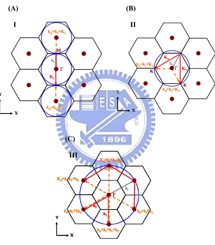
[18, 19]Figure 2.4(A) shows a band diagram of a triangular-lattice photonic crystal. The points I, II, and III are the points Γ1, M1, and K1, respectively. The reciprocal space of the structure is a
space combined by hexagons. Figure 2.4(B) shows a schematic diagram of a reciprocal space. The K1 and K2 are the Bragg vectors with the same magnitude, |K|=2π/a, where a is the lattice
constant of the photonic crystal. Consider the TE modes in the 2-D photonic crystal structure, the diffracted light wave from the structure must satisfy the relationship:
... , 2 , 1 , 0 q , K q K q k kd = i + 1 1 + 2 2 1,2 = ± ± i d =ω ω
where kd is xy-component wave vector of diffracted light wave, ki is xy-component wave
vector of incident light wave, q1,2 is order of coupling, ωd is the frequency of diffracted light
wave, and ωi is the frequency of incident light wave.
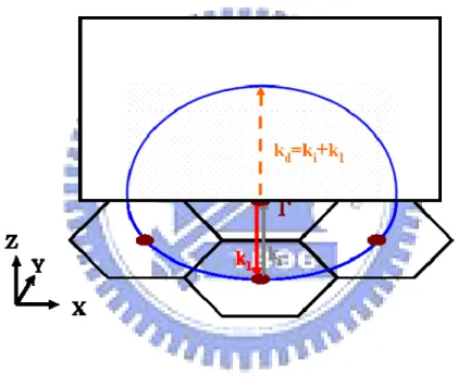
It is expected lasing occurs at specific points on the Brillouin-zone boundary (Γ, M, and K) and at the points at which bands cross and split. At these lasing points, waves propagating in different directions couple to significantly increase the mode density. It is particularly interesting that each of these points exhibits a different type of wave coupling. For example, as shown in figure 2.5(A), the coupling at point I only involves two waves, propagating in the forward and backward directions. This coupling is similar to that of a conventional DFB laser. However, there can be six equivalent Γ-M directions in the structure; that is, the cavity can exist independently in each of the three different directions to form three independent lasers. Point II has a unique coupling characteristic unachievable in conventional DFB lasers, the coupling of waves propagating in three different directions as shown in figure 2.5(B). This (2.22) (2.21)
means the cavity is a triangular. In fact, there can also be six Γ-K directions in the structure;
therefore, two different lasing cavities in different Γ-K directions coexist independently. At point III the coupling includes waves in in-plane all six directions; 0°, 60°, 120°, -60°, -120°, and 180° as shown in figure 2.5(C). In addition, the coupled light can be emitted perpendicular from the surface according to first order Bragg diffraction, as shown in figure 2.6. This is the same phenomenon that occurs in conventional grating-coupled surface-emitting lasers.