國
立
交
通
大
學
電機學院 電子與光電學程
碩
士
論
文
射頻橫向擴散金氧半場效電晶體之基
體電壓及熱載子效應研究
Bulk Bias and Hot Carrier Effects in RF
LDMOS
研 究 生:牟宗文
指導教授:郭浩中 教授
陳坤明 教授
射頻橫向擴散金氧半場效電晶體之基體電壓及熱載子效應研究
Bulk Bias and Hot Carrier Effects in RF LDMOS
研 究 生:牟宗文 Student:Zong-Wen Mou
指導教授:郭浩中 陳坤明 Advisors:Hao-Chung. Kuo 陳坤明 Kun Ming Chen
國 立 交 通 大 學
電機學院 電子與光電學程
碩 士 論 文
A Thesis
Submitted to College of Electrical and Computer Engineering National Chiao Tung University
in partial Fulfillment of the Requirements for the Degree of
Master of Science in
Electronics and Electro-Optical Engineering Sep. 2010
Hsinchu, Taiwan, Republic of China
射頻橫向擴散金氧半場效電晶體之基體電壓及熱載
子效應研究
學生 牟宗文 指導教授 : 郭浩中 教授 陳坤明 博士國立交通大學 電機學院 電子與光電學程碩士班
摘 要
橫向擴散金氧半場效電晶體(LDMOS)已被廣泛應用於無線基地台的應用,因為其優 越的性能,成本,可靠度和功率。一個技術的挑戰,是如何在導通電阻和崩潰電壓作權 衡。為了克服這一障礙,一個新的環形結構在本論文中提出。比傳統結構擁有較低導通 電阻,同時可保持相同的崩潰電壓。隨著電路設計的用途和可靠度的問題逐漸重視,這 篇論文也探討對兩者結構基體電壓和熱載子效應的特性。 我們實驗裡使用的 電晶體 是用聯電 0.5 微米LDMOS的製程製作的。我們分別針對傳 統和環形結構在各種基體電壓跟熱載子驅迫下進行了直流跟射頻的分析。結果發現,環 形結構因減少了導通電阻而抑制了準飽和效應的發生。不過,環形結構的截止頻率和最 大振盪頻率卻較傳統結構為低。當外加基體電壓時,我們發現兩種結構,在中低的電流 範圍射頻性確能改善。然而,進入高電流範圍射頻性能卻開始退化。此外,傳統結構對 直流和射頻參數的變比環形更為敏感。在第四章中,我們進一步研究LDMOS的熱載子效 應。結果發現,該元件的導通電阻容易因驅迫而退化。對於高頻參數的退化上,我們發 現有個異常現象,傳統結構在增加熱載子驅迫下反而提高最高振盪頻率。此外,我們也 發現,環形結構由於有較大的碰撞游離在熱載子驅迫下退化的比傳統結構更嚴重。從以上的觀察,我們認為雖然環形結構具有較好的直流性能,但其射頻性能可能變得更糟。 另外,環形結構對基體電壓的敏感性和熱載子驅破的免疫力也是較差的。
Bulk Bias and Hot Carrier Effects in RF
LDMOS
Student: Zong Wen Mou Advisors: Dr. Hao-Chung Kuo
Dr. Kun-Ming Chen
Degree Program of Electrical and Computer Engineering
National Chiao Tung University
ABSTRACT
Lateral-diffused metal-oxide-semiconductor field-effect transistor (LDMOS) has been widely used in wireless base-station application due to its advantages in performance, cost, reliability, and power capability. A challenge to the LDMOS technology is the trade-off between the on-resistance and breakdown voltage. To overcome this obstacle, a new “Ring” structure has been presented in this thesis. Lower on-resistance is achieved as compared to the conventional “Finger” structure while keeping the same breakdown voltage. With the purposes of circuit design and reliability issue, the bulk bias and hot carrier effects on the performances of LDMOS with different layout structures are also investigated in this thesis.
The transistors used in our work were fabricated with the UMC 0.5 μm LDMOS process.
The DC and RF characteristics of the LDMOS with “Finger” and “Ring” layouts were analyzed under various bulk biases and hot carrier stress times. Our results show that the quasi-saturation effect is suppressed in the “Ring” structure due to reduced on-resistance. However, the cutoff frequency and maximum oscillation frequency of the “Ring” structure are lower than that of the “Finger” one. When a reverse bulk voltage is applied, we found that the RF performances are improved in the low and medium current ranges for both layout
structures. However, the RF performance is degraded in high current range. In addition, the changes of the DC and RF parameters in the “Finger” structure are more sensitive to the bulk voltage than that in the “Ring” one. In chapter4, we further study the hot carrier effects on the performances of LDMOS. It is shown that the most degrading parameter is on-resistance. For the degradations of the high-frequency parameters, an abnormal phenomenon is observed in “Finger” device, that is, the maximum oscillation frequency is increased after hot carrier stress. Moreover, we found that the performances of the “Ring” structure under hot carrier stress are degraded more seriously than that of the “Finger” one, owing to the larger impact ionization. From above observations, we concluded that although the “Ring” structure has better DC performance than the “Finger” one, its RF performance may become worse. In addition, the bulk bias sensitivity and the hot carrier immunity of the “Ring” device are also lower than that of the “Finger” device.
誌 謝
這篇論文能完成,首先要感謝指導教授的細心及耐心的指導; 再來要感謝
所有國家奈米元件實驗室的朋友們,在我實驗上提供的幫助; 最後要謝謝我
的妻子不論發生什麼事總是在身後默默的支持我.謝謝你們!!
Content
Chinese Abstract
………
i
English Abstract
………
ii
………
Acknowledgements
iii
Content
………
iv
Figure Caption
………
v
Chapter 1
Introduction
1.1 Introduction to RF LDMOS………
1
1.2 Motivation………
2
1.3 Thesis Organization………
3
Chapter 2
Characteristics of RF LDMOS
2.1 Introduction………
4
2.2 Device Structure………
4
2.3 Principle of Operation………
5
2.4 DC Characteristics………
5
2.5 Small-Signal Characteristics………
6
2.6 RF Power Characteristics………
7
2.7 Conclusion………
8
Chapter 3
Bulk Bias Effect
3.1 Introduction………
18
3.2 DC Performance………
18
3.3 RF Performance………
19
3.4 Model Analysis………
20
3.5 Comparison of “Finger” and “Ring” Structures………
22
3.6 Conclusion………
23
Chapter 4
Hot Carrier Effect
4.1 Introduction………
38
4.2 Hot Carrier Effect on DC Performance………
39
4.3 Hot Carrier Effect on RF performance………
41
4.4 Conclusion………
42
Chapter 5
Conclusion………
53
Reference
……… 55
Figure Caption
Chapter 2
Fig. 2.1 LDMOS layout structures: (a) Finger and (b) Ring 09 Fig. 2.2 Schematic cross-section of the RF LDMOS transistor 10 Fig. 2.3 ID-VG characteristics of the LDMOS with different layout structures at (a)
VD=0.1V and (b) VD=12V 11 Fig. 2.4 ID-VD characteristics of the LDMOS with different layout structures 12 Fig. 2.5 (a) Ac current gain H21 and (b) maximum available gain as
functiofrequency 13 Fig. 2.6 (a) Cutoff frequency and (b) maximum oscillation frequency as functions of gate
voltages for LDMOS with different layout structures… 14 Fig. 2.7 Small-signal equivalent circuit of an RF LDMOS 15 Fig. 2.8 Output power, power gain and PAE versus input power in an RF LDMOS with
“Finger” structure 16 Fig. 2.9 Output power and IM3 versus input power in an RF LDMOS with “Finger” structure 17
Chapter 3
Fig. 3.1 Schematic cross-section of the RF LDMOS transistor without butting
contact 24 Fig. 3.2 ID-VG characteristics of the LDMOS with “Finger” structure at (a) VD=0.1V and
(b) VD=12V 25 Fig. 3.3. (a) Cutoff frequency and (b) maximum oscillation frequency as functions of gate
voltages for LDMOS with different bulk voltages 26 Fig. 3.4. (a) Cutoff frequency and (b) maximum oscillation frequency as functions of the
Fig. 3.5. (a) Cutoff frequency and (b) maximum oscillation frequency as functions of drain current for LDMOS with different bulk voltages 28 Fig. 3.6 Relationship of power gain with the drain current at different bulk voltages for the
“Finger” structure. The measurement frequency is 1.8 GHz 29 Fig. 3.7. (a) Cutoff frequency and (b) maximum oscillation frequency change percentage
with each model parameter 30 Fig. 3.8. Relationship of the measured transconductance and the cutoff frequency with the
drain current at different bulk voltages 31 Fig. 3.9. Relationship of the gate capacitance (Cgs+Cgd) and the cutoff frequency with the
drain current at different bulk voltage 32 Fig. 3.10 Relationship of the total resistance (Rg+Rd+Rs) and the maximum oscillation
frequency with the drain current at different bulk voltages 33 Fig. 3.11 (a) Cutoff frequency and (b) maximum oscillation frequency as functions of the gate
overdrive voltage for LDMOS with different bulk voltages and layout
structures 34 Fig. 3.12 (a) Cutoff frequency and (b) maximum oscillation frequency as functions of drain
current for LDMOS with different bulk voltages and layout
structures. 35 Fig. 3.13 The relationship of the measured transconductance with the drain current at
different bulk voltages and layout structures 36 Fig. 3.14 Relationship of the measured gate-source capacitance with the drain current at
different bulk voltages and layout structures 37
Chapter 4
Fig. 4.1 ID-VG characteristics of the LDMOS before and after hot carrier stresses at (a) VD=0.1V and (b) VD=12V 43
Fig. 4.2 ID-VD characteristics of the LDMOS under hot carrier stress 44 Fig. 4.3 Threshold voltage shifts of the LDMOS with “Finger” and “Ring” structures under
hot carrier stress. The stressing voltage is VG=2.5V and VD=26V
and (b) VD=28 V 45 Fig. 4.4 Transconductance degradations of the LDMOS with “Finger” and “Ring” structures
under hot carrier stress. The stressing voltage is VG=2.5V and (a) VD=26V and (b) VD=28 V 46 Fig. 4.5 Saturation current degradations of the LDMOS with “Finger” and “Ring” structures
under hot carrier stress. The stressing voltage is VG=2.5V and (a) VD=26V and (b) VD=28 V … 47 Fig. 4.6 On-resistance degradations of the LDMOS with “Finger” and “Ring” structures
under hot carrier stress. The stressing voltage is VG=2.5V and (a) VD=26V and (b) VD=28 V 48 Fig. 4.7 Bulk current of the LDMOS with “Finger” and “Ring” structures at
VD=26V 49 Fig. 4.8 Impact ionization efficiency of the LDMOS with “Finger” and “Ring” structures at
VD=26V 50 Fig. 4.9 (a) Cutoff frequency and (b) maximum oscillation frequency as functions of gate
voltages before and after hot carrier stress 51 Fig. 4.10 (a) Cutoff frequency and (b) maximum oscillation frequency degradations under
hot carrier stress at VG=2.5V and VD=26V in the “Finger” and “Ring”
Chapter 1
Introduction
1.1 Introduction to RF LDMOS
Nowadays, the power devices play an important role of the recent electronics industry. One of them is silicon lateral diffused metal oxide semiconductor field effect transistor (LDMOS), which has played a dominant role in wireless base-station application for high frequency range up to 2 GHz the last ten years, due to its advantages in performance, cost, reliability, and power capability [1-6].
Owing to some advantages of LDMOS, it has been used in high power and high frequency applications. Because the source and p-body terminals of the LDMOS connect to each other and then pull-up to ground, the source inductance can be reduced, and thus the power gain can be improved dramatically. In the past, the most popular high-speed device is bipolar transistor for power amplifier applications. But their collector terminal requires insulating from the ground and the emitter terminal needs to connect to the ground. So a longer metal line has to be drawn than that of LDMOS, which will increase the inductance and reduce their power gain. Moreover, the LDMOS is a lateral structure device, which has lower feedback capacitance compared with a bipolar transistor. Therefore, the LDMOS provides higher gain than bipolar device for the same output power level. Besides, the LDMOS has better linear relationship between the drain current and gate voltage, which can improve their linearity. Also, the LDMOS can sustain higher drain voltage because of their lateral diffusion structure, which makes the device stronger in reliability. Finally, the LDMOS has mature IC-technology like CMOS and is fabricated on the silicon substrate to reduce the cost. Above all, we know the LDMOS has higher power gain, linearity, reliability, and lower
1.2 Motivation
With process technology development, the device will be smaller by reducing channel length. And LDMOS also scales down the channel length and the drift length to reduce on-resistance and increase transconductance. However, there is a challenge in scaling down due to high-voltage on working. One of the solutions to solve the trade-off between the on-resistance and breakdown voltage is optimizing the layout design. The “Ring” structure has been designed to reduce the on-resistance, but keep the same breakdown voltage. In this thesis, two types of layout structures (“Finger” and “Ring”) have been studied for DC and high-frequency characteristics.
In recent years, digital radio-frequency personal communication devices such as cellular telephones, cordless telephones, PBX, and LAN, utilizing the band between 900 MHz and 2.5 GHz, have played an increasingly important role in the overall wireless communication infrastructure. The major challenge in these devices is to design bulk silicon LDMOS technology, which is compatible with CMOS and passive components, for the implementation of RF integrated power amplifiers (IPA’s) used in portable wireless communication
applications [7]. In these integrated circuits, the source and bulk terminals of LDMOS may
not be connected together and biased at different voltages. For this reason, it is interesting to know the variations of the device characteristics as the bulk voltage has been changed. Besides, making the bulk bias to be controlled individually might improve the RF performance and enable new applications [8]. In the thesis, we investigate the DC and RF performances of LDMOS with different bulk biases by breaking the butting contact between the source and bulk terminals.
When an LDMOS transistor is operated under pinch-off condition, also known as “saturated case”, hot carriers traveling with saturation velocity can cause parasitic effects at the drain side of the channel known as “hot carrier effects” (HCE). The hot-carrier effect in
high-voltage LDMOS has been noticed on DC characterization recently [9-15]. However, the high-frequency performance of LDMOS under hot carrier stress is seldom addressed. H. Xiao et al studied the hot carrier effects on the RF performance of the LDMOS with a novel structure in drift region, which was fabricated with standard 0.18 µm CMOS technology [16]. A. Mai et al improved the RF LDMOS reliability by optimizing the doping profile in the drift region [17]. However, the hot carrier instability in different device layout structures is still not discussed. In this thesis, the hot carrier effects on both the DC and high-frequency characteristics of LDMOS with the “Ring” and “Finger” structures are studied. In addition, we extracted the small-signal model parameters with stressing time to explain the degradation of RF performance.
1.3 Thesis Organization
The content in this thesis includes the following parts.
Chapter 1 introduces the LDMOS for RF applications and the motivation of this thesis. Chapter 2 compares the DC and high frequency performances of LDMOS with different layout structure. In addition, the small-signal model parameters were extracted to investigate their effects on the cutoff frequency and maximum oscillation frequency.
In Chapter 3, the DC, high frequency and RF power performances of LDMOS with bulk bias are analyzed. Also, the small-signal model parameters were extracted to explain the behaviors of cutoff frequency and maximum oscillation frequency with the change of bulk bias.
Chapter 4 presents the hot carrier effects on the DC and high frequency performances of LDMOS. To find the mechanism of the high-frequency performance degradation under hot carrier stress, the small-signal model parameters are analyzed.
Chapter 2
Characteristics of RF LDMOS
2.1 Introduction
In high-power applications, the RF transistors are usually implemented in a “Finger” structure, as shown in Fig. 2.1(a). For RF performance concern, multi-finger layouts are used to design wide MOSFETs for reducing the gate resistance. Since the gate resistance would limit the power gain attainable at some frequencies. The drain resistance is the main component in LDMOS to have influence on the on-resistance (Ron). Here, in order to achieve lower Ron, we adopted a “Ring” structure, which is different from the “Finger” one in the LDMOS layout design, as shown in Fig. 2.1(b). In this chapter, we will describe the DC and RF characteristics of RF LDMOS with different layout structures.
2.2 Device Structure
RF LDMOS transistors were fabricated using the UMC 0.5 µm 40V LDMOS process.
The schematic cross section of the device is shown in Fig. 2.2. The drift region was extended under the field oxide and consisted of a lightly doped N-well and an N- region with higher doses for on-resistance control. The source region and the p-body were tied together to eliminate extra surface bond wires to reduce the source inductance and improve the RF performance in a power amplifier configuration. The gate oxide thickness was 135 Å and the
channel length (Lg) was 1.2 µm. The “Finger” structure used in this study had 2 or 10 cells
which each cell had 4 gate fingers with finger width Lf =10 µm. For the “Ring” structures, the
width of each gate ring was 40m and each cell was arranged as a 1x2 or 5x2 array in one
device. The drain region surrounded the source region, while the gate was located between the source and the drain, as shown in Fig. 2.1 (a).
2.3 Principle of Operation
The operation of the RF LDMOS is similar to the general MOSFET. Their difference is
that we use the N- region to replace the heavy doping of the N+ region, to increase the
sustained drain voltage. Because the N
-When we add the gate voltage, the electrons below their gate oxide form an inversion layer, and then we add drain terminal voltage to force the electrons flow into the drain terminal to yield the current. Because their light dope of the N- region we will get a larger turn-on resistance (Ron) than the general MOSFET.
region can consume most voltage drop coming from drain terminal, a higher avalanche breakdown can be achieved. The gate voltage is limited by their thickness of the gate oxide.
2.4 DC Characteristics
The LDMOS devices studied in our work have the following feature: gate oxide
thickness tox =135 Å, field oxide thickness tFOX
Figure 2.4 compares the output characteristics of LDMOS with different layouts. The
=3000 Å, channel length Lg =1.2 µm, and
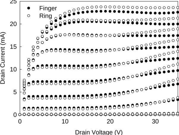
total device width W=80 µm. The ID-VG characteristics of the LDMOS with different layout structures are shown in Fig.2.3. The threshold voltages (VT) of “Finger” and “Ring” structures are 0.86 and 0.88 V, respectively. The slight different VT between these two devices might be due to the different p-body thermal diffusion and suggests that the “Ring” device has a higher channel doping concentration than the “Finger” one. In linear region (VD=0.1V), the “Ring” and “Finger” structures have similar transconductance, whereas, in saturation region (VD =12V), the “Ring” device shows a higher transconductance at high gate voltages. Because the “Finger” structure has larger effective drain resistance, which reduces the drain current, the average current density is lower than that in “Ring” one.
been observed at sufficiently high gate voltages, where a unique phenomenon in LDMOS called “quasi-saturation effect” happens. This effect limits the maximum drain current at high gate voltages. It is because of the existence of the light doping drift region. The drain current tends to be saturated not because of the pinch-off of the channel at the drain terminal, rather because of the velocity saturation in the drift region, which like as JFET or series a nonlinear resistance controlled by drain current. We extracted the on-resistance of the “Finger” and “Ring” structures, and their values are 123 and 111 ohm, respectively, indicating the “Finger” one has higher drain resistance. Therefore, a larger voltage drop in drift region will exist in “Finger” device, making the carriers in the drift region will enter the velocity saturation earlier than that in “Ring” structure. In other words, the “Finger” structure has more serious “quasi-saturation effect” than that in “Ring” one.
2.5 Small-Signal Characteristics
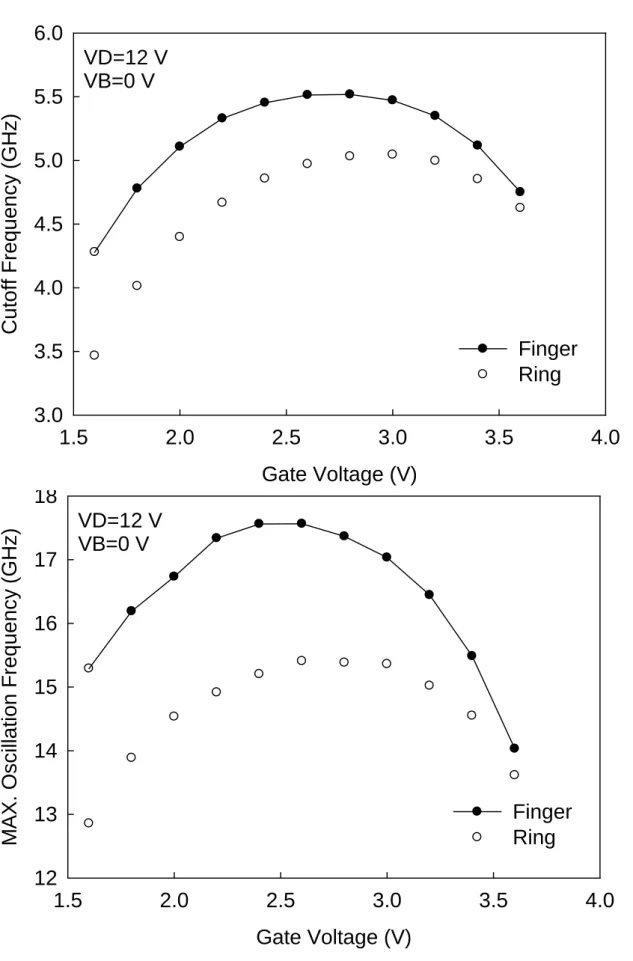
To characterize the RF performance of the LDMOS, the S-parameters must been measured. We set the frequency from 100MHz to 20 GHz using an HP8510 network analyzer and then de-embedded by subtracting the OPEN dummy. Then we get the hybrid parameter (H21) and unilateral power gain, which were calculated by the S-parameter, as shown in Fig.
2.5. From Fig. 2.5(a), we extracted the cutoff frequency (FT) by the intersection of the
frequency, in which the hybrid parameter (H21) is zero dB, as indicated by the red arrowed point. Similarly, we can extract the maximum oscillation frequency (Fmax) from Fig. 2.5(b). The measured the cutoff frequency and Fmax are shown in Fig. 2.6. The RF LDMOS were measured at drain voltage VD=12 V with different gate voltages. As observed in Fig. 2.6, the cutoff frequency had maximum values at gate voltage VG=3V, where the transconductance has a maximum value. With increasing the gate voltage, both the cutoff frequency and the maximum oscillation frequency decreased because of the mobility degradation and quasi-saturation effects. In addition, the “Finger” structure has larger the cutoff frequency and
the maximum oscillation frequency at the same gate voltage than that in “Ring” structure.
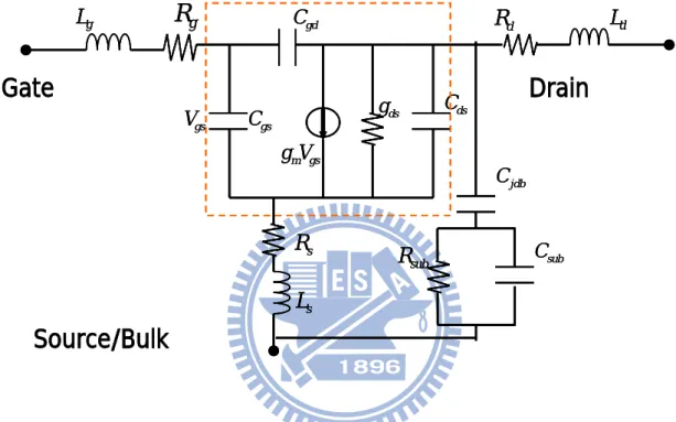
By analyzing the small-signal equivalent circuit of the RF LDMOS, as shown in Fig. 2.7,
we can extract the model parameters based on curve-fitting method proposed by S. C. Wang [18]. The extracted model parameters are listed in Table 2.1 at VD=12V and VG=3V.
Table 2.1 Small-signal model parameters for “Finger” and “Ring” structures.
Gm(mA/V) Cgs(fF) Cgd(fF) Rs(Ω) Rg(Ω) Rd(Ω) Csub(fF) Rsub(kΩ) Cjdb(fF)
Finger 7.40 197 18.2 1.14 15.5 25.5 1.10 2.69 17.5
Ring 7.37 203 19.9 1.09 14.4 20.1 1.51 2.66 18.9
We know the cutoff frequency and the maximum oscillation frequency can be
expressed respectively as [19] gg m T g C f ∝ / , (1) and gd gd gs m s d g ds T C C C g R R R g f f + + + + ≈ π 2 ) ( * max . (2)
According to Table 2.1, we find that the higher cutoff frequency in the “Finger” structure is mainly due to the higher transconductance compared to that in “Ring” one. The
transconductance difference will make a 1.6 % FT difference, as shown in Fig. 2.6. But the
difference of the maximum oscillation frequency between the “Finger” and “Ring” is larger than that in the cutoff frequency. Maybe the increased gate resistance further reduces the maximum oscillation frequency in the “Ring” structure.
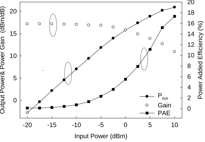
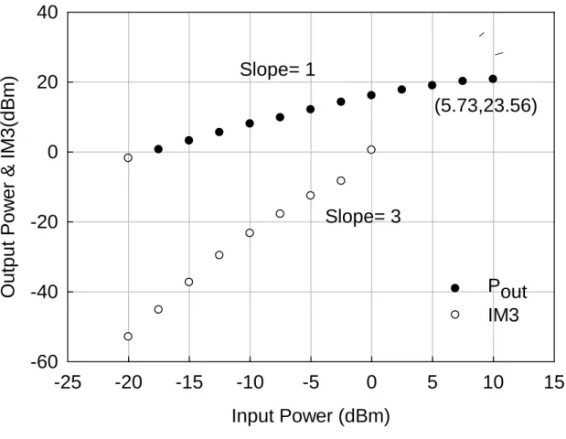
RF power characterization was performed using the load-pull measurement. The source and load impedances were tuned for maximum power gain and maximum output power, respectively. The measured output power, power gain and power-added efficiency (PAE) of an RF LDMOS are shown in Fig. 2.8. The gate bias is VG =3.2V and the drain bias is VD =12V at 1.8 GHz. The linear power gain is about 17 dB. At high input powers, the gain will be compressed. The main reason for gain compression is attributed to the clipping effect [20].
The output power at 1-dB compression point (Pout, 1dB
To characterize the linearity, the third-order intercept point, at which the output power and third-order intermodulation (IM3) are equal, is commonly used. For low distortion operation, the third-order intercept point should be as high as possible. Figure 2.9 shows the output power and IM3 versus input power of the RF LDMOS with “Finger” structure. We extended the output power and IM3 curves with straight lines of slope 1 and 3, individually, to obtain a third-order intercept point (IP3). As shown in the Fig. 2.9, the input and output
third-order intercept points (IIP3 and OIP3) are 5.73 and 23.56 dBm, respectively.
) is 15.2 dBm. In addition, the maximum PAE is 17.3%.
2.7 Conclusion
LDMOS with different structures for RF applications are investigated. The “Ring” structure has smaller on-resistance than that in “Finger” structure. Besides, the quasi-saturation effect is suppressed in the RF LDMOS with the ring structure. However, the
cutoff frequency of the “Ring” is reduced due to lower transconductance. Finally, we show
Fig. 2.3 ID-VG characteristics of the LDMOS with different layout structures at (a) VD=0.1V and (b) VD=12V. Gate Voltage (V) 1 2 3 4 D rai n C ur rent ( A ) 10-9 10-8 10-7 10-6 10-5 10-4 10-3 10-2 10-1 T ransco nduct ance ( m A /V ) 0.0 2.0 4.0 6.0 8.0 Finger Ring VD=12 V Gate Voltage (V) 0 1 2 3 4 D rai n C ur rent ( A ) 10-10 10-9 10-8 10-7 10-6 10-5 10-4 10-3 T ransco nduct ance ( m A /V ) 0.0 0.1 0.2 0.3 0.4 0.5 0.6 0.7 Finger Ring VD=0.1 V
Fig. 2.4 ID-VD characteristics of the LDMOS with different layout structures
Drain Voltage (V)
0
10
20
30
D
rai
n C
ur
rent
(
m
A
)
0
5
10
15
20
25
Finger
Ring
Frequency (Hz)
10
810
910
10U
ni
lat
er
al
P
ow
er
G
ai
n
(dB
)
-20
-10
0
10
20
30
40
50
VG=1.6 V
VG=1.8 V
VG=2.0 V
VG=2.2 V
VG=2.4 V
VG=2.6 V
VG=2.8 V
VG=3.0 V
VG=3.2 V
VG=3.4 V
Frequency (Hz)
10
810
910
10U
ni
lat
er
al
P
ow
er
G
ai
n
(dB
)
-20
-10
0
10
20
30
40
50
VG=1.6 V
VG=1.8 V
VG=2.0 V
VG=2.2 V
VG=2.4 V
VG=2.6 V
VG=2.8 V
VG=3.0 V
VG=3.2 V
VG=3.4 V
Frequency (Hz) 108 109 1010 M agni tude of H 21( dB ) 0.1 1 10 100 VG=1.6 V VG=1.8 V VG=2.0 V VG=2.2 V VG=2.4 V VG=2.6 V VG=2.8 V VG=3.0 V VG=3.2 V VG=3.4 V Frequency (Hz) 108 109 1010 M agni tude of H 21( dB ) 0.1 1 10 100 VG=1.6 V VG=1.8 V VG=2.0 V VG=2.2 V VG=2.4 V VG=2.6 V VG=2.8 V VG=3.0 V VG=3.2 V VG=3.4 VFig. 2.6 (a) Cutoff frequency and (b) maximum oscillation frequency as functions of gate voltages for LDMOS with different layout structures.
Gate Voltage (V)
1.5
2.0
2.5
3.0
3.5
4.0
M
A
X
. O
scilla
tio
n
F
re
q
u
e
n
cy
(
G
Hz)
12
13
14
15
16
17
18
Finger
Ring
VD=12 V
VB=0 V
Gate Voltage (V)
1.5
2.0
2.5
3.0
3.5
4.0
C
ut
of
f F
requency
(
G
H
z)
3.0
3.5
4.0
4.5
5.0
5.5
6.0
Finger
Ring
VD=12 V
VB=0 V
Fig. 2.7 Small-signal equivalent circuit of an RF LDMOS. gd C gs C Cds s R g
R
d R g L Ld s L ds g gs mV g gs V jdb C sub C sub RGate
Drain
Source/Bulk
gd C gs C Cds s R gR
d R g L Ld s L ds g gs mV g gs V jdb C sub C sub RGate
Drain
Source/Bulk
Fig. 2.8 Output power, power gain and PAE versus input power in an RF LDMOS with “Finger” structure.
Input Power (dBm)
-20
-15
-10
-5
0
5
10
O
ut
put
P
ow
er
&
P
ow
er
G
ai
n (
dB
m
/dB
)
0
5
10
15
20
P
ow
er
A
dded E
ff
ici
ency
(
%
)
0
2
4
6
8
10
12
14
16
18
20
P
outGain
PAE
Fig. 2.9 Output power and IM3 versus input power in an RF LDMOS with “Finger” structure.
Input Power (dBm)
-25
-20
-15
-10
-5
0
5
10
15
O
ut
put
P
ow
er
&
I
M
3(
dB
m
)
-60
-40
-20
0
20
40
Pout
IM3
Slope= 1
Slope= 3
(5.73,23.56)
Chapter 3
Bulk Bias Effect
3.1 Introduction
In modern circuit applications, the bulk voltage is not always common and different bulk voltages will change the device characteristics. Therefore, it is important to investigate the bulk bias effect in RF LDMOS. In this chapter, the butting contact in source and p-body terminals is broken, as shown in Fig. 3.1. Different bulk voltages are supplied to study the changes of DC and RF parameters. Firstly, we study the characteristics of the “Finger” structure with different bulk biases. Then we compare the different bulk bias effects on the
“Finger” and “Ring” structures. From the measured S-parameters, we extracted the model
parameters in small-signal equivalent circuit to interpret the bulk-voltage dependences of the
cutoff frequency (FT) and the maximum oscillation frequency (Fmax
). Finally, we show the RF power performance of the RF LDMOS with different bulk voltages.
3.2 DC Performance
The RF LDMOS devices studied in our work have the following feature: gate oxide
thickness tox =135 Å, field oxide thickness tFOX =3000 Å, channel length Lg =1.2 µm, and
device width W =400 µm. The ID-VG characteristics of the RF LDMOS with different bulk voltages are shown in Fig. 3.2. In linear operation (VD =0.1V), the threshold voltage (VT) changes from 0.93 V to 2.20 V as the bulk voltage (VB) changes from 0 to -4 V. Since the bulk voltage influences the threshold voltage, it can be thought of as a second gate, and is sometimes referred to as the "Back-Gate"; the body effect is sometimes called the "Back-Gate Effect". First, because the added bulk voltage reduces the gate voltage control and thus a larger gate voltage is needed to turn-on the transistor, a larger threshold voltage will be
achieved. Second, the maximum transconductance of the device with VB=-4 V is lower than that with VB=0 V, because of the reduced mobility coming from the pull-down of the back gate. When the devices operate in saturation region (VD=12 V), similar maximum transconductances are observed with different bulk voltages, but the VB-induced gate voltage shift is same as that in linear region.
3.3 RF Performance
The high-frequency characteristics of the RF LDMOS transistors are shown in Fig. 3.3. The devices were measured at drain voltage VD=12 V with different gate voltages and
different bulk voltages. As observed in Fig. 3.3, when the VB is 0 V, both the cutoff
frequency and maximum oscillation frequency have maximum values at gate voltage VG=2.8 V, where the transconductance has a maximum value. With the bulk voltage increases, the peak of the transconductance moves from VG =2.8 V to VG =3.8 V, both the cutoff frequency and maximum oscillation frequency move either. But the maximum values of both the cutoff frequency and maximum oscillation frequency are independent of the bulk voltage, which are about 4.5 and 17 GHz, respectively. Keep on increasing the gate voltage, both the cutoff frequency and maximum oscillation frequency decrease because of the mobility degradation and quasi-saturation effect. With higher bulk voltages, the cutoff frequency and maximum oscillation frequency drop more steeply. In other word, the mobility degradation and quasi-saturation effect become worse with increasing the bulk voltage.
The “Body Effect” describes the changes in the threshold voltage by the change in the bulk voltage. So we remove the influence of the threshold voltage from gate voltage (gate overdrive voltage; VG-VT), as shown in Fig. 3.4. It shows the relationship of the measured
cutoff frequency and maximum oscillation frequency with the gate overdrive voltage at
the cutoff frequency and maximum oscillation frequency are 3.4% and 3.1%, respectively, when the VB changes from 0 V to -4 V. However, the trend is reverse when the gate overdrive voltage increases above 1.4V because of
For RF circuit design, the power transistor is usually biased at a constant current source.
the mobility degradation and quasi-saturation effect.
So we are interested to see the cutoff frequency and maximum oscillation frequency as functions of the drain current, as shown in Fig. 3.5. In the low and medium current range (ID<40 mA), the cutoff frequency and maximum oscillation frequency raise with increasing bulk voltage. It indicates that the added bulk bias can improve the high-frequency performance. The maximum gain
The relationship of the measured power gain with the drain current at different bulk voltages for the “Finger” structure is shown in Fig. 3.6. The gain is stayed in the stable state in zero bulk bias. Since increasing the bulk bias increases the cutoff frequency, the power gain is increased. However, the power gain is reduced at high currents due to the decrease of cutoff frequency.
is about 3.7% for VB change from 0 V to -4V at the same drain current.
3.4 Model Analysis
To demonstrate the dependences of the cutoff frequency and maximum oscillation frequency with bulk bias, we extracted the parameters in a small-signal equivalent circuit model [21]. Using extracted parameters from the existing device and altering one parameter at the time, the effect of model parameters on the cutoff frequency and maximum oscillation frequency can be visualized. The influences of model parameters on the cutoff frequency and maximum oscillation frequency are shown in Fig. 3.7. The x-axis showed the parameter value departures from the initial value in percent. The y-axis showed the change in frequency in percent. As shown in Fig. 3.6(a), both the transconductance (Gm) and the gate-source capacitance (Cgs) have major impact on the cutoff frequency, but the gate-drain capacitance
(Cgd) has minor impact on the cutoff frequency.
According to above description, we focus the influence of both the extracted transconductance and the gate-source capacitance on the cutoff frequency. Fig. 3.8 shows the relationship of the extracted transconductance and the extracted cutoff frequency
Since the maximum oscillation frequency is related to the cutoff frequency strongly, both the transconductance and the gate-source capacitance have influence on the maximum oscillation frequency. In addition to the above extracted model parameters, we also extracted the drain resistance (Rd), the gate resistance (Rg), the source resistance (Rs), the bulk resistance (Rsub), the bulk capacitance (Csub), and the drain-bulk junction capacitance (Cjdb). They are the composition of maximum oscillation frequency. As shown in Fig. 3.7(b), both the gate resistance and the drain resistance have major impact on the maximum oscillation frequency; the others have less impact on the maximum oscillation frequency.
The gate-source capacitances with different bulk voltages are shown in Fig. 3.9. The separation of the gate-source capacitance due to the change of bulk voltage gradually becomes larger with increasing drain current. At low and medium currents (ID <40 mA), the change of gate capacitances with bulk voltage is small, so the change of cutoff frequency is mainly due to the transconductance. When the drain current increases beyond 40 mA, the change of gate with the
drain current at different bulk voltages. The cutoff frequency should be proportional to the
transconductance. With increasing the bulk voltage, the transconductance is increased and thus the cutoff frequency is also increased. At ID= 30mA, a maximum difference is observed between VB=0 V and -4 V, where the changes of transconductance and cutoff frequency are 3.6% and 3.7%, respectively. Therefore, the transconductance has domain influence on the cutoff frequency. When the drain current goes higher than 40mA, the cutoff frequency reduces with increasing VB. Since the transconductance is still increased with VB in this region, the influence of the gate-source capacitances must also be considered.
voltage at high currents.
Finally, we research the influence of the resistance at different bulk voltages, as shown in Fig. 3.10. The total resistance (Rd+Rg+Rs) increases with increasing drain current. However, it is slightly changed by the bulk voltage. So the total resistance (Rd+Rg+Rs) is not the domain variable in the maximum oscillation frequency when varying the bulk voltage. Consequently, the change of maximum oscillation frequency with bulk voltage is mainly attributed to the change of cutoff frequency.
3.5 Comparison of “Finger” and “Ring” Structures
Next, we compare the bulk voltage effect on the characteristics of LDMOS with different layout structures. Their cutoff frequency and maximum oscillation frequency as functions of gate overdrive voltage (VG-VT) at different bulk voltage are shown in Fig. 3.11. As can be seen, the changes of the cutoff frequency and maximum oscillation frequency in the “Finger” structure with the change of bulk voltage are larger than that in the “Ring” one. For example, at VG-VT=1.3 V, the change of cutoff frequency in the “Finger” structure is 3.4%, while that in the “Ring” structure is only 1.5%. It indicates that the high-frequency performance of the “Finger” structure is more sensitive to the bulk voltage than that of the “Ring” one.
The cutoff frequency and maximum oscillation frequency as functions of the drain current with different layout structures and bulk voltages are shown in Fig. 3.12. Similar to the results in Fig. 3.11, larger changes of cutoff frequency and maximum oscillation frequency in the “Finger” structure than that in “Ring” one with the change of bulk voltage are also observed. At ID=20~30 mA, the change of cutoff frequency in “Finger” structure is 2.3% while that in the “Ring” structure is only
Fig. 3.13. shows the relationship of the measured transconductance with the drain current at different bulk voltages and layout structures.
0.3%.
the transconductance between VB=0 and -4 V in the “Finger” structure is larger than that in the “Ring” one. In the current range of 20~30 mA, the change of transconductance in the “Finger” structure is 3.3%, while that in the “Ring” structure is 0.6%.
Fig. 3.14 shows the relationship of the measured gate-source capacitances with the drain current at different bulk voltages and layout structures.
So the less change of the cutoff frequency and maximum oscillation frequency in “Ring” structure is due to the less change of transconductance. Since the transconductance is not the only factor affecting the cutoff frequency, we should also observe the influence of the gate-source capacitances in the two different layout structures.
When the current is below 30mA, the measured gate-source capacitances are nearly unchanged by bulk bias for these two devices. Above 30mA, the change of the measured gate-source capacitances between VB=0 and -4 V is enlarged. According to the above statement in the low and medium current range,
the transconductance is a dominant factor in the change of cutoff frequency and maximum
oscillation frequency with bulk bias, while, in the high current range, the influence of gate-source capacitance will become large.
3.6 Conclusion
LDMOS with different bulk biases for RF applications were investigated. The RF performances were improved by increasing bulk bias. In the low and medium current range,
the increase of the transconductance is the main factor for the RF performance improvement.
However, the RF performance is degraded in high current range due to the influence of the gate-source capacitance. Finally, we found that the high-frequency performance of the “Finger” structure is more sensitive to the bulk voltage than that of the “Ring” one.
Fig. 3.2 ID-VG characteristics of the LDMOS with “Finger” structure at (a) VD=0.1V and (b)
Gate Voltage (V)
0
1
2
3
4
D
rai
n C
ur
rent
(A
)
10
-1010
-910
-810
-710
-610
-510
-410
-310
-210
-1T
ransco
nduct
ance
G
m
(
m
A
/V
)
0
10
20
30
40
VB=0 V
VB=-4 V
Finger
VD=12 V
Gate Voltage (V) 0 1 2 3 4 5 D rai n C ur rent ( A ) 10-13 10-12 10-11 10-10 10-9 10-8 10-7 10-6 10-5 10-4 10-3 10-2 T ransco nduct ance ( m A /V ) 0.0 0.5 1.0 1.5 2.0 2.5 3.0 3.5 VB=0 V VB=-4 V Finger VD=0.1 VFig. 3.3. (a) Cutoff frequency and (b) maximum oscillation frequency as functions of gate voltages for LDMOS with different bulk voltages.
Gate Voltage (V)
1.5
2.0
2.5
3.0
3.5
4.0
4.5
5.0
M
A
X
. O
scilla
tio
n
F
re
q
u
e
n
cy
(
G
Hz)
11
12
13
14
15
16
17
18
VB=0 V
VB=-2 V
VB=-4 V
Finger
VD=12 V
Gate Voltage (V)
1.5
2.0
2.5
3.0
3.5
4.0
4.5
5.0
C
ut
of
f F
requency
(
G
H
z)
3.2
3.4
3.6
3.8
4.0
4.2
4.4
4.6
VB=0 V
VB=-2 V
VB=-4 V
Finger
VD=12 V
Fig. 3.4. (a) Cutoff frequency and (b) maximum oscillation frequency as functions of the gate
Gate Overdrive Voltage (V)
0.0
0.5
1.0
1.5
2.0
2.5
3.0
M
A
X
. O
scilla
tio
n
F
re
q
u
e
n
cy
(
G
Hz)
10
11
12
13
14
15
16
17
18
VB=0 V
VB=-2 V
VB=-4 V
Finger
VD=12 V
Gate Overdrive Voltage (V)
0.0
0.5
1.0
1.5
2.0
2.5
3.0
C
ut
of
f F
requency
(
G
H
z)
3.2
3.4
3.6
3.8
4.0
4.2
4.4
4.6
VB=0 V
VB=-2 V
VB=-4 V
Finger
VD=12 V
Fig. 3.5. (a) Cutoff frequency and (b) maximum oscillation frequency as functions of drain current for LDMOS with different bulk voltages.
Drain Current (mA)
0
10
20
30
40
50
60
70
80
M
A
X
. O
scilla
tio
n
F
re
q
u
e
n
cy
(
G
Hz)
10
11
12
13
14
15
16
17
18
VB=0 V
VB=-2 V
VB=-4 V
Finger
VD=12 V
Drain Current (mA)
0
10
20
30
40
50
60
70
80
C
ut
of
f F
requency
(
G
H
z)
3.2
3.4
3.6
3.8
4.0
4.2
4.4
4.6
VB=0 V
VB=-2 V
VB=-4 V
Finger
VD=12 V
Fig. 3.6 Relationship of power gain with the drain current at different bulk voltages for the “Finger” structure. The measurement frequency is 1.8 GHz.
Drain Current (mA)
0
10
20
30
40
50
60
70
80
G
ai
n (
dB
)
14
15
16
17
18
19
20
VB=0 V
VB=-4 V
Fig. 3.7. (a) Cutoff frequency and (b) maximum oscillation frequency change percentage with each model parameter.
Parameter Change Percentage (%)
-40
-30
-20
-10
0
10
20
30
40
M
A
X
. O
sci
llat
ion F
requency
C
hange P
er
ce
nt
age (
%
)
-8
-6
-4
-2
0
2
4
6
8
10
Rd
Rg
Rs
Cjdb
Csub
Rsub
Parameter Change Percentage (%)
-40 -30 -20 -10 0 10 20 30 40 M A X . O s c ill at ion F req uenc y C hang e P er c ent ag e (% ) -30 -20 -10 0 10 20 30 Gm Cgd Cgs
Fig. 3.8. Relationship of the measured transconductance and the cutoff frequency with the drain current at different bulk voltages.
Drain Current (mA)
0
10
20
30
40
50
60
70
T
ransco
nduct
ance
(
A
/V
)
22
24
26
28
30
32
34
36
38
40
C
ut
of
f F
requency
(
G
H
z)
3.2
3.4
3.6
3.8
4.0
4.2
4.4
4.6
VB=0 V
VB=-4 V
Finger
Fig. 3.9. Relationship of the gate capacitance (Cgs+Cgd) and the cutoff frequency with the drain current at different bulk voltages.
Drain Current (mA)
10
20
30
40
50
60
C
gs
+
C
gd (
pF
)
0.9
1.0
1.1
1.2
1.3
1.4
1.5
1.6
C
ut
of
f F
requency
(
G
H
z)
3.2
3.4
3.6
3.8
4.0
4.2
4.4
4.6
VB=0 V
VB=-4 V
Finger
Fig. 3.10 Relationship of the total resistance (Rg+Rd+Rs) and the maximum oscillation frequency with the drain current at different bulk voltages.
Drain Current (mA)
20
30
40
50
60
70
Rg
+
Rd
+
Rs(
o
h
m
)
7.5
8.0
8.5
9.0
9.5
10.0
10.5
M
A
X
. O
scilla
tio
n
F
re
q
u
e
n
cy
(
G
Hz)
10
11
12
13
14
15
16
17
18
VB=0
VB=-4
Fig. 3.11 (a) Cutoff frequency and (b) maximum oscillation frequency as functions of the gate overdrive voltage for LDMOS with different bulk voltages and layout structures.
Gate Overdrive Voltage (V)
0.0
0.5
1.0
1.5
2.0
2.5
3.0
M
A
X
. O
scilla
tio
n
F
re
q
u
e
n
cy
(
G
Hz)
10
12
14
16
18
VB=0 V
VB=-4 V
VB=0 V
VB=-4 V
Circle : Ring
Triangle : Finger
Gate Overdrive Voltage (V)
0.0
0.5
1.0
1.5
2.0
2.5
3.0
C
ut
of
f F
requency
(
G
H
z)
2.0
2.5
3.0
3.5
4.0
4.5
VB=0 V
VB=-4 V
VB=0 V
VB=-4 V
Circle : Ring
Triangle : Finger
Fig. 3.12 (a) Cutoff frequency and (b) maximum oscillation frequency as functions of drain current for LDMOS with different bulk voltages and layout structures.
Drain Current (mA)
0
10
20
30
40
50
60
70
M
A
X
. O
scilla
tio
n
F
re
q
u
e
n
cy
(
G
Hz)
8
10
12
14
16
18
VB=0 V
VB=-4 V
VB=0 V
VB=-4 V
Circle : Ring
Triangle : Finger
Drain Current (mA)
0
10
20
30
40
50
60
70
C
ut
of
f F
requency
(
G
H
z)
1.5
2.0
2.5
3.0
3.5
4.0
4.5
5.0
VB=0 V
VB=-4 V
VB=0 V
VB=-4 V
Circle : Ring
Triangle : Finger
Fig. 3.13 Relationship of the measured transconductance with the drain current at different bulk voltages and layout structures.
Drain Current (mA)
0
10
20
30
40
50
60
70
T
ransco
nduct
ance
(
A
/V
)
10
15
20
25
30
35
40
VB=0 V
VB=-4 V
VB=0 V
VB=-4 V
Circle : Ring
Triangle : Finger
Fig. 3.14 Relationship of the measured gate-source capacitance with the drain current at different bulk voltages and layout structures.
Drain Current (mA)
0
20
40
60
80
C
gs(pF
)
0.8
0.9
1.0
1.1
1.2
1.3
1.4
VB=0 V
VB=-4 V
VB=0 V
VB=-4 V
Circle : Ring
Triangle : Finger
Chapter 4
Hot Carrier Effect
4.1 Introduction
When an LDMOS transistor is operated under pinch-off condition, also known as “saturated case”, hot carriers traveling with saturation velocity can cause parasitic effects at the drain side of the channel known as “hot carrier effects” (HCE). These carriers have sufficient energy to generate electron-hole pairs by impact ionization. The generated minority carriers can either be collected by the drain or injected into the gate oxide. The generated majority carriers create a bulk current which can be used as a measurable quantity to determine the level of impact ionization.
Carrier injection into the gate oxide can lead to hot carrier degradation effects such as threshold voltage changes due to occupied traps in the oxide. Hot carriers can also generate traps at the silicon-oxide interface known as “fast surface states” leading to sub-threshold swing deterioration and stress-induced drain leakage. In general, these degradation effects set a limit to the lifetime of a transistor; therefore they have to be controlled as well as possible. The presence of such injected carriers in the oxides triggers numerous physical damage processes that can drastically change the device characteristics over prolonged periods. The accumulation of damage can eventually cause the circuit to fail as key parameters shift. The useful lifetime of integrated circuits based on the LDMOS devices are thus affected by the lifetime of the LDMOS device itself. So, the hot carrier degradation in the LDMOS must be well understood.
In this chapter, an investigation of the hot-carrier degradation in the high voltage LDMOS transistors with different structures is presented. The degradations of DC and RF performances under hot carrier stress are observed in these devices. From the measured
S-parameters, we extracted the model parameters in a small-signal equivalent circuit to determine the mechanism of the RF performance degradation.
4.2 Hot Carrier Effect on DC Performance
The hot carrier effects on the ID-VG characteristics of an LDMOS are shown in Fig. 4.1. The stressing time is 3 hr. The threshold voltage (VT) is not changed a lot after hot carrier stress, whereas, the transconductance is degraded. In linear region (VD=0.1 V), the transconductance degradation is mainly attributed to the mobility degradation. When the device operates in saturation region (VD=12 V), the transconductance degradation is serious at high gate voltages due to the enhanced quasi-saturation effect under hot carrier stress.
Figure 4.2 compares the output characteristics of LDMOS before and after hot carrier stresses. The gate voltages are biased at 0 ~ 5 V. It is observed that the stressed device has more serious “quasi-saturation effect” than the fresh one. After extracting the on-resistance of these devices, we find that the on-resistance will be degraded 12% under hot carrier stress, indicating the drain resistance of the stressed device is increased due to damage. Therefore, a larger voltage drop in drift region will exist after hot carrier stress, making the carriers in the drift region will enter the velocity saturation earlier than that before hot carrier stress.
Figure 4.3 compares the threshold voltage shift of the LDMOS with “Finger” and “Ring” structures under hot carrier stress. For stressing voltage VD=26V. Similar threshold voltage shift is observed for these two devices. However, when the stressing voltage is increased to 28V, a larger threshold voltage shift is observed in the “Ring” structure than that in the “Finger” structure. Fig. 4.4 shows the transconductance degradation of the LDMOS with “Finger” and “Ring” structures. At 26V stressing voltage, the transconductances in the “Finger” and “Ring” structures have similar changes, whereas, at stressing voltage VD=28V, the transconductance degradation in the “Ring” structure becomes larger than that in the
as shown in Fig. 4.5.
Figure 4.6 shows the on-resistance degradation of the LDMOS with the “Finger” and “Ring” structures under hot carrier stress. The degradations in the “Ring” structure are larger than that in the “Finger” structure for both stressing voltages VD=26 V and 28 V. The difference is more apparent at higher stressing voltage. Comparing Figs 4.3 – 4.6, we find that the degradation of on-resistance is more serious than the degradations of other parameters. Such a result suggests that the stress-induced oxide damage in the drift region is larger than that in the channel region, because the change of on-resistance comes from the increased oxide/Si interfacial traps in the drift region [22].
Based on the above observations, we know that the DC performance of the “Ring”
structure under hot carrier stress is degraded more seriously than that of the “Finger” one.We
compare the bulk current in the “Finger” and “Ring” structures and find that the “Ring” device has larger maximum value than the “Finger” one. Since the “Ring” structure has lower drift resistance, the voltage drop in the drift region is lower that of “Finger” structure. Therefore, a higher electric field may exist in the drain side of the intrinsic device, and more electron-hole pairs would be generated. As a result, the “Ring” structure has higher bulk
current than that of the “Finger” one [23]. In addition, we compare the impact ionization
efficiency of the LDMOS with “Finger” and “Ring” structures under hot carrier stress. As shown in Fig. 4.8, the maximum impact ionization efficiency in the “Ring” is larger than that in the “Finger” one, suggesting that the “Ring” structure has a higher lateral electric field and a more serious impact ionization [24]. Therefore, the “Ring” structure will suffer more damage than the “Finger” one under hot carrier stress, leading to larger dc degradations.
4.3 Hot Carrier Effect on RF performance
The high-frequency characteristics of the RF LDMOS transistors with “Finger” structure under stress voltage VD=26 V are shown in Fig. 4.9. The devices were measured at drain
voltage VD=12 V with different gate voltages. After hot carrier stress, the maximum value of the cutoff frequency is slightly degraded (~ -0.65%), whereas, that of the maximum oscillation frequency is increased (~ +3.3%). Keep on increasing the gate voltage, both the cutoff frequency and maximum oscillation frequency decrease after stress due to the mobility degradation and the quasi-saturation effect becomes worse.
According to the extracted model parameters listed in Table 4.1, we know that the slight
degradation in FT is probably due to the reduction of gate-to-drain capacitance (Cgd) after
stress, which weakens the influence of the Gm degradation. Since the Cgd has large impact on
the Fmax (see eq. (2) of Chapter 2), the reduction of Cgd even results in the enhancement of
the Fmax after stress.
Table 4.1 Small-signal model parameters of the “Finger” device before and after stress. Gm (mA/V) Cgs (fF) Cgd (fF) Rs (Ω) Rg (Ω) Rd (Ω) Csub (fF) Rsub (kΩ) Cjdb (fF) Before stress 6.86 181 17.9 1.14 22.3 25.6 1.02 3.61 15.4 After stress 6.64 180 14.7 1.14 22.3 27.7 0.87 3.99 14.7
Then we compare the degradations of the high-frequency characteristics in different layout structures shown in Fig. 4.10. The stress condition is VG=2.5V and VD=26V. As
shown in Fig. 4.10(a), the FT degradation in the “Ring” structure is larger than that in the
“Finger” one. After 10800 s stress, the FT degradations in the ”Finger” and “Ring” structures
are 0.65% and 2.32%, respectively. For Fmax degradation, an abnormal phenomenon has been
observed. In Fig. 4.10(b), we find that the Fmax is reduced for both devices under hot carrier
stress before 200 s, and the degradation of the “Ring” structure is higher than that of the
increasing stress time, but the Fmax in “Ring” structure is still decreased. After 10800 s stress,
the changes of the Fmax in the ”Finger” and “Ring” structures are +3.26% and -0.96%,
respectively. Owing to the large Gm degradation in “Ring” structure, the reduction of Cgd
after stress cannot cancel the influence of Gm degradation. Eventually,the increase of Fmax
induced by hot carrier stress is not occurred in the “Ring” structure.
4.4 Conclusion
The hot carrier effects on the DC and RF performances of the LDMOS transistors with
different structures are presented in this chapter. Our results show that the transconductance degradation is larger at high gate voltages than that at low and medium gate voltages due to the enhanced quasi-saturation effect under hot carrier stress. Besides, we find that the degradation of on-resistance is more serious than the degradations of other DC parameters due to larger oxide damage in the drift region than that in the channel region. After hot carrier stress, the maximum oscillation frequency of the “Finger” structure is increased due to the reduced Cgd. Finally, it is found that the performances of the “Ring” structure under hot carrier stress are degraded more seriously than that of the “Finger” one. So we deduce that the “Finger” structure has higher hot carrier immunity than the “Ring” one.
Fig. 4.1 ID-VG characteristics of the LDMOS before and after hot carrier stresses at (a) VD=0.1V and (b) VD=12V.
Gate Voltage (V)
0
1
2
3
4
5
D
rai
n C
ur
rent
(
A
)
10
-910
-810
-710
-610
-510
-410
-310
-210
-1 T rans c onduc tanc e G m (m A /V )0.0
2.0
4.0
6.0
8.0
Fresh
Stressed
VD=12 V
Gate Voltage (V)
0
1
2
3
4
5
D
rai
n C
ur
rent
(
A
)
10
-1010
-910
-810
-710
-610
-510
-410
-3 T rans c onduc tanc e G m (m A /V )0.0
0.1
0.2
0.3
0.4
0.5
0.6
0.7
Fresh
Stressed
VD=0.1 V
Fig. 4.2 ID-VD characteristics of the LDMOS under hot carrier stress.
Drain Voltage (V)
0
10
20
30
D
rai
n C
ur
rent
(
m
A
)
0
5
10
15
20
25
Fresh
Stressed
Fig. 4.3 Threshold voltage shifts of the LDMOS with “Finger” and “Ring” structures under
Stressing Time (s)
10
110
210
310
410
5T
hr
esh
ol
d V
ol
tage S
hi
ft
(
m
V
)
10
-110
010
110
2Finger
Ring
Stressing Time (s)
10
110
210
310
410
5T
hr
esh
ol
d V
ol
tage S
hi
ft
(
m
V
)
10
-110
010
110
2Finger
Ring
Fig. 4.4 Transconductance degradations of the LDMOS with “Finger” and “Ring” structures under hot carrier stress. The stressing voltage is VG=2.5V and (a) VD=26V and (b) VD=28 V.
Stressing Time (s)
10
110
210
310
410
5T
ransco
nduct
ance
D
egr
adat
ion (
%
)
10
-110
010
110
2Finger
Ring
Stressing Time (s)
10
110
210
310
410
5T
ransco
nduct
ance
D
egr
adat
ion (
%
)
10
-110
010
110
2Finger
Ring
Fig. 4.5 Saturation current degradations of the LDMOS with “Finger” and “Ring” structures under hot carrier stress. The stressing voltage is VG=2.5V and (a) VD=26V and (b) VD=28 V.
Stressing Time (s)
10
110
210
310
410
5S
at
ur
at
ion C
ur
rent
D
egr
adat
ion (
%
)
10
010
110
2Finger
Ring
Stressing Time (s)
10
110
210
310
410
5S
at
ur
at
ion C
ur
rent
D
egr
adat
ion (
%
)
10
010
110
2Finger
Ring
Fig. 4.6 On-resistance degradations of the LDMOS with “Finger” and “Ring” structures under hot carrier stress. The stressing voltage is VG=2.5V and (a) VD=26V and (b) VD=28 V.
Stressing Time (s)
10
110
210
310
410
5O
n-R
esi
st
ance
D
egr
adat
ion (
%
)
10
010
110
2Finger
Ring
Stressing Time (s)
10
110
210
310
410
5O
n-R
esi
st
ance
D
egr
adat
ion(
%
)
10
010
110
2Finger
Ring
Fig. 4.7 Bulk current of the LDMOS with “Finger” and “Ring” structures at VD=26V.
Gate Voltage (V)
0
2
4
6
8
10
12
B
u
lk
C
u
rre
n
t (mA
)
0.0
0.2
0.4
0.6
0.8
1.0
1.2
1.4
1.6
1.8
Finger
Ring
Fig. 4.8 Impact ionization efficiency of the LDMOS with “Finger” and “Ring” structures at VD=26V.