國 立 交 通 大 學
電子工程學系 電子研究所碩士班
碩 士 論 文
奈米級蕭特基金氧半場效電晶體之載子傳輸特性
與通道背向散射研究
The Carrier Transport and Channel Backscattering
Characteristics of Nanoscale Schottky-Barrier MOSFETs
研 究 生: 鄧安舜
指導教授: 莊紹勳 博士
奈米級蕭特基金氧半場效電晶體之載子傳輸特性
與通道背向散射研究
The Carrier Transport and Channel Backscattering
Characteristics of Nanoscale Schottky-Barrier MOSFETs
研 究 生 : 鄧安舜 Student : An-Shun Teng
指導教授 : 莊紹勳 博士 Advisor : Dr. Steve S. Chung
國立交通大學
電子工程學系 電子研究所碩士班
碩士論文
A Thesis
Submitted to Department of Electronics Engineering & Institute of
Electronics College of Electrical Engineering and Computer Science
National Chiao Tung University
in Partial Fulfillment of the Requirements
for the Degree of Master of Science
in Electronics Engineering
August 2009
Hsinchu, Taiwan, Republic of China.
中華民國 九十八 年 八 月
奈米級蕭特基金氧半場效電晶體之載子傳輸特性與
通道背向散射研究
學生:鄧安舜 指導教授:莊紹勳 博士
國立交通大學 電子工程學系 電子研究所碩士班
摘要
在前瞻超大型積體電路元件中,為了提升元件的效能,許多新穎的元件結構已被廣 泛的提出,例如:高介電係數介電層、應變矽通道、金屬閘極與金屬源/汲極結構。當元 件微縮至奈米級尺寸時,通道背向散射理論已經成功的運用在預測元件微縮極限上。而 今,由於蕭特基金氧半場效電晶體製作的最佳化方法已趨可行,其在前瞻元件演進的地 位已大幅的提升。因此,蕭特基金氧半場效電晶體的載子傳輸特性的研究成為主要課題。本論文中,我們首先著眼於利用活化能(Activation Energy Method)方法求得等效的蕭 特基位障勢。蕭特基場效電晶體之汲極電流傳導機制與閘極電壓的關係式可利用等效蕭 特基位障勢表示。另外,我們同時發現蕭特基金氧半場效電晶體在打開狀態時,產生一 個負等效蕭特基位障勢,使通道背向散射原理可運用於此。以往,溫度相依法(Temperature Dependent Method)常被用來探討通道背向散射係數。但是,在蕭特基金氧半場效電晶體 中,載子主要是透過熱場發射機制由源極入射制通道內。所以對此元件來說,溫度相依 法是不可行的。為了要求得載子彈道入射的機率,我們導入了等效彈道遷移率(Effective Ballistic Mobility)的觀念,此原理是建立在載子遷移率(Mobility)會隨著通道縮小而下降 的因素上。因此,我們可以透過等效彈道遷移率的方法得到載子在元件線性區的彈道入 射係數與載子熱入射(Thermal Injection Velocity)速度。然後,我們運用當電晶體在負等
效蕭特基位障勢發生時的載子平均傳輸速度(Carrier Average Velocity)與載子熱入射速度 上,藉由這兩個速度的關係式,載子在打開狀態時的載子彈道入射機率即可求得。 由本文的研究,我們得到幾個結論: (1) 背向散射理論在蕭特基金氧半場效電機體 中,因負等效位障勢的產生而再度的適用, (2) 載子由源極經通道到達汲極的背向散射 機率因非局部的熱場穿遂機制而較傳統金氧半場效電晶體高, (3) 應變矽通道元件對背 向散射係數影響較輕,但對載子熱入射速度影響較劇烈, (4) 遷移擴散(Drift-Diffusion) 模型在quasi-ballistic區仍適用。因此,蕭特基金氧半場效電晶體加上高參雜隔離層(Dopant Segregation Implantation)與CESL(Contact-Etched Stoped Layer)技術,可達道元件高速操作 的需求。
The Carrier Transport and Channel Backscattering
Characteristics of Nanoscale Schottky-Barrier MOSFETs
Student:An-Shun Teng
Advisor:Dr. Steve S. Chung
Department of Electrical Engineering & Institute of Electronics
National Chiao Tung University
Abstract
In advanced VLSI devices, a lot of new structures have been brought up for enhancing drain current such as strained-Si channel, high-κ dielectric, metal gate and metal source/drain. In the nanoscale channel length, the channel backscattering theory has been applied to predict the scaling-limitations of these structures successfully. Nowadays, the Schottky-barrier MOSFETs have aroused much more attention because some optimized processes become feasible. Hence, the carrier transport mechanism of Schottky-barrier MOSFETs from source to drain becomes the most popular topic in researches.
In the thesis, first, we will focus on finding the effective Schottky-barrier height from the activation energy method. We can describe the effective Schottky-barrier height versus carrier transport mechanism relationship from this method. A negative effective Schottky-barrier height is found in the ON-state of the Schottky-barrier MOSFETs so that the channel backscattering theory can be used for extracting the carrier ballistic rate. In the past, the ballistic coefficient is extracted by temperature dependent method. However, the major carrier transport mechanism in the Schottky-barrier MOSFET is field emission, the
from mobility degradation in short channel devices. We may directly obtain the ballistic coefficient and thermal injection velocity in the linear region. Then, we derive the carrier average velocity versus thermal injection velocity relations in ON-state. By the two velocity components, the ballistic probability of the Schottky-barrier MOSFET can be extracted easily.
Based on the results of this work, it was concluded that: (1) the backscattering theory is practicable from the negatively effective Schottky-barrier height, (2) the backscattering probability in the source side of Schottky-barrier is smaller than that in the conventional MOSFETs due to non-local tunneling, (3) the strained technology affects the backscattering coefficient lightly but it affects the thermal injection velocity drastically, (4) the drift-diffusion model is still workable in quasi-ballistic region. Thus, Schottky-barrier MOSFET with dopant segregation implantation and CESL(Contact-Etched Stoped Layer) can enhance the ballistic rate and thermal injection velocity that produced high speed operation in Schottky-barrier MOSFETs.
Acknowledgments
研究所生涯雖短,但經歷了這兩年的學習過程後,相信對於往後無論在生活、職場 與待人處事上均有深遠的影響。首先,我把這份誠摯的感謝獻給陪伴著我兩年的研究生 活,並一直是我的良師兼益友,且在國內外均享譽盛名的 莊紹勳教授,感謝您在這數 百個研究日子裡,對我的諄諄教誨。 感謝博士班的易叡學長,教導我實驗室的各種規範,並給予我實驗上的實質幫助, 預祝您往後的研究能突飛猛進。感謝已經畢業的學長們,家銘、小郭、有良跟文彥,除 了在修課上的幫助外,感謝您們在實驗技巧與研究方向上的提點。感謝汪大暉教授門下 的學長與同學們,小馬、達達、佑亮、阿標跟阿杜,對於實驗碰到的奇奇怪怪的問題, 多虧有您們豐富的學識與經驗幫我一一克服。感謝一路陪伴我完成實驗的同學,振鵬, 感謝您在實驗上的執著,讓我在實驗系統與實驗方法上,有更深入的了解與認識。感謝 健宏,感謝您敏銳的心思,讓我在各項事務上均能盡善盡美。感謝米華,這位實驗室的 精神領袖,使實驗室的氣氛活絡。感謝學弟們,士嵩、政穎、永涵跟元宏,感謝你們在 我的研究與生活中的許多照應,並和我一起分擔辛勞。感謝同為前瞻元件與技術實驗室 的各位,讓這個大家庭充滿歡笑與喜悅。另外還要感謝提供元件的聯華電子與在各期刊 論文中給予我智慧的古聖先賢。 最後也是最值得感謝的就是我的家人們。感謝爺爺奶奶對我成長過程中無微不至的 照顧,感謝爸爸媽媽對我在學生生涯中最完整的學習規劃,感謝姊姊一直擔任我學習的 榜樣,讓我有今天的成就。 謹將這份榮耀獻給我的家人們。Contents
Chinese Abstract iii
English Abstract v
Acknowledgements vii
Contents viii
Figure Captions x
Table Captions xiv
Chapter 1 Introduction 1
1.1 Motivation 1
1.2 Organization of Thesis 2
Chapter 2 Overview of Metal S/D Schottky-Barrier MOSFETs 4
2.1 Metal-Semiconductor Junctions 4
2.1.2 Energy Band Diagram 4
2.1.2 Effective of the Fermi Level Pinning 5
2.1.3 Image-Force Lowering 6
2.2 Current transport Mechanism in Metal-Semiconductor Diode 6
2.2.1 Thermoionic Emission Current 7
2.2.2 Field Emission Current 7
2.2.3 Measurement of the Schottky-Barrier Height 8 2.3 Introduction of the Schottky-Barrier MOSFET 9
2.4 TheOperational Principle 10
2.5 The Challenges and New Technologies of SBMOS 11 2.5.1 Reduction of Schottky-Barrier Height 11
2.5.2 Modern Technologies for SB-CMOS 12
Chapter 3 Device Preparation and Basic Characteristics 24
3.1 Devices Preparation 24
3.2 Measuring Facility and Basic Experimental Setup 25 3.3 Basic Characteristics of the Schottky-Barrier MOSFETs 26
3.3.1 Band Diagram of DSI-SBMOS 26
3.3.2 Basic Characteristics of DSI-SBMOS 27
3.5 Summary 30
Chapter 4 Carrier Ballistic Transport in Schottky-Barrier MOSFETs 48
4.1 Introduction of Ballistic Theory 48
4.1.1 To Derive the Backscattering Theory 49
4.1.2 Temperature Dependent Method to Extract Backscattering
Coefficient 52 4.2 Characteristics of the Backscattering Theory 53 4.2.1 The Drain and Gate Voltage Dependences 54 4.2.2 The Mobility versus Drain Current Relationship 55 4.3 Backscattering Theory in Schottky-Barrier MOSFETs 56
4.3.1 Effective Ballistic Mobility 57
4.3.2 The Links Between Ballistic Theory, Effective Ballistic
Mobility and Drift-Diffusion Model 58
4.4 The Experimental Results of Effective Ballistic Mobility 60
4.5 Summary 62
Chapter 5 Backscattering Coefficient in the Velocity Saturation Region 73
5.1 Thermal Injection Velocity 73
5.2 Carrier Average Velocity in the Saturation Region 75 5.3 The Experimental Results of the Velocity Components 77
5.4 Summary 79
Chapter 6 Conclusions 91
Figure Captions
Fig. 2.1 Energy band diagram of a Schottky contact (a) under non-equilibrium condition and (b) equilibrium condition.
Fig. 2.2 Energy band diagram of a Schottky contact (a) without and (b) with the effect of surface states. The Fermi level is pushed to 0.
Fig. 2.3 Image force induced Schottky-barrier lowering.
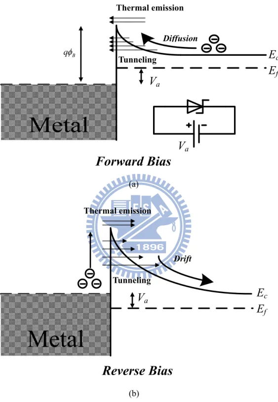
Fig. 2.4 Carrier transport mechanism of the Schottky contact in N-type semiconductor. (a) under forward bias (b) under reverse bias.
Fig. 2.5 Band diagram to deduce the probability of field emission (a) light doped condition (b) heavy doped (degenerate) condition (c) under reverse bias condition of a junction between n-type semiconductor and metal.
Fig. 2.6 Extracting the Schottky-barrier height by activation-energy method.
Fig. 2.7 The device structures (a) conventional MOSFET (b) Schottky- barrier MOSFET. Fig. 2.8 Different band diagram of n-SBMOSFET (SB-NMOS). (a) OFF-state, Vg<Vfb (b)
OFF-state, Vg=Vfb (c) Vg>Vfb.
Fig. 2.9 Current components in the source to channel interface of Schottky-barrier nMOSFETs.
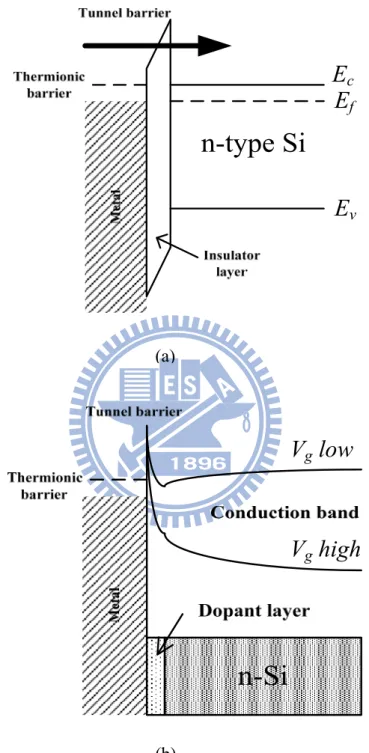
Fig. 2.10 Schottky barrier height reduction technology (a) with insulator layer (b) with dopant segregation implantation.
Fig. 2.11 Drivability of Schottky barrier MOSFET as a function of Schottky barrier height for (a) N-type and (b) P-type devices.
Fig. 3.1 Process flow of Schottky-barrier MOSFETs with DSI NiPt silicide. Fig. 3.2 (a) Device split of Schottky-barrier MOSFETs with DSI NiPt silicide and
conventional MSOFET and (b) its cross-section TEM picture with the shortest length 35nm.
Fig. 3.3 (a) The Ion-Ioff characteristics of Sample A, B and C. Sample B has the optimized
Fig. 3.5 Conduction band diagram of the (a) conventional SBMOS (b) SBMOS with dopant segregation implantation (DSI-SBMOS) when VD is small bias.
Fig. 3.6 Short channel effect of the DSI-SBMOS.
Fig. 3.7 Some characteristics of the DSI-SBMOS (a) ID-VG curve (b) ID-VD curve.
Fig. 3.8 Drain current versus gate voltage curve (ID-VG) with different DSI energy when
|VD|=0.1V. (a) SB-PMOS (b) SB-NMOS.
Fig. 3.9 The effective Schottky-barrier height of different DSI energy in SB-PMOS.
Fig. 3.10 The conduction band edge of SBMOS with different bias condition. The dashed line is OFF-state and solid line is ON-state.
Fig. 3.11 The effective Schottky-barrier height of SB-PMOS with different bulk bias (VB).
Fig. 3.12 The band diagram for different substrate bias of (a) VB=0 (b) VB<0 for
Schottky-barrier pMOSFETs.
Fig. 3.13 The effective Schottky-barrier height of both N and PMOS with different channel length.
Fig. 3.14 The conduction band edge with different devices (a) Conventional SBMOS (b) DSI-SBMOS (c) Conventional MOSFET. The solid line is short channel and dash line is long channel devices.
Fig. 3.15 The band diagram of the DSI-SBMOS with different DSI energy in (a) ON-state (b) OFF-state. The DSI energy of the blue line is lower than red line. The dash line is the conventional SBMOS band diagram.
Fig. 4.1 (a) Band diagram of the conventional NMOS with the scattering matrix method for extracting the ballistic theory. (b) The simplified transmission and reflection current flow.
Fig. 4.2 The conduction band edge versus position with several bias condition (a) VD=50mV,
VG=0~0.6V (b) VD=0.6V, VG=0~0.6V (c) VG=50mV, VD=0~0.6V (d) VG=0.6V,
VD=0~0.6V.
Fig. 4.3 The reflection coefficient versus gate voltage plot with different drain voltage. Circle is at V =0.1V, square is at V =0.5V and triangle is at V =1V.
Fig. 4.4 The band diagram for (a) DSI-SBMOS (b) concentional MOSFETs with the same channel length and potential. υinj means the injection velocity.
Fig. 4.5 (a) The scattering components in the channel. (b) Drift velocity versus electric field plot. Solid line is experiment curve, dash line is theoretical curve. υs is saturation
velocity, and εc is critical field.
Fig. 4.6 The low field mobility versus channel length plot (a) for DSI SB-PMOS with CESL (b) Conventional pMOSFET.
Fig. 4.7 The low field mobility versus channel length plot (a) for DSI SB-NMOS with CESL (b) Conventional nMOSFET.
Fig. 4.8 The linear ballistic coefficient (Blin) versus channel length curve (a) for DSI
SB-PMOS with CESL (b) DSI SB-NMOS with CESL compared with conventional MOSFETs.
Fig. 4.9 The thermal injection velocity in linear region of (a) SB-PMOS versus PMOS (b) SB-NMOS versus NMMOS.
Fig. 5.1 (a) Equilibrium thermal injection velocity versus inversion layer density ns and also
shown the Fermi velocity [33]. (b) Electron charge Qi(0) at the top of the barrier versus VDS.
Fig. 5.2 The potential profiles from source toward drain (a) Conventional MOSFETs with doped S/D (b) Schottky-barrier MOSFETs.
Fig. 5.3 The carrier average velocity (effective velocity) of (a) Schottky-barrier pMOSFETs. (b) Conventional pMOSFETs with doped S/D.
Fig. 5.4 The carrier average velocity (effective velocity) of (a) Schottky-barrier nMOSFETs. (b) Conventional nMOSFETs with doped S/D.
Fig. 5.5 Comparison of the carrier average velocity (effective velocity) between (a) PMOS and SB-PMOS (b) NMOS and SB-NMOS.
Fig. 5.6 Comparison of the effective saturation velocity between (a) PMOS and SB-PMOS (b) NMOS and SB-NMOS.
temperature between (a) PMOS and SB-PMOS (b) NMOS and SB-NMOS. Fig. 5.8 The inversion charge density of the Schottky-barrier MOSFET with DSI. Fig. 5.9 The electric field of the channel potential (a) DSI SB-PMOS and conventional
PMOS (b) DSI SB-NMOS and conventional NMOS.
Fig. 5.10 The saturation ballistic coefficient (Bsat) of (a) DSI SB-PMOS and conventional
PMOS (b) DSI SB-NMOS and conventional NMOS.
Fig. 5.11 The current enhancement rate of uniaxial tensile-cap compared to conventional structure.
Table Captions
Tab. 3.1 Splits of SBMOS with different DSI energies. The DSI energy relation is DSI1 <
Chapter 1
Introduction
1.1 Motivation
Modern VLSI devices have entered nanoscale era for several years and continue to be scaled rapidly. By ITRS predictions, semiconductor industry will meet the scaling-limit in ten or less years. In order to understand the limitations of down-scaling, some researchers have investigated these device bahariors by the ballistic transport theory, such as M. Lundstrom
[1-6] and M. J. Chen [7-8].
When the channel length is just a few nanometers, some transport carriers can easily emit through the channel without any collisions. As the length scales down, more carriers are easier to tunneling through the channel barrier. Hence, the drift-diffusion theory has less significant for increasing tunneling rate. Before the channel is short enough for all transport carriers to tunnel through, we call it “quasi-ballistic” region. In this region, we have two important parameters which includes backscattering coefficient (rc) and thermal injection velocity ( ). T The former presents the carrier transmission rate in the channel barrier and the other means the limitation of carrier transport velocity. By the two parameters, we can describe how close to the limit of the devices.
In recent years, ballistic transport has investigated in various devices such as process strained-Si (PSS) devices [9-10], double-gate MOSFETs [5], Silicon nanowire transistor (SNWT) [11] etc. Besides, the significance of Schottky-barrier MOSFETs (SB-MOSFET) has risen up in recent years. In conventional Schottky-barrier MOSFETs, they performed poor performance due to the intrinsic Schottky barrier which blocks most of the transport carriers. Thus, many researchers make efforts in enhancing the performance of SBMOS. In recent years, the solutions have brought up by B. Y. Tsui, in which dopant segregation implantation
(DSI) technology [12] has been developed. The optimization methods lead to high performance which is better than conventional devices. In contrast to the conventional MOSFETs, Schottky-barrier MOSFETs have more advantages such as junction abruptness, low series resistance and low thermal budget of the process. So, the ballistic limit of SBMOS is one of the important characteristics we are interested.
Nowadays, the temperature-dependent method is the major method to extract the ballistic transport coefficient in MOSFET devices, which is developed by M. J. Chen [7]. But in SBMOS, the carriers are transmitted by two mainly mechanisms contained field emission (tunneling) and thermal emission (thermionic emission). The major current component due to tunneling mechanism is independent of the temperature that makes the temperature-dependent method unworkable. For this reason, we investigate in some different views to understand the ballistic efficiency, which includes the effective ballistic mobility and effective saturation velocity. In this thesis, we try to explore the new observations of ballistic transport in SBMOS.
The ballistic transport theory is the simplest one to determine the limitations of the devices. Based on this theory, we can understand the correlations between carrier transport and Schottky barrier structure. We also expect to know the best method to enhance the performance of the advanced devices in the future.
1.2 Organization of Thesis
In this thesis, first, we will discuss the Schottky-barrier MOSFET technology issues and the related physical operational principle in chapter 2. In chapter 3, we will introduce our experimental setup and the basic experimental characteristics of Schottky-barrier MOSFETs. In chapter 4, the backscattering theory is derived in detail. Then, the effective ballistic mobility is applied for extracting the linear ballistic coefficient. The correlations between ballistic theory and effective ballistic mobility will be derived in detail. In chapter 5, the
effective velocity has been used for extracting the ballistic coefficient in saturation region. The thermal injection velocity presents the limit of the carrier transport velocity and the saturation ballistic coefficient can evaluate how the devices close to the transport limitation. Finally, the conclusions will be given in chapter 6.
Chapter 2
Overview of Metal S/D Schottky-Barrier MOSFETs
Before our experiment, it is necessary for us to understand the history and the fundamental physics of the Schottky barrier MOSFETs. In this chapter, first, we introduce the physics of metal-semiconductor junctions which is the key components of Schottky barrier MOSFETs. Then, we have an overview of the SBMOS issues such as developing history, operational principle and the process technologies.
2.1 Metal-Semiconductor Junctions
2.1.1 Energy Band Diagram
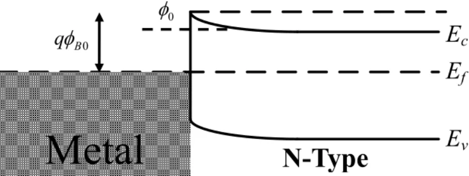
The metal-semiconductor junction was first reported by W. Schottky [13]. He reported that the metal-semiconductor junction can work as a rectifier by its statistic space charge induced potential barrier. The barrier is called Schottky Barrier. Fig. 2.1(a) is the band diagram of a Schottky junction in a non-equilibrium situation. Here, qmis metal work function, qsis semiconductor work function, qχ is electric affinity of semiconductor which is an intrinsic property of the crystal lattice, E0 is vacuum free-electron energy, Ef is the Fermi level which
depends on doping concentration, and Ec and Ev are conduction and valance band edge of
semiconductor. Besides, the most important parameter in metal-semiconductor junction is qBwhich indicates the difference between metal and semiconductor work function.
When the two materials are in touch with each other, a net flow of electrons or holes is induced through the junction in order to equalize the Fermi level. In non-equilibrium condition, elections in semiconductor have higher energy and attract by the metal, creating a depletion regime in the semiconductor, see Fig. 2.1(b). Under equilibrium condition, the magnitude of the energy step for N-type semiconductor which is called Schottky-barrier height is given by eq. (2.1), and for P-type is given by eq. (2.2).
, B n m q q (2.1)
, B p g m q E q (2.2) Here, Eg is the energy gap of the semiconductor. The sum of the two barrier-heights is shownin eq. (2.3), which equals to energy gap, i.e.,
B p, B n,
gq E . (2.3) When the electrons are going from semiconductor to metal, they will see a barrier which is called build-in potential Vbi. Here Vn is the energy difference between conduction band edge
and Fermi level.
,bi m s B n n
V q V . (2.4)
2.1.2 Effective of the Fermi Level Pinning
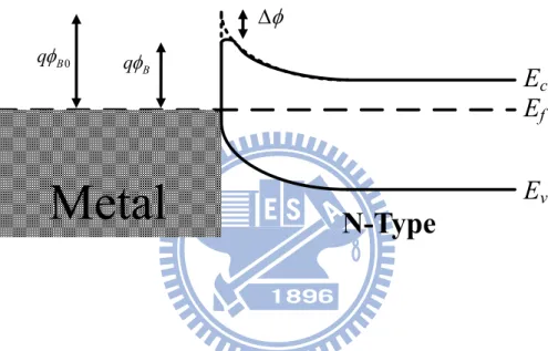
Because the lattice constant of the metal and semiconductor are different, at their junction surface, there are several surface states in the forbidden energy gap due to the presence of dangling bonds. The unpaired atom can be acceptor or donor type, which is determined by the charge neutrality condition. The neutral level 0is usually defined as the position of the Fermi level corresponding to electrical neutrality at the surface, see Fig. 2.2. Bardeen claimed that the surface state at the metal-semiconductor junction reduce the dependency of the Schottky-barrier height and the metal work function [14]. In Fig. 2.2(a), assuming no surface state existed; the Fermi level is located below the neutral level of the surface. A positive charge is stored in the surface state and the charge in the depletion region will be reduced accordingly to the neutrality condition. The reduction of the charge in the depletion region pushes the Fermi level toward 0and the barrier is lowered, see Fig. 2.2(b). Similarly, if the Fermi level is located above the neutral level, a negative charge is stored and increase of the positive charge in the depletion region pushes the Fermi level to 0. These phenomena are call Fermi level pinning and the Schottky barrier height is pinned in Eg-0.
0
B Eg
(2.5) In recent years, the Fermi level pining is also found in the high-κ metal-gate structure. The
new observations of Fermi level pining are explained by dipole effect. The details of dipole effect are complex that we do not emphasize it in this thesis.
2.1.3 Image-Force Lowering
Another phenomenon induces the Schottky-barrier lowering, which is the nature magnetic phenomenon, is the image-force lowering. This effect is the interaction between the electron and the positive image charge located in the metal. It modifies the band diagram and is according to Fig. 2.3. The magnitude of the barrier lowering is as follows:
1 3 4 2 3 8 s s q N (2.6) where ψs is the surface potential, N is doping concentration, εs is the dielectric constant of
semiconductor [15].
2.2 Current Transport Mechanism in Metal-Semiconductor Diode
There are several transport mechanisms in metal-semiconductor junction [16]: 1. The thermionic emission over the barrier.
2. The field emission (tunneling) through the barier. 3. Recombination in the depletion region.
4. Recombination in the neutral region (hole injection).
The first two mechanisms are the mainly mechanisms. When the metal-semiconductor junction under forward bias, as see in Fig. 2.4(a), the carriers are tunneling through the Schottky barrier or thermally emitting above the barrier. And the mechanisms are similar when in reverse bias is; see Fig. 2.4(b). Actually, most of the transport carriers have thermionic and field emission in the same time. Hence, the transport carriers have higher average energy in metal-semiconductor junction than in p-n junction.
2.2.1 Thermionic Emission Current
The thermionic emission model is first proposed by Bethe in 1942 [17]. He reported that the rate of emitted electrons from the semiconductor to the metal and from the metal to the semiconductor is proportional to the density of the state at the interface between the two materials. When the forward bias is applied, the thermionic emission current is present as:
** 2 B exp 1 thermionic q qV I AA T kT nkT (2.7) where A is the cross section of the junction, A** is the Richardson constant (for Si,
** 120
A for electrons and 30 for holes), n is ideality factor (about 1~1.2), k is the Boltzmann’s constant, T is the temperature by Kelvin coordinate, q is the basic charge of the electron, and Bis the effective Schottky-barrier height (contained the effect of image-force lowering).
2.2.2 Field Emission Current.
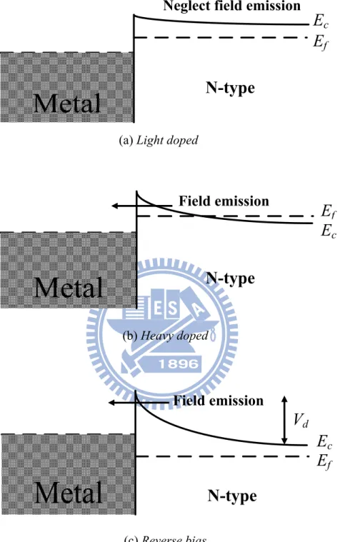
In Schottky contacts, the energy of carrier is lower than the Schottky barrier. If the carrier tunnel through the barrier from metal to semiconductor or the other, we called it field emission current. It may be possible under some circumstances, degenerate semiconductor under forward bias or for relative low doped substrate under negative bias [6]. The band bending next to the interface plays a crucial role since it determines the tunneling distance that is the region where the carrier is located within the energy gap with its wave function exponential decaying, see Fig. 2.5. The WKB approximation is following. Assuming a triangular barrier shape is used. The tunneling probability for an electron at energy ΔE from the barrier top is
1.5 0.5 00 2 exp 3 D E P E V (2.8a)where VD is the energy drop across the space charge region and E00 is N
We may know that the higher is E00; the large is ΔE which has a non negligible tunneling
probability. In lightly doped semiconductors, the depletion region width is large and the band bending is not strong enough to enable field emission, see Fig. 2.5(a). E00 is small and close to
the conduction band edge can tunnel through the barrier. And in heavy doped semiconductor, see Fig. 2.5(b), the narrow depletion region leads to large tunneling probability, which is consistent with large E00. When under reverse bias, the depletion region is narrower. It is
known that tunneling probability is larger, see Fig. 2.5(c). The tunneling current through the Schottky-barrier is give by eq. (2.9) [18].
2 2 3 * 8 exp 2 8 3 tunneling B B e I A m e h he (2.9) where h is Plank’s constant, A is the junction area, m* is the effective mass, and ξ is the electric field of the Schottky barrier. In real Schottky diode, most carriers transport through the junction by thermionic and field emission in the same time. This means that the carrier is on the higher position of the energy band diagram in transporting than in thermal equivalent condition. Based this phenomenon, carriers tunnel through the barrier which is called non-local tunneling.2.2.3 Measurement of The Schottky-Barrier Height
The simple and accurate Schottky-barrier height extraction method has been reported for a long time [15]. They are summarized as the following:
1. Current-Voltage (I-V) method
2. Current-Temperature (Activation-Energy) method 3. Capacitance-Voltage (C-V) method
4. Photoelectric measurement
The most appropriate method for our experiment is the activation-energy method due to the uncertain junction area of Schottky-barrier MOSFET. The method is derived from the
applied the nature logarithm on it. Assuming the device is N-type and the ideality factor is one, then we have
**
2 ln IF ln AA q B VF T kT (2.10) where the IF is the forward bias Schottky diode current, VF is the forward bias voltage. Andq(B-VF) is considered the activation energy. Then, we draw the ln(IF/T2) versus 1/T plot, see
Fig. 2.6. The Bis calculated by eq. (2.11), and m is the slope of curve. F B V k m n q . (2.11)
2.3 Introduction of the Schottky-Barrier MOSFET
In 1966, Nishi, first proposed a Japanese patent of Schottky-barrier MOSFET (SBMOS). But the first paper for SBMOS is published by Lepselter and Sze [19], who are the most important scholar in semiconductor technology. This is the first record for PtSi silicide PMOSFET. At that time, SBMOS performed poor performance so that it is concerned by nobody. Later in 1984, T. Mochizuki and K. Wise reported a n-channel MOSFET with Schottky source and drain [20]. After that the SB-CMOS have raised up their significance in the semiconductor devices., several advantages of the SBMOS had been reported gradually in the later years such as:
1. Better for devices scaling down. 2. Low parasitic source/drain resistance.
3. Low temperature processing for S/D formation. 4. Better control of short channel effect.
5. Reduced the floating body effect on SOI devices. 6. Reduced the latch-up susceptibility.
As shown in Fig. 2.7, when the conventional MOSFET is scaling down to a few nanometers, the doped S/D junctions are not abruptness so that the channel is easy to punch through. The
MOS capacitance. Hence, Schottky-barrier MOSFET is easier to scale down than conventional MOSFET. Besides, the series resistance is becoming as large as possible due to the scaling down of the junction area. When S/D changes from silicon to metal silicide, the series resistance becomes small. For example, a 60 nm thick PtSi sheet resistance is about 6 / .
2.4 The Operational Principle
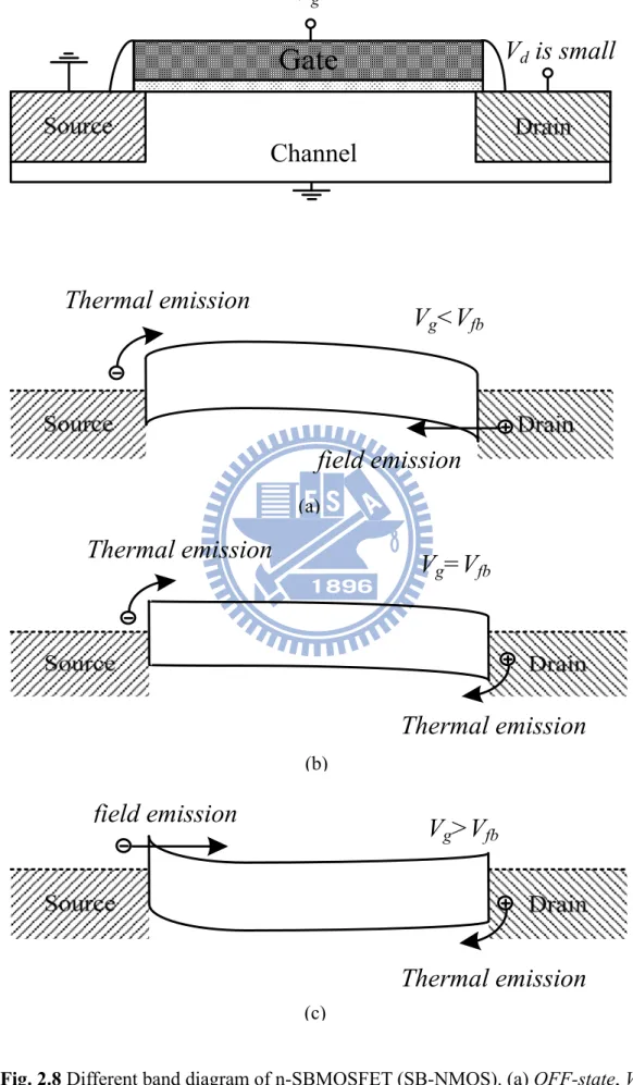
The typical SBMOS band diagram is shown in Fig. 2.8. In general, the carrier transport in SBMOS is so called “ambipolar”. When n-SBMOS or SB-NMOS is at OFF-state, the electrons in the source side see a thick and high barrier so that they can only thermionic emit over the barrier instead of tunneling. Under this situation, the thermionic current by electrons is quite small that reduced the OFF-state drain current. But actually, the OFF-state drain current is quite large due to holes injection in the drain end. In the drain side, holes see a thin Schottky barrier and are easy to tunnel through the barrier. That produced a large drain leakage current, see Fig. 2.8(a). While in the ON-state, the electrons see a thin Schottky barrier that contributed ON-state drain current, see Fig. 2.8(c). Because of the two carriers transport characteristic just like bipolar junction transistor, we call it “ambipolar transport”. Besides, in Fig. 2.8, the flatband voltage (Vfb) presents the gate voltage which makes the
lateral potential from channel to source become flat. We combined the band diagram with the gate voltage and divided the operational condition in three parts. When Vg<Vfb, SB-NMOS is
at OFF-state, as Fig. 2.8(a). Electrons see a thick barrier in the source side and holes see a thin barrier in the drain side that produced a large off leakage. When Vg=Vfb, both in source and
drain barrier are thick, carriers can only thermionic emit over the barrier. In this state, the drain current is very small, see Fig. 2.8(b). When Vg>Vfb, SB-NMOS is at ON-state, as Fig.
2.8 (c). Most of electrons in the source side are easy to tunnel through the thin barrier, which produced a large on current. These transport mechanism is different from the conventional MOSFET. We note that the on current is determined by the source side barrier height. If the
barrier is short or thin, the electrons are easy to thermionic emit above the barrier or tunnel through the barrier that produces large drive current. Besides, the off current is dominated by the drain side barrier height. It is important to increase the drain side barrier height so that the OFF-state leakage current will be decreased.
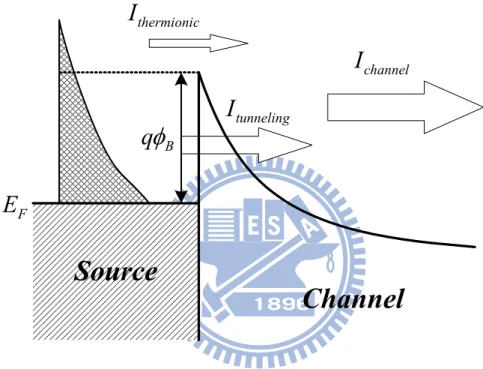
In real Schottky-barrier MOSFETs, the ON-state current is contributed by both thermionic emission and field emission components. We describe the total current as eq (2.12). Some of the carriers get enough energy so that they can thermal emit over the Schottky barrier.
channel thermionic tnnneling
I I I . (2.12) The carrier transmission model is illustrated in Fig. 2.9. Most of carriers tunneled through the barrier. Thus, the tunneling current is larger than thermionic current, which is the major carrier transport mechanism in the Schottky-barrier MOSFET.
2.5 The Challenges and New Technologies of SBMOS
2.5.1 Reduction of Schottky-Barrier Height
In section 2.1.2, we have reported the Fermi level pining effect. This effect induces the Schottky-barrier height pinned in the same value. No mater how we change the metal, the Schottky-barrier height is unchanged. In order to reduce the barrier height, some methods have been reported [21], see Fig. 2.10. For examples, W. Saitoh reported the results of barrier height reduction. When the channel length is short and the Schottky-barrier height is as low as
0.1eV for N-type and 0.2eV for P-type, the performance of SBMOS is better than conventional
MOSFET [18], see Fig. 2.11. Because of the Fermi level pinning, if we would to achieve an absolutely low Schottky-barrier height, we need a perfect junction interface and small work function difference between metal and semiconductor. This is nearly impossible. However, some researchers brought up some methods that we can get a low Schottky-barrier height equally. One of the methods is depositing an insulator layer between the silicon and the metal
junction, see Fig. 2.10 (a). The dangling bond on the silicon substrate will skip by this layer and the original Schottky barrier is lowering.
The other method is dopant segregation implantation method; see Fig. 2.10 (b) [23]. Before silicidation, a high dose of low energy dopant is implanted in the S/D region to the silicon interface. This high dose layer induces a high electric field so that the barrier will become thinner. This layer is a thin tunneling barrier which works like an insulator layer. Thus, the carriers are easy to tunnel through the barrier toward the channel. The As or S implantation has been reported to reach a very low effective barrier of 0.1eV [24]. Nowadays, the dopant segregation implantation technology is used widely in novel semiconductor industry.
2.5.2 Modern Technologies for SB-CMOS
In recent year, some different materials and architectures have been used for improving the performance of the integrated circuit, such as rare element silicide in S/D region, silicon on insulator and high-κ dielectric in gate stack. A lot of new materials have been published for the S/D silicide. For SB-NMOS, nickel (Ni) and platinum (Pt) is used. For SB-PMOS, erbium (Er) and ytterbium (Yb) is used. The Schottky-barrier height for SB-NMOS is about
0.15~0.3eV, and 0.27~0.4eV for SB-PMOS. Because of the spike barrier blocks most of the
carriers, the drain current of SBMOS is smaller than conventional MOSFET. Besides barrier reduction, someone applied the process strained silicon (PSS) technology on SBMOS. In typically, contact etch stop layers (CESL) technology is adopt by some companies [25-26].
In order to conflict the short channel effect, some structures are brought up for SBMOS, just like dual-gate structure, FinFET [27] and Vertical MOSFET. Besides, someone has reported the hot-electron generation rate in SBMOS [28]. It was concluded that the generation rate in SBMOS is better than conventional MOSFET. For this reason, we can apply metal S/D in the flash memory which will cause large hot electron injection rate.
Fig. 2.1 Energy band diagram of a Schottky contact (a) under non-equilibrium condition (b) equilibrium condition.
(a) B q
Metal
i q
, B n q
, B p q
Ef
(b)Ec
Ef
Ev
Metal
Semiconductor
E0
E
fEc
Ev
s q
Ef
m q
m qDepletion region
Fig. 2.2 Energy band diagram of a Schottky contact (a) without and (b) with the effect of surface states. The Fermi level is pushed to0.
Without effect of surface states
(a)
Ec
Ef
Ev
0 Bq
0
N-Type
With effect of surface states
Ec
Ef
Ev
Pinning the Fermi levelB q Barrier lowering
N-Type
0 0 B q (b)Fig. 2.3 Image force induced Schottky-barrier lowering.
N-Type
Ec
Ef
Ev
0 B q B q
Fig. 2.4 Carrier transport mechanism of the Schottky contact in N-type semiconductor. (a) under forward bias (b) under reverse bias.
E
cEf
Tunneling Thermal emission DiffusionVa
B qV
aForward Bias
Reverse Bias
Thermal emission TunnelingEc
Ef
Va
Drift (b) (a)Fig. 2.5 Band diagram to deduce the probability of field emission (a) light doped condition (b) heavy doped (degenerate) condition (c) under reverse bias condition of a junction between n-type semiconductor and metal.
(a) Light doped
Ec
E
fNeglect field emission
N-type
(b) Heavy dopedN-type
Field emission
E
fEc
Field emission
E
fE
cVd
N-type
(c) Reverse biasFig. 2.6 Extracting the Schottky-barrier height by Activation-Energy method.
2.50
2.75
3.00
3.25
3.50
-33.2
-32.8
-32.4
-32.0
-31.6
In(I
D/T
2) (AK
-2)
Measurement Temperature 1000/T (K
-1)
VF= 0.1V n= 1.1 Slope= -1.2836 BN= 0.202 eVSlope=1.2836
0.202 Bn eV , 1000/T (K
-1)
Fig. 2.7 The device structures (a) conventional MOSFET (b) Schottky-barrier MOSFET.
Oxide
Contact
Side Wall Spacer
(a)
(b)
Fig. 2.8 Different band diagram of n-SBMOSFET (SB-NMOS). (a) OFF-state, V <V
V
dis small
Channel
(a)Thermal emission
Vg<Vfb
field emission
(b)Vg=Vfb
Thermal emission
Thermal emission
(c)Vg>Vfb
Thermal emission
field emission
Vg
Source
Bq
thermionicI
tunnelingI
FE
Channel
channelI
Fig. 2.9 Current components in the source to channel interface of Schottky-barrier nMOSFETs.
Fig. 2.10 Schottky barrier height reduction technology (a) with insulator layer (b) with dopant segregation implantation.
Ec
E
fE
v (a)Vg low
Vg high
(b)(a)
(b)
Fig. 2.11 Drivability of Schottky barrier MOSFET as a function of Schottky-barrier height for (a) N-type and (b) P-type devices [18].
Chapter 3
Device Preparation and Basic Characteristics
In advanced VLSI technology, the high-κ dielectric with metal gate, metal S/D SBMOS, process strained silicon and silicon-on-insulator technology are the most popular nowadays. Some of them are good for devices scaled down and conflicting short channel effect as we mentioned in the above chapter. In section 2.5.1, we demonstrated that the novel technologies for SBMOS to overcome poor performance due to high Schottky barrier height and small driving current. The most simple and popular method is dopant-segregation-implantation (DSI) technique which is developed by B.Y. Tusi [12]. On the other hand, the optimized method is first reported by A. Kinoshita [23]. In this chapter, first, we focus on how to optimize the Schottky barrier MOSFET with DSI technology and its manufacturing process. Then, we introduced our experimental setup. Finally, we demonstrate the basic characteristics of the sample devices.
3.1 Devices Preparation
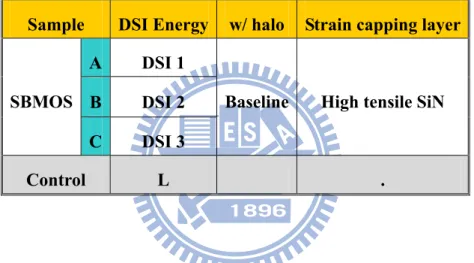
In order to simplify the experiments, we controlled that the gate channel of the devices are in the same orientation of <110>/(100) which their gate oxide thickness are 1.4nm. The channel lengths are from 10μm to 0.06μm. The SBMOS with DSI fabrication process flow bases on the United Microelectronics Corporation (UMC) 65-nm technology node and is illustrated in Fig. 3.1. Following the gate stack formation, optimized offset spacer, halo and DSI implants were introduced. Then disposable spacer and deep S/D implant were performed in order to suppress the junction leakage. After disposable spacer removal, NiPt silicidation process was applied on either N or PMOSFET with DSI for its better immunity against line width effect and less silicon consumption. On the other hand, strain capping layer as high tensile SiN was performed to optimize the driving current. The split of the devices for both N and PMOS are figured in Fig. 3.2(a) and the cross-section TEM picture is shown in Fig. 3.2(b).
Besides, the conventional MOSFET were also prepared as control sample, see Fig. 3.2(a). The arsenic was implanted as a high doped layer between the S/D to substrate region and the doping concentration reached 2.5×1020cm-3. The depth of the interface between NiPt silicide and silicon is about 18nm. The halo is implanted for suppressing the severe short channel effect and high leakage current [25]. In order to optimize the DSI energy, different implant energies are performed, see Table 1. Sample C was implanted with the highest DSI energy, and sample A was with the lowest energy. The order is
1 2 3,
DSI DSI DSI or A B C (3.1)
The Ion-Ioff characteristic and source/drain sheet resistance are shown in Fig. 3.3 [25]. Sample
B has the optimized Ion-Ioff characteristic. Besides, they all have the advantage of SBMOS,
which is the lower source and drain sheet resistance than conventional MOSFET, is shown in Fig. 3.3(b). The sheet resistance is about 19% lower.
3.2 Experimental Setup
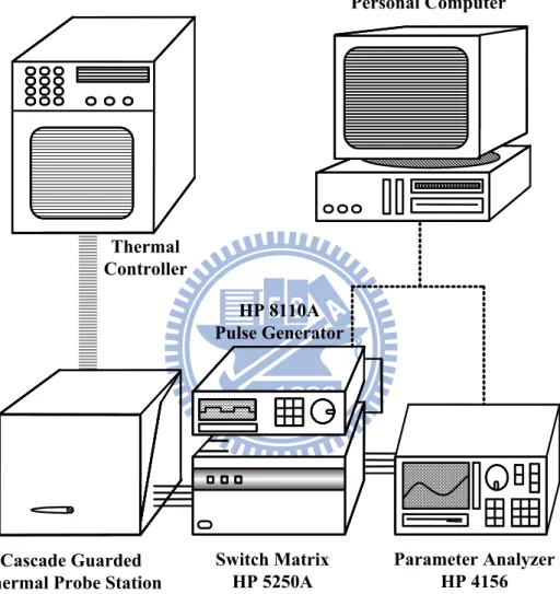
The experimental setup for the current-voltage measurement of devices is illustrated in Fig. 3.4. Both of the intrinsic and degradation behaviors of the devices can be achieve by this system. Each of the analyzers are connected by the co-axial or tri-axial cable, included the semiconductor parameter analyzer (HP 4156C), the low leakage switch mainframe (HP E5250A), the Cascade guarded thermal probe station, and a thermal controller. This facility provides an adequate capability for measuring the low leakage devices I-V characteristic. On the other hand, for precisely measuring of capacitance-voltage characteristic of the devices, LCR Meter (Agilent-HP 4284A) has been added. It provides the testing frequency from 20Hz to 1MHz for AC voltage. These analyzers are controlled by the corresponding software in the PC. Our group developed a control system in HT-Basic language. Through IEEE-488 (GPIB) cable, we can directly give the order to each analyzer. By the above system, the I-V and C-V characteristics of the MOSFET devices can be precisely performed.
3.3 Basic Characteristics of the Schottky-Barrier MOSFETs
In this section, we present the basic characteristics of the SBMOS, such as band diagram, short channel effect, current-voltage characteristics, and effective Schottky- barrier height. Then, we make a conjecture to the main factor of the SB-MOSFET characteristics.
3.3.1 Band Diagram of DSI-SBMOS
The band diagram of conventional Schottky barrier MOSFET is shown in the above chapter, see Fig. 2.8. However, the Schottky barrier MOSFET with dopant segregation implantation (DSI-SBMOS) is modified by the conventional SBMOS with the arsenic doped between S/D and substrate interface, see Fig. 2.10(b), and our sample devices split is shown in Fig. 3.2(a).
In order to understand the carrier transport mechanism, the band diagram of the DSI-SBMOS in the lateral direction is important. We compared the conventional SBMOS with the DSI-SBMOS as shown in Fig. 3.5 at small drain bias. The arsenic with high doping concentration induced a high electric field near the S/D to channel interface by the barrier adjustment method in [15]. Thus, the band diagram is pulled down by this high dose layer, which leads to thin down the Schottky barrier. It is called dopant segregation implantation (DSI) technique. In this optimized process, the barrier becomes the shape of the spike and leads to high tunneling current. We define that the barrier between source to channel interface and the lowest conduction band edge near the source side as Schottky barrier or tunneling barrier, and the barrier between the two lowest conduction band edges near S/D side in the channel as channel barrier, we marked them in Fig. 3.5(b). On the other hand, the holes in the valance band see a higher barrier that they are not easy to emit through it. This suppressed the OFF-state current and improved the current-voltage (I-V) characteristic.
3.3.2 Basic Characteristics of DSI-SBMOS
Figure 3.6 shows the short channel effect of our devices, and sample B is the optimized sample. In short channel region, we can see that the lager the DSI energy is, the smaller the VTH is. Fig. 3.7(a) is the drain current versus gate voltage plot (ID-VG). The drain current
versus drain voltage curve (ID-VD) is shown in Fig. 3.7(b). Fig. 3.8 shows the ID-VG plot at
|VD|= 0.1V with different DSI energy, both N and PMOS, the larger the DSI energy is, the
larger the OFF-state current (Ioff) is.
3.3.3 Current Flow Mechanism
The carrier transport mechanism is an important issue for Schottky barrier MOSFETs. Some paper explained the current transport mechanism in the ON-state by operational temperature variation [29], but the analyzed process is ambiguous. In order to understand the refined current transport mechanism, we investigated the effective Schottky-barrier height profiles.
The most important parameter for Schottky barrier MOSFET is the Schottky barrier height which blocks most of the injection carriers from source to channel as we have mentioned in the above chapter. In order to measure the Schottky barrier height, we applied the “Activation-Energy Measurement” which is reported by SZE [15] and we have reported in section 2.2.3. In comparison with the Schottky diode, SBMOS is a four-end device. So, we define the measured barrier height as effective Schottky-barrier height, B eff, , and is measured from source to channel junction as the following:
, , ( , ).
B eff B eff V VG D
(3.2) The parameter is a function of the gate and drain voltage due to the two voltages will influence the barrier height and thickness [30]. Fig. 3.9 shows the calculated effective Schottky barrier height of SB-PMOS with sample A and B. When the SB-PMOS operates in
very positive bias, by ambipolar characteristic, the transport carriers, which are electrons from drain end, transport by field emission (tunneling) mechanism and see a very thick barrier blocked some of carriers in the conduction band. That contributes to a very high effective Schottky-barrier height form difficult tunneling. If the gate bias is increasing positively for PMOS, the tunneling barrier is thinner that are easy to tunneling. Thus, the top of the effective Schottky-barrier height is decreasing as gate bias is increasing positively. As the gate voltage is increasing negatively, the SB-PMOS entered subthreshold region. In this region, the SB-PMOS with dopant segregation implantation produces a thin tunneling barrier which is easy for holes to tunnel through in the valance band. However, the carriers tunneled through the tunneling barrier, and then they see a lower channel barrier. When the gate bias increases, the channel barrier decreases. This makes the effective Schottky-barrier decrease. As in Fig. 3.9, the effective Schottky-barrier height is linear to gate voltage, which means the current is contributed by thermionic emit through the channel barrier. Hence, the subthreshold current is quite small that produces a small subthreshold swing, which is called DIBL-like effect. When the gate bias is larger than threshold voltage (in Fig. 3.9, VG -VTH=0), a negative effective
Schottky-barrier height formed. The band diagram is illustrated in Fig. 3.10. The dashed line is the OFF-state conduction band edge and the solid line is ON-state for NMOS [30]. In this region, the channel barrier is lower than flat band (Vfb). Most of the transport carriers tunneled
through the tunneling barrier and see a negative channel barrier. Hence, the negative Schottky-barrier height is formed. Therefore, the tunneling current is the main transport method in the ON-state. It is worthy to be mentioned that the carriers are non-local tunneling here.
Based on the above, the external bias (VD ,VG) can only vary the channel barrier but
Schottky barrier. This implies that the barrier pinning position is change to the interface between DSI layer and bulk effectively. Thus, the effective Schottky-barrier height presents the channel barrier variation. On the other hand, by Fig. 3.9, we concluded that the larger the DSI energy is, the lower effective Schottky barrier height is.
Another important issue for current transport mechanism is body effect. Fig 3.11 is the effective Schottky barrier height of SB-PMOS (B eff, )with different substrate bias (VB). When
VB is decreasing toward minus region for PMOS, the threshold voltage is decreasing positively.
And the channel barrier will be raised up, see Fig. 3.12. As in the above words, the top of the effective Schottky-barrier height is from the minority carrier tunneled through the barrier. For PMOS, electrons see a raised conduction band edge that makes the effective Schottky-barrier height increase. In addition, the effective Schottky barrier height is independent on channel length, see Fig. 3.13. The two devices (0.36 and 0.5μm) have the same threshold voltage. The comparison of conduction band diagram is shown in Fig. 3.14, including conventional MOSFET, conventional SBMOS and DSI-SBMOS. By the effective channel barrier pinning, the tunneling barrier is independent to length.
3.3.4 Conductivity on DSI-SBMOS
We have explained the process of dopant segregation implantation on Schottky-barrier MOSFET. Also, the operational carrier transport mechanism is performed by effective Schottky-barrier height. The DSI-layer will pull down the Schottky barrier that enhances the carrier tunneling probability in the source side. Some researcher had verified this phenomenon by conductivity theory [31]. By a modified one-dimensional Poisson equation:
2 2 2 0 seg f f g bi si e x N d dx (3.3)where f is the surface potential, g is the gate potential and bi is the build-in potential. And, λ is the relevant length scale on which potential variations are being screened, as eq. (3.4). si ox si ox d d . (3.4)
channel interfaces. The charge ρ(x) in and current through the channel is calculated employing the non-equilibrium Green’s function formalism, where the equation for the charge is solved self-consistently with eq. (3.3). After self-consistency is reached, the current is computed according to eq. (3.11).
2 d s d e I W dE T E f f h
(3.5) where fs,d are the Fermi distributions of source/drain and T(E) is given by the Fisher-Leerelation which is the transmission function for carriers moving from source to drain [32]. The conductivity ( ) is contributed by eq. (3.6).
2 2 2 | | 2 | | e t r . (3.6) Here, t is the transmission and r is the reflection coefficient. It is assuming that the first subband contributes most to the current. So, the expressions for charge and current are averaged over the direction of W only. Besides, higher subbands are accounted for by a numerical factor that leads to higher tunneling energy [33]. Hence, ballistic transport coefficient is assumed to give an upper estimate of the possible device performance. This is the first theory on ballistic transport [32] and leads to Natori’s backscattering theory that we will introduce in the next chapter.
3.5 Summary
We make a summary of the relations between DSI energy and basic characteristics which we have mentioned in the last section. When the DSI energy is increasing, the VTH is
decreasing, Ioff is increasing and B eff, becomes lower. This is due to the increasing of the DSI
energy, the lowest of the conduction band edge of the channel will be far from the S/D to channel interface, see Fig. 3.15 (a), and channel barrier will be lower when drain voltage is applied. Similarly, the B eff, is the channel barrier which influences the carrier transport in the devices. In other words, the VTH and B eff, are determined by the channel barrier. Further, the
holes see a lower barrier that they are easy to emit above it. As shown in Fig. 3.15 (b), the barrier is lower when DSI energy is larger. By these inferences, the channel barrier is more significant than Schottky barrier in DSI-SBMOS. Finally, it is important for us to understand the carrier injection phonemes and the backscattering probability in front of the channel barrier.
STI Formation
Poly Gate Stack Formation Offset Spacer Formation Halo I/I
Dopant Segregation Implantation (DSI) Disposable Spacer Formation
Deep S/D Implantation RTP Annealing
Disposable Spacer Removal NiPt Silicidation
(b)
Fig. 3.2 (a) Device split of Schottky-barrier MOSFETs with DSI NiPt silicide and conventional MSOFET and (b) its crocess-section TEM picture with the shortest length 35nm [25].
(a)
SiN
DSI
Spacer
Sample DSI Energy w/ halo Strain capping layer
A DSI 1
B DSI 2
SBMOS
C DSI 3
Baseline High tensile SiN
Control L .
Table 3.1 Splits of SBMOS with different DSI energies. The DSI energy relation is DSI1
(a)
(b)
Fig. 3.3 (a) The Ion-Ioff characteristics of Sample A, B and C. Sample B has the
optimized characteristic. (b) All of them show the reduced S/D sheet resistance [25].
Cascade Guarded Thermal Probe Station
Personal Computer Thermal Controller HP 8110A Pulse Generator Switch Matrix HP 5250A Parameter Analyzer HP 4156
Fig. 3.5 Conduction band diagram of the (a) conventional SBMOS (b) SBMOS with dopant segregation implantation (DSI-SBMOS) when VD is small bias.
(a) (b)
Source
Source
Drain
Drain
Channel
Channel
V
Dsmall
V
Dsmall
Schottky barrierChannel barrier
-1.0
-0.5
0.0
0.5
1.0
10
-1210
-1110
10
-10 -910
-810
-710
-610
-510
-410
-310
-210
-1 Length=60nm S.S. = 138mV/V DIBL= 84mV/VGate Voltage, V
G(
V
)
I
D(
A/
m
)
Solid : |VD|=1V Hollow: |VD|=20mV Length=60nm S.S. =105mV/V DIBL=152mV/V 10-12 10-11 10-10 10-9 10-8 10-7 10-6 10-5 10-4 10-3 Sample B SB-NMOSI
D(
A/
m
)
Sample B SB-PMOS (a) -1.0 -0.5 0.0 0.5 1.0 0 200 400 600 800 1000 0 200 400 600 800 1000Drain current,
I
D(
A/
m
)
NMOSDrain current,
I
D(
A/
m
)
Gate Voltage, V
G(
V
)
Sample B Lgate= 60nm |VD|= 0.25~1.5V |Step Vlotage|= 0.25V PMOS (b)-1.0 -0.8 -0.6 -0.4 -0.2 0.0 0.2 0.4 10-13 10-12 10-11 1010-10 -9 10-8 10-7 10-6 10-5 10-4 Sample A Sample B
Drain curent,
I
D(
A/
m
)
Gate Voltage, V
G(
V
)
SB-PM OS Length = 60nm |VD|=0.1VCircle : Larger DSI energy
(a) -0.4 -0.2 0.0 0.2 0.4 0.6 0.8 10-11 1010-10 -9 10-8 10-7 10-6 10-5 10-4 10-3 S am ple B S am ple C
Drain current,
I
D(
A/
m
)
G ate V oltage, V
G(
V
)
S B -N M O S L en g th = 6 0 n m |VD|= 0 .1 V C ircle : L a rg er D S I en erg y (b)Fig. 3.8 Drain current versus gate voltage curve (ID-VG) with different DSI energy when
-0.6 -0.4 -0.2 0.0 0.2 0.4 0.6 0.8 -0.1 0.0 0.1 0.2 0.3 0.4 0.5 Sample A, |VD|=0.1V Sample A, |VD|= 1V Sample B, |VD|=0.1V Sample B, |VD|= 1V Effecti ve S ch ottky-Barrier Height, B,e ff
(
eV)
Gate Voltage Shift, V
G-V
TH(
V
)
SB-PMOS W/L=1/0.06
DSI energy : B >A
Fig. 3.10 The conduction band edge of SBMOS with different bias condition. The dash line is OFF-state and solid line is ON-state.
DSI layer
OFF-State
-1.0 -0.8 -0.6 -0.4 -0.2 0.0 0.2 0.4 -0.1 0.0 0.1 0.2 0.3 0.4 0.5 W/L=10/0.06 |VD|=0.1V Sample B SB-PMOS VB= -0.3 VB= 0.0 VB=+0.3 VB=+0.5 E ff ect ive Schot tky-b arri er H ei ght B,ef f
(
eV)
Gate Voltage, V
G(
V
)
Fig. 3.11 The effective Schottky-barrier height of SB-PMOS with different bulk bias (VB).
Source
Drain
(a)
Source
Drain
(b)
Fig. 3.12 The band diagram for different substrate bias of (a) VB=0 (b) VB<0 for
Schottky-barrier pMOSFETs.
V
B=0
|V
D|>0
|V
D|>0
-0.4 -0.2 0.0 0.2 0.4 0.6 0.8 1.0 -0.1 0.0 0.1 0.2 0.3 0.4 B,peak=0.32eV SB-PMOS Sample B Width=2m |VD|=0.1V
Gate Voltage, V
G(
V
)
L= 0.5m L=0.36mEffective Schottky-Barrier Height
B,ef f (eV
) SB-NMOS Sample B Width=2m |VD|=0.1V B,peak=0.32eV -1.0 -0.8 -0.6 -0.4 -0.2 0.0 0.2 0.4 -0.1 0.0 0.1 0.2 0.3 0.4 L= 0.5m L=0.36mFig. 3.13 The effective Schottky-barrier height of both N and PMOS with different channel length.
Fig. 3.14 The conduction band edge with different devices (a) Conventional SBMOS (b) DSI-SBMOS (c) Conventio-nal MOSFET. The solid line is short channel and dash line is long channel devices.
Source
Drain
(a) (b) (c)V
G>0
V
D>0
Fig. 3.15 The band diagram of the DSI-SBMOS with different DSI energy in (a) ON-state (b) OFF-state. The DSI energy of the blue line is lower than red line. The dash line is the conventional SBMOS band diagram.
(a) (b)
![Fig. 2.11 Drivability of Schottky barrier MOSFET as a function of Schottky-barrier height for (a) N-type and (b) P-type devices [18]](https://thumb-ap.123doks.com/thumbv2/9libinfo/8410757.179834/37.892.206.674.235.968/drivability-schottky-barrier-mosfet-function-schottky-barrier-devices.webp)