國
立
交
通
大
學
光電工程研究所
碩
士
論
文
氧化銦錫奈米結構兆赫頻段光學特性與電性之研究
Terahertz spectroscopic studies of ITO nanostructures
研 究 生:曾冠儒
指導教授:潘犀靈 教授
氧化銦錫奈米結構兆赫頻段光學特性與電性之研究
Terahertz spectroscopic studies of ITO nanostructures
研 究 生:曾冠儒 Student:Kuan-Ju Tseng 指導教授:潘犀靈 Advisor:Ci-Ling Pan 國 立 交 通 大 學 光電工程研究所 碩 士 論 文 A Thesis
Submitted to Department of Computer and Information Science College of Electrical Engineering and Computer Science
National Chiao Tung University in partial Fulfillment of the Requirements
for the Degree of Master
in
Computer and Information Science June 2010
Hsinchu, Taiwan, Republic of China
氧化銦錫奈米結構兆赫頻段光學特性與電性之
研究
學生:曾冠儒 指導教授:潘犀靈教授 國立交通大學光電工程研究所 摘要 我們使用兆赫波時域光譜的光學量測方法去探討氧化銦錫奈米 柱的光學特性和電性。首先,我們分別量測了樣品以及基版的兆赫波 時域訊號,藉由傅立葉轉化成頻域訊號後分析可以得到不同厚度氧化 銦錫奈米柱 0.2~2(THz)複數的折射係數,而複數的折射係數可以轉 換成複數的導電率,以 Drude-Smith 模型來擬合實驗的導電率。我們 得到樣品的電漿頻率,其值為 74~396(radTHz),載子的散射時間為 34~68(fs/rad),另外,Drude-Smith 模型的電子碰撞參數 c 大於 -0.4。 這種光學量測方法可以得到各種奈米結構材料的電性,我得到對應的 載 子 漂 流 率 跟 載 子 濃 度 , 分 別 為 100~400 cm2 /Vs 和 0.05×10¹⁹ ~1.5×10¹⁹ 。和傳統的霍爾量測或四點探針比起來,兆赫波時 域光譜的光學量測方法是非接觸式且不會破壞樣品的表面,藉由 Drude-Smith 模型的輔助我們可以得到奈米結構材料的電性。Terahertz spectroscopic studies of ITO
nanostructures
Student: Kuan-Ju Tseng Advisor: Prof. Ci-Ling Pan
Department of Photonics and Institute of Electro-Optic Engineering, College of Electrical Engineering National Chiao Tung University
Abstract
We have investigated the optical and electrical properties of Indium Tin Oxide (ITO) nanocolumns by using terahertz time domain spectroscopy (THz-TDS). First, we measured the THz time domain waveform for both sample and reference. After transforming into frequency domain, we extracted the frequency dependence complex refractive index. Second, we can determine the experimental complex conductivity by complex refractive index. With fitting the real and image part of conductivity by Drude-Smith model, we finally extract the fitting parameters such as plasma frequency, scattering time and Drude-Smith constant c.
In this work, we obtained the plasma frequency of ITO nanocolumns is around 74~396 radTHz, and the scattering time is around 34~68 fs. Moreover, the electron original velocity fraction coefficient is larger than -0.4. The electrical properties of ITO nanocolumns derived from non-contact optical techniques have been determined. The mobility is 100~400 cm2/Vs and the carrier concentration is 0.05×10¹⁹~1.5×1019 cm-3. Comparing with conventional Hall or four probe measurement, THz-TDS is a non-contact method and the electrical properties of nanostructure material can be derived from the experimental conductivity by fitting
誌
謝
碩士班的日子已經進入尾聲,兩年的時間在酸甜苦辣中度過,首先要感謝潘 老師的指導,不僅僅是在研究方面,讓我瞭解做事情該有的方法和態度,雖然沒 有誇張到在血淚交織下完成學業,但是,這也算是個艱苦的過程吧!古人說:「不 經一番寒徹骨,焉得梅花撲鼻香。」現在我已經能隱隱約約聞到梅花的香味了。 還記得第一次在 meeting 中報告文獻,用糟糕兩個字還不足以形容我的表現, 這算是這兩年我印象最深刻的事情吧,從什麼地方跌倒就要從那裡站起來。現在 我的報告雖不能說有多完善,相信也算毫不馬虎了吧!沒有潘老師那時候嚴厲的 指導,我可能也不會這樣痛定思痛的反省自己。再來要感謝的是 Moya 學長,雖 然你在我升上碩二不久就離職了,但還是不時的關心我實驗的進展,你亦師亦友 的指導,讓我的研究生活輕鬆不少;也要感謝 Mika 學長,讓我體會到做研究需 要的紀律與法則;再來是阿達學長,沒有你我可能就不會自己動手寫程式;最後 一定要提到我的直屬 choppy 學長,碩一那一年我從來都沒辦法理解為什麼你要 用生命做實驗,隨著你畢業我升上碩二後,我發現我漸漸認同很多你的想法,原 來做研究是這麼回事阿!實驗室的成員睿茵、聖司、承山、楙翔、宏哲、韋翔、 志軒和承翰,謝謝你們讓我的研究生涯增色不少,讀萬卷書行萬里路,要感謝的 人太多,那就謝天吧! 家人的支持永遠是一個人最大的力量,父親、母親、弟弟和妹妹,最愛你們 了,現在我只有一句話要說:「我要回家了」。最後的最後,從大學就陪伴我的女 朋友麗恩,相信我們應該也像家人一樣,不需要道謝了吧,在這裡獻給所有我愛 的人最深的祝福。
Contents
Chapter 1 Introduction
1.1 THz radiation………...01
1.2 Nanostructured materials……….02
1.3 Transparent Conductive Oxides (TCOs)……….03
1.4 Motivation for THz measurement………...03
Chapter 2 Theoretical method
2.1 THz time-domain spectroscopy………..……….042.1.1 THz time-domain spectroscopy.……….04
2.1.2 Propagation of electromagnetic wave……….04
2.1.3 Refraction index extraction……….11
2.1.4 Optical conductivity………15
2.2 Fourier transform infrared spectroscopy………….………25
2.2.1 Fourier transform infrared spectroscopy………25
2.2.2 Complex dielectric function………...25
Chapter 3 Experimental setup
3.1 THz time-domain spectroscopy…..……….313.1.1 Ultrafast laser system……….………..31
3.1.2 THz time domain spectroscopy (transmittance)…….…….33
3.3 Sample preparation………..40
3.3.1 ITO nanorods………...40
3.3.2 SEM results………..44
Chapter 4 Results and discussion
4.1 Extraction of complex refraction index………...…………494.1.1 THz field in time-domain ………....………...49
4.1.2 THz spectrum in frequency domain ………..……….53
4.1.3 Optical constants of the substrate………..…..57
4.1.4 Complex refractive index of ITO nanorods…...61
4.2 Extraction of electrical properties………...66
4.2.1 Complex conductivity and fitting results…...………..66
4.2.2 Mobility and carrier concentration………..72
4.3 Extraction of electrical properties by FTIR……….74
4.3.1 Reflectivity spectrum in frequency domain……...………74
4.3.2 Fitting results and discussions…..………….………...….75
Chapter 5 Conclusions
5.1 Conclusions……….815.2 Continuous work……….81
List of Figures
1.1 The spectral range of electromagnetic waves……… 01
2.1 Figure of ray optics model for thick sample……….. 05
2.2 THz time-domain waveform transmitted the 525μm silicon substrate.. 06
2.3.1 The diagram of the reference………. 07
2.3.2 The diagram of the sample……… 07
2.4 THz time-domain waveform transmitted the 323nm ITO rod on 525μm silicon substrate………. 09
2.5 Three phase (air/sample/substrate) using multiple reflection to calculate the transmittance……… 10
2.5.1 (a) Original transmittance of air in time domain (b) In frequency domain……… 12
2.6 The contour plot of error function for n, k………. 13
2.6.1 Real part of refractive index (left) and image part (right) calculated in Wolfarm Mathematica for example………... 13
2.6.2 Extraction of complex refractive index step by step………. 14
2.7 Complex refractive index determined complex conductivity of 687nm ITO nanorod………... 17
2.8 The complex conductivity of 483nm ITO thin film………... 20
2.8.1 Mobility and concentration extraction step by step………... 21
2.8.2 Conductivity of the InN film. Solid and dashed lines correspond to the calculated results based on the simple-Drude model………... 24
2.8.3 Conductivity of the InN nanorods……….. 24
2.9 Reflective signal of silver and Silicon wafer from FTIR………... 26
2.10 Reflectance of Silicon wafer from FTIR……… 27
2.11 Electrical parameters extract by FTIR step by step………... 30
3.1 The setup of Kerr-lens mode-lock (KLM) titanium sapphire ultrafast laser……… 32
3.2.1 Transmittance THz time domain spectroscopic system………. 33
3.2.2 Structure of photoconductive antenna and silicon lens……….. 34
3.2.3 THz (a) time-domain waveform (b)corresponding power spectrum in the air……….. 36
3.3 The visible and UV spectra of liquid water………... 37
3.4 THz (a)time-domain waveform (b)corresponding power spectrum in the air with humidity under 5%………. 38
3.5 The setup of Fourier transform infrared spectrometer………... 39 3.6 (a) Epitaxial structure of a single-junction GaAs solar cell (b) 41
Schematic of a GaAs solar cell fabricated employing ITO
nanocolumns[2]……….
3.7.1 The picture of chamber……….. 42
3.7.2 View of the chamber……….. 42
3.8 ITO rod grown on Silicon wafer……… 43
3.9 THz experiment of sample and reference……….. 44
3.10 687nm ITO nanocolumns with cross-sectional view of SEM………... 45
3.11 687nm ITO nanocolumns with top view of SEM……….. 45
3.12 722nm ITO nanocolumns with cross-sectional view of SEM……...… 46
3.13 722nm ITO nanocolumns with top view of SEM……….. 46
3.14 536nm ITO nanocolumns with cross-sectional view of SEM………... 47
3.15 536nm ITO nanocolumns with top view of SEM……….. 47
3.16 323nm ITO nanocolumns with cross-sectional view of SEM………... 48
3.17 323nm ITO nanocolumns with top view of SEM……….. 48
4.1 THz time domain waveform of 722nm ITO nanorod and corresponding Silicon substrate………. 49
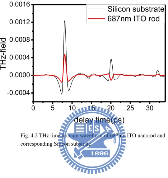
4.2 THz time domain waveform of 687nm ITO nanorod and corresponding Silicon substrate………. 50
4.3 THz time domain waveform of 536nm ITO nanorod and corresponding Silicon substrate………. 51
4.4 THz frequency domain spectra of 323nm ITO nanorod and corresponding Silicon substrate………. 52
4.5 THz frequency domain spectra of 722nm ITO nanorod and corresponding Silicon substrate………. 53
4.6 THz frequency domain spectra of 687nm ITO nanorod and corresponding Silicon substrate………. 54
4.7 THz frequency domain spectra of 536nm ITO nanorod and corresponding Silicon substrate………. 55
4.7.1 THz frequency domain spectra of 323nm ITO nanorod and corresponding Silicon substrate………. 56
4.7.2 THz-TDS waveform of four type of Silicon substrate……... 57
4.7.3 THz-TDS waveform of extension by the dash line of Fig. 4.7.2……... 57
4.7.4 THz frequency domain spectra of four Silicon substrate……….. 58
4.7.5 The real part of refractive index with four type of Silicon substrate…. 59 4.7.6 The image part of refractive index with four type of Silicon substrate. 60 4.8 The complex refractive index of 722nm ITO rod……….. 61
4.8.1 The complex refractive index of 687nm ITO rod……….. 62
4.10 The complex refractive index of 323nm ITO rod……….. 64 4.11 The complex refractive index respectively for 722nm, 687nm 536nm
and 323nm ITO nanorods……….. 65 4.12 The parameter r2 for fitting……… 66 4.13 Experimental complex conductivity and the fitting curve of 722nm
ITO rod………... 67
4.14 Experimental complex conductivity and the fitting curve of 687nm
ITO rod………... 68
4.15 Experimental complex conductivity and the fitting curve of 536nm
ITO rod………... 69
4.16 Experimental complex conductivity and the fitting curve of 323nm
ITO rod………... 70
4.17 The complex conductivity and fitting result respectively for 722nm,
687nm 536nm and 323nm ITO nanorods……… 71 4.18 Reflectivity spectrum of ITO nanorods in frequency domain………... 74 4.19 The fitting result of 722nm ITO nanorod with thickness of 722nm….. 75 4.20 Fitting results of 722nm ITO nanorod with thickness of 522nm……... 76 4.21 Fitting results of 722nm ITO nanorod with thickness of 322nm……... 77 4.22 Fitting results of 722nm ITO nanorod with thickness of 200nm……... 78 4.23 Fitting results of 722nm ITO nanorod with thickness of fitting
parameters of 722nm, 522nm, 322nm, 200nm……….. 79 4.24 Least Squares parameter with different thicknesses……….. 79
List of Tables
4.1.1 Fitting parameters of 722nm ITO rod……… 67
4.1.2 Fitting parameters of 687nm ITO rod……… 68
4.1.3 Fitting parameters of 536nm ITO rod……… 69
4.1.4 Fitting parameters of 323nm ITO rod……… 70
4.1.5 Fitting parameters respectively for 687nm , 722nm,536nm and 323nm ITO nanorods………..…………... 71
4.2 Electrical parameters of ITO nonorods for four thicknesses ITO nanorods…... 72
Chapter 1: Introduction
1.1 THz radiation
Terahertz radiation is type of electromagnetic waves at frequencies in the terahertz region and it referred to as the frequencies from 100 GHz to 30 THz. Terahertz lies in the frequency gap between the infrared and microwaves as shown in the Figure 1.1. 1 THz is equivalent to 33.33cm-1 (wave numbers), 4.1 meV photon energy, or 300 μm wavelength.
In the early time, people don’t know much about terahertz because the generation and detection technologies are not well established. At middle 1980s, the development of femtosecond laser contribute to the studies of terahertz and Auston successfully used photoconductive dipole antenna to generate and detect coherently THz radiation in time domain [1]. This technology is called terahertz time domain spectroscopy (THz-TDS). After the research of Auston, many other generation methods have been developed such as optical rectification [2], surge current in semiconductor surface [3], quantum cascade laser [4] and successfully used ZnTe crystal to detect THz radiation by free-space electro-optic sampling [5].
100 103 106 109 1012 1015 1018 1021
DC Kilo Mega Giga Tera Peta Exa Zetta
a
Yotta
Microwave Visible X-Ray λ-ray
Terahertz has much smaller photon energy (4.1 meV) compared to X-ray and therefore this kind of non-destruction measurement can be used for biology and medical sciences [6]. Image and tomography [7] of THz have also been studied and can be applied to homeland security.
1.2 Material of nanostructures
A nanostructure is an object of intermediate size between molecular and micrometer-sized structures. Performance of devices based on semiconductor nanomaterials can depend sensitively on the nanostructure morphology. Material of nanostructures include nanorod, nanoparticle, nanoshell, nanoring, nanocages[8], nanoflower[98], nanocomposite and nanoflake. Compare with a bulk, material of nanostructure usually have different optical and electrical properties. That is why people interesting in nanostructure materials.
Interest in nanotechnology is growing rapidly. Now it is possible to arrange atoms into structures that are only a few nanometers in size. A nanometer is about four atom diameters or 1 / 50000 of a human hair. A particularly attractive goal is the self-assembly of nanostructures, which produces large amounts of artificial materials with new properties.
Recently, many nanostructured semiconductors like InP-nanoparticle [10], ZnO-nanowire [11], Si-nanoparticle [12] have been studied using THz-TDS technology and the particular conduction behavior have been observed. In comparison with conventional far-IR source and detector, THz-TDS is a coherent technology that means both amplitude and phase information can be obtained.
1.3 Transparent Conductive Oxides (TCOs)
Materials that exhibit high optical transmittance and large electrical conductivity are of importance in many contemporary applications. An interesting group of materials with these properties is known as transparent conducting oxides (TCOs), with indium tin oxide (In2O3 : Sn,
denoted ITO) one of the most frequently investigated materials. It is used, for example, as an electrode in light emiting diodes [13] [14], solar cells [15], electrochromic devices such as smart windows, and flat panel displays.
1.4 Motivation for THz measurement
For the sample of nanorod, we can’t easily measure it by direct Hall measurement or four probe measurement. Because we are interesting in the electrical properties of individual nanorod structure. Although the direct four-probe electrical-transport measurement of nanowire had been reported [16], it is hard to do and contain some luck. By optical analysis we can easily measurement the nanostructure sample.
Comparing with conventional Hall measurement, THz-TDS is a non-contact method and it can avoid destroying the surface of nanostructure material. The electrical properties of nanostructure material can be derived from the experimental conductivity by fitting with the Drude model or Drude-Smith model.
Chapter 2: Experimental and theoretical
method
2.1 THz time-domain spectroscopy 2.1.1 THz time-domain spectroscopy
THz time-domain spectroscopy (THz-TDS) has been proven as an effective, noncontact method for determination of the electrical characteristics such as conductivity and mobility of materials. The setup of the transmittance THz system is discussed chapter 3. The temporal profile of THz signal can be mapped out by monitoring the bias crossing the electrode of the detection antenna from a lock-in amplifier as a function of delay time between the pump pulse and the probe pulse. Therefore, we can obtain the information for both amplitude and phase. In this section, we will discuss the experimental and theoretical method for THz-TDS in order to extract the optical and electrical properties of materials.
2.1.2 Propagation of electromagnetic wave
Thick samples
If the sample is thick enough, the main signal of transmission in time domain is clearly separated with reflection signal as shown in Fig.2.2. We used high resistivity Silicon wafer with thick of 525 micron meter as example. Thus, we can cut the reflection signal in order to simplify our analysis (dotted line).
Figure 2.1 show the ray optics method of the thick sample. The time delay can be equal to distance / c, c is the speed of light. Thus we can determine the delay of second reflection and third reflection signal as following: 6 8 2 2 525 10 12 / 3 10 / 3.42 thickness delay ps c n (2-1)
Compare with Fig.2.2 , we can find out the second signal in delay of 12ps after main signal and equal delay from second to third signal. Finally, the ray optics method seems more reasonable. If the sample is thick enough, the main signal of transmission in time domain is clearly separated with reflection signal. Thus, we can cut the reflection signal in order to simplify our analysis
Fig.2.1 Figure of ray optics model for thick sample Main signal
Second reflection signal
Third reflection signal
Thin samples
Considering a thin film Silicon with thickness below 50μm, the time delay will be smaller than 1 ps , which is in duration of THz pulse. We can not distinguish the second reflection from the main pulse. Thus, we consider the multi-beam reflection in our analysis.
Fig.2.3.1 and 2.3.2 show the basic diagrams of the light propagating through the sample and the reference. E0(ω) is the incident THz field,
Eref(ω) is the field after the light propagated from substrate, Esig(ω) is the
signal field transmitted through the sample. n1, n2 and n3 are the refractive
index for air, sample and substrate respectively. d is the thickness of sample and c is speed of light. The concept will be applied to the THz-TDS analysis with gathering both reference and signal data.
-5 0 5 10 15 20 25 30 35 -0.0004 0.0000 0.0004 0.0008 0.0012 THz -F iel d(a.u) time delay(ps) Main signal
Second reflection signal
Third reflection signal
Fig.2.2 THz time-domain waveform transmitted the 525m
Now, we consider the THz beam to normal incidence. From Fresnel equation, we know that amplitude transmission and reflection coefficient
d
D
Incident beam
Fig.2.3.2 The diagram of the sample
d
D
Incident beam
2 t i ij i j n n n (2-2) 2 t i ij i j n n n (2-3) j i ij i j n n r n n (2-4)
We can write down the reference and signal field in the form of , can be determined by 1 3 13 31 0 ( ) ( ) n d n D i c ref E t t E e (2-5)
By considering the multiple reflection within the thin sample, can be expressed by 3 31 ( ) ( ) n D i c sig sample E t E e (2-6) 2 2 2 2 3 0 12 23 0 12 23 21 23 5 (2 1) 2 2 0 12 23 21 23 0 12 23 21 23 ( ) ( ) ( ) ( ) ( ) n d n d i i c c sample n d q n d i i q q c c E E t t e E t t r r e E t t r r e E t t r r e (2-7)
where q is the number of multiple reflection, and assuming the number of multiple reflection is infinite(q ), Esample can be simplified as
2 2 12 23 0 2 12 23 ( ) 1 n d i c sample n d i c t t e E E r r e (2-8)
For n1 is the refraction index of air (n1=1) and t12t23t13r21r23 are
Fresnel amplitude transmission and reflection coefficient which can be represented by 12 2 2 1 t n 2 23 3 2 1 n t n 13 3 2 1 t n 2 21 2 1 1 n r n 2 3 23 2 3 n n r n n (3-9)
From equation (2-5) and (2-6), the theoretical complex transmittance can be given by 2 2 ( 1) 12 23 2 13 21 23 ( ) ( ) ( ) (1 ) n d i c sig the n d i ref c E t t e t E t r r e (2-10)
This formula is the theoretical complex transmittance of our thin sample, only if the substrate is thick enough. Otherwise, we should take the multi-beam reflection into account of the substrate. All the substrate we used is about 500μm, so it is clearly separated with reflection signal as shown in Fig.2.4.
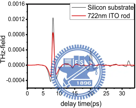
Fig.2.4 THz time-domain waveform transmitted the 323nm ITO rod on 525msilicon substrate.
0 5 10 15 20 25 30 -0.0004 0.0000 0.0004 0.0008 0.0012 THz -F iel d(a.u) time delay(ps)
On the other hand, we also can use ray optics method to determine the same transmittance. For tracing the beam, we take the reflectance and phase into condition as shown in Fig.2.5. k nd0 k is wavenumber, n is
refractive index of medium and d is traveling distance of the beam.
The total reflectance can be expressed by
1 1 1 1 2 2 2 4 12 23 12 12 23 21 12 23 21 21 2 12 23 ( ) ... 1 j j j j r r e r t r t e t r r t e r r e (2-11)
Because t=1+r, the transmittance can be determined by
1 1 1 1 2 12 23 12 23 2 2 12 23 12 23 (1 )(1 ) 1 1 j j j j r r e t t e t r r e r r e (2-12)
Finally, equation (2-12) is equal to (2-10). Two methods of calculate the transmittance can get the same formula, it shown this theoretical transmittance is reliable.
Fig.2.5 Three phase (air/sample/substrate) using multiple reflection to calculate the transmittance.
2.1.3 Refraction index extraction
We used Terahertz Time Domain Spectroscopy (THz-TDS) to determine the Experimental transmittance. By using the Fourier transform, the original time domain data is going to be the frequency domain. Figure 2.5.1 show the original transmittance of air and transformed to frequency domain. In frequency domain, we only used real part of transmittance in our calculation. We got the Experimental data for both sample and reference. Thus, we give the Experimental transmittance to . Obviously, it doesn’t exit an exact solution for the complex refractive index. So, we used a numerical method to extract the refractive index. In this way, we define an error function as below
exp( , 2, 2) the( , 2, 2) ( , 2, 2)
t n t n Error n (2-13)
First, we decided the frequency ω, if it exist the complex refractive index which makes the error function closest to zero. We can extract that refractive index by use of mathematical program.
2 2 [ ( , , )]
FindMinimum Error n (2-14)
We determine a range of complex refractive index for calculation and extract the best one which makes the error function is closest to zero for each frequency. Figure 2.6 is the contour plot of error function with ITO thin film. We set the range of complex refractive index of
position in the contour plot. With the program, we find the local minimum of 2D sets and gathering all of them in each frequency. Finally, we found the complex refractive index extracting from the experimental data. Figure 2.6.1 show the complex refractive index of ITO thin film in each frequency calculated with Wolfarm Mathematica for example.
0 10 20 30 40 50 60 -0.0005 0.0000 0.0005 0.0010 0.0015 TH z-Fie ld(a.u) delay(ps) -6 -4 -2 0 2 4 6 Pow er frequency(THz)
FFT
Fig.2.5.1 (a) Original transmittance of air in time domain (b) In frequency domain
(a)
Fig.2.6.1 Real part of refractive index (left) and image part (right) calculated in Wolfarm Mathematica for example.
Fig.2.6 The contour plot of error function for n, k 0.5 1.0 1.5 2.0 20 25 30 35 40 45 0.5 1.0 1.5 2.0 20 25 30 35 40
The following figure is the extraction of complex refractive index step by step. The complex refractive index is frequency dependence and the next section discuss how to determine the complex conductivity by the refractive index
【ω, n2, ,κ2】 【ω, n2, ,κ2】 THz TDS system Substrate (ref) Sample (sig) Experimental transmittance
Three phase Fresnel equation
Theoretical transmittance
Error【ω, n2, ,κ2】
Frequency dependence 【n2, ,κ2】
2.1.4 Optical conductivity Maxwell equation
Maxwell equations represent one of the most elegant and concise ways to state the fundamentals of electricity and magnetism. There are four partial differential equations that relate the electric and magnetic fields to their sources. Furthermore, these equation can be combined to show that light is an electromagnetic wave. Maxwell equation is shown as below:
D
Gauss’s law (2-15)
0
B
Gauss’s law for magnetism
(2-16) B E t Faraday’s law (2-17) D H J t
Ampere’s law with Maxwell
correction (2-18)
E: electric field B: magnetic field
D: electric displacement field
H: magnetizing field, also called magnetic field intensity
In our case, we separate bound charge and bound current from free charge and free current. It is more useful for calculation involving dielectric materials.
Complex dielectric function
First, we know the complex refractive of our sample from above calculation. Second, we can use the real and image part of refractive to calculate the complex conductivity. Third, we assumed a simple conducting medium with flowing current J E, then Maxwell equation
(2.18) can be shown as following:
0 0 0 0 0 [ ] D H J J i E t i E i E i i (2-19)
ε is the effective dielectric constant. We can determine effective dielectric constant from the refractive index by the relation as following:
2 ( ) r i i n i (2-20) 2 2 2 r i n n (2-21)
the complex conductivity can be obtained from equation (2-19)
0 0 0 ( ) ( ) ( ) ( ) r i r i i r i i (2-22)
Therefore, we obtained the experimental conductivity of real and image part from complex refractive index by equation (2-22). Fig.2.7
show that the complex refractive index determined the complex conductivity of experimental data.
Fig.2.7 Complex refractive index determined complex conductivity of 687nm ITO nanorod
0.5 1.0 1.5 0 10 20 30 40 50 refract ive index frequency(THz)
real part of refractive index real part of refractive index
0.5 1.0 1.5 -100 0 100 200 300 400 500
real part of conductivity image part of conductivity
C o n d u c ti v it y ( -1 cm -1 ) frequency(THz)
Drude free-electron model
The Drude free-electron model describes the dielectric function ε(ω) of a material, ε(ω)= [n(ω)+ik(ω)]2
, consisting of bound electrons and conduction band electrons in the THz region approximation is given by [17] 2 2 ( ) P i (2-23)
where the first term ε∞ is high-frequency dielectric constant contributed
from valence electrons (bound electron), the second term is from conduction electrons. ωP is the plasma frequency, ω is the angular
frequency, and τ is the electronic scattering time. The second term arises from the free carrier contribution where the characteristic plasma frequency ωP for the free carriers
2 2 * 0 C P e N m (2-24)
where NC is the free charge carrier concentration, and m* is the effective
free-electron mass, and e is the electron charge. The parameters ωP and τ
are obtained from fitting the THz data. The mobility μ =eτ /m*
can be found from the momentum relaxation time.
The dielectric function from equation (2-19) (2-20) and (2-23) can be written as:
2 2 2 2 0 ( ) N( ) n( ) ik( ) i = P i (2-25)where n(ω) and k(ω) are the frequency dependent real and imaginary parts of the complex refraction index N(ω). Therefore, we can obtain the complex conductivity from the Maxwell equation and the Drude free-electron model. The complex conductivity is denoted by
2 0 ( ) ( ) ( ) P r i i i i (2-26) where ε0=8.854×10 −12
(F/m) is the free-space permittivity. The real and imaginary parts of experiment conductivity σ(ω) are given by equation (2-22). For calculating the real and imaginary part of σ(ω) from equation (2-26), we know that 2 0 2 2 ( ) 1 P r (2-27) 2 0 2 2 ( ) 1 P i (2-28)
First, from transmittance terahertz time domain waveform we have the experimental complex refractive index by three-phase Fresnel equation (2-10). Second, the experimental complex refractive index can be transformed to complex conductivity by extended Maxwell equation (2-22). Third, the experimental complex conductivity by fitting with Drude free-electron model is shown in Figure 2.8. The scatter is the experimental conductivity and blue line is fitting result. Finally, by fitting the conductivity from Drude free-electron model (2-27) and (2-28), we determined the fitting parameter of plasma frequency ωP and scattering
time τ of our sample.
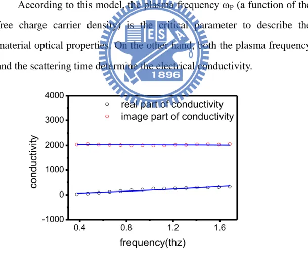
According to this model, the plasma frequency ωP (a function of the
free charge carrier density) is the critical parameter to describe the material optical properties. On the other hand, both the plasma frequency and the scattering time determine the electrical conductivity.
0.4 0.8 1.2 1.6 -1000 0 1000 2000 3000 4000
real part of conductivity image part of conductivity
conduct
ivi
ty
frequency(thz)
Fig. 2.8 The complex conductivity of 483nm ITO thin film. The red scatter is real part of conductivity and black scatter is image part of conductivity.
The following figure is the extraction of mobility and carrier concentration step by step. From the frequency dependence refractive index, we can determine the complex conductivity. By fitting the complex conductivity, we extract the fitting parameters and finally calculate the mobility and carrier concentration.
σr(ω) = 2nκωε0
σi(ω) =ωε0(ε∞-n2+κ2)
Drude model
σr ( ω,ωp,τ )
σi (ω, ,ωp,τ )
Fitting complex conductivity by ωp,τ
Fig.2.8.1 Mobility and concentration extraction step by step
Frequency dependence 【n2, ,κ2】
ωp carrier concentration
Drude smith model
While THz is widely used in Chemistry research and measurements of the conductivity of semiconductor, the flexibility Drude model have been invested in THz region. Better fits model are in the form of modified Lorentzians [18] 0 1 ( ) [1 (i ) ] (2-29)
where the exponents 1-α and β are treated as disposable parameters. With α=0 and β=1, we have the Drude result. With β=1 and α setting as variables is called the Cole-Cole(CC) model. With α=0 and varying the value of β, it is called the Cole-Davidson(CD) model.
The formula with Lorentzian form requires that the frequency dependent conductivity should have the maximum at the zero frequency and then fall off. Departure phenomena have been observed, and we have to concern with those materials in which σ(ω) displays a minimum at zero frequency and a transfer of oscillator strength to higher frequencies in the form of an impulse response.
The conduction properties of many semiconductors in the terahertz region have been justified to follow the simple Drude model, but some nanostructured materials show deviations from it. Recently, Smith proposed a modified Drude model [19], which can explain the deviations from the simple Drude model for the nanostuctured materials, particularly the negative values of imaginary part of conductivity. The complex
conductivity in the Drude-Smith model is given by 2 0 ( ) 1 1 1 p c i i (2-30)
This generalized Drude formula is called Drude-Smith model following the name of the inventor, Smith. Where c is a parameter describing fraction of the electron’s original velocity after scattering and vary between -1 and 1. In the simple Drude model, the momentum of carrier is randomized after each scattering event, but in the Drude-Smith model, carriers retain a fraction c, of their initial velocity. In particular, c = 0 corresponds to the simple Drude conductivity and c = –1 means that carrier undergoes complete backscattering.
Thus, the equation (2-26) can be modified, the theoretical complex conductivity is denoted by equation (2-30) in some nanostructured materials. By fitting the experimental complex conductivity with fitting parameters ωp , τ and c. The reduced dc conductivity in the Drude-Smith
model is given by σ=(1+c)eNμ. Therefore, a large negative value of c implies that electron backscattering occurs at the boundaries and surfaces of nanostructures and consequently suppresses dc conductivity. The reduce DC mobility is given by μ =(1+c)eτ /m*
.
Figure 2.8.2 and 2.8.3 show the complex conductivity of Indium nitride (InN) film and nanorod [20]. The complex conductivity response of the nanorods is different with InN film. The real part of conductivity gradually increases with increasing frequency, while image part with a negative value decreases with increasing frequency. This frequency dependence can’t be explained by the simple Drude model, in which the frequency-dependent conductivity has a maximum at zero frequency and
monotonically decreases with frequency. Using the Drude-Smith model, an excellent fit of complex conductivity of the InN nanorods is obtained.
Fig.2.8.3 [7] Conductivity of the InN nanorods. Solid and dashed lines correspond to the calculated results based on the Drude-Smith model.
Fig.2.8.2 [7] Conductivity of the InN film. Solid and dashed lines correspond to the calculated results based on the simple-Drude model.
2.2 Fourier transform infrared spectroscopy
2.2.1 Fourier transform infrared spectroscopy
Fourier transform infrared (FTIR) spectroscopy is a measurement technique that allows one to record infrared spectra. Infrared light is guided through an interferometer and then through the sample. A moving mirror inside the apparatus alters the distribution of infrared light that passes through the interferometer. The signal directly recorded, called an "interferogram", represents light output as a function of mirror position. A data-processing technique called Fourier transform turns this raw data into the desired result (the sample's spectrum): Light output as a function of infrared wavelength (or equivalently, wavenumber). As described above, the sample's spectrum is always compared to a reference. FTIR was used to investigate the optical properties of the materials in the near-IR spectral region. The reflectance or transmittance data were used to determine the plasma frequency and the electronic scattering time using the Drude free electron model or Drude-Smith model. The complex dielectric function of materials also determined. In this section, we will reveal how to derive the optical and electrical parameters by frequency dependence reflectance. At first, we should make the classification of the sample such as two-phase (air/sample) and three-phase (air/sample/substrate).
2.2.2 Complex dielectric function
We can determine the frequency dependence reflectance or transmittance by Fourier transform infrared (FTIR) spectroscopy [21]. By measuring
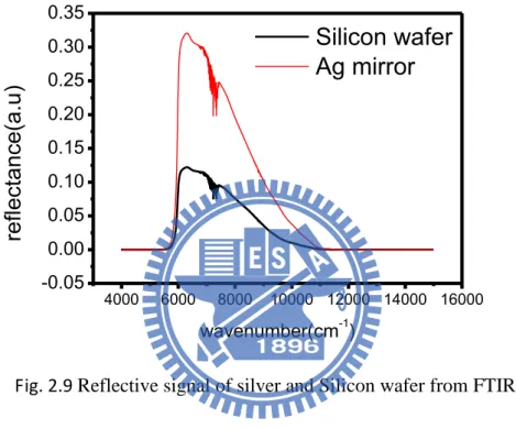
the reflectance signal or transmittance signal for both sample and background, frequency dependence reflectance or transmittance can be denoted. We usually use a 100% reflectance mirror such as gold surface or silver to be the background. Figure 2.9 is the reflective signal of silver and Silicon wafer in the range from 6000 cm-1 to 11000 cm-1.
The experiment reflectance can express as:
exp ( ) ( ) ( ) sample ref r r r (2-31)
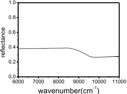
Finally, the experimental reflectance of Silicon wafer had been shown in Figure 2.10. We used Fourier transform infrared (FTIR) spectroscopy to determine the experimental reflectance. In the next section, we will extract the theoretical reflectance to calculate with the experimental reflectance. 4000 6000 8000 10000 12000 14000 16000 -0.05 0.00 0.05 0.10 0.15 0.20 0.25 0.30 0.35 refl ect ance(a.u ) wavenumber(cm-1) Silicon wafer Ag mirror
In order to determine the theoretical reflectance of the materials, we should make the classification of the sample such as two-phase (air/sample) and three-phase (air/sample/substrate) at first.
Sample of two-phase (air/sample)
The reflection of two-phase Fresnel equation in the beam of p-polarized can be expressed as following:
2 2 1 1 p 1 1 2 2 cos cos cos cos N N r N N (2-32)
Where θ1 is the angle of incident beam and θ2 is the refractive angle
determined by Snell’law. Snell’s law is a formula used to describe the
6000 7000 8000 9000 10000 11000 0.0 0.2 0.4 0.6 0.8 1.0 refl ect ance
wavenumber(cm
-1)
other waves passing through a boundary between two different isotropic media, such as water and glass. The law says that the ratio of the sines of the angles of incidence and of refraction is a constant that depends on the media. N is the complex refractive index of the material.
1sin 1 2sin 2
n n (2-33)
Sample of three-phase (air/sample/substrate)
The reflection of three-phase Fresnel equation in the beam of p-polarized can be expressed as following:
1 1 2 12 23 2 12 23 1 j p j r r e r r r e (2-34) 0 k nd
Equation (2-33) had been demonstrated is section 2.1, where r12 represent
the reflection coefficient from phase one to phase two which can determine by equation (2-32) . The power reflectivity for p-polarization is then shown as 2 p p R r (2-35) Optical conductivity
The Drude free-electron model describes the dielectric function ε(ω) of a material, ε(ω)=[n(ω)+ik(ω)]2
, consisting of bound electrons and conduction band electrons which is discussed in section 2.1.4. The complex dielectric function can be written as
2 2 ( ) P i (2-36)
Remember that: 2 2 * 0 C P e N m * e m (2-37)
Finally, we take the complex dielectric function (2-36) into the theoretical reflectance (2-32) (2-34) so the theoretical reflectance with the parameters of plasma frequency and scattering time can be extracted. Thus, we give the experimental reflectance to . So, we used a numerical method to extract the electrical parameters. In this way, we define an error function as below
2 exp ( p, ) [ the( p, , ) ( ) ]
error Sum R R (2-38)
In the summation of all frequencies, we make the error function to be the minimum with the electrical parameters:
[ ( p, )]
NMinimize Error (2-39)
Finally, the electrical parameters will be extracted by fitting the reflectance which measured from Fourier transform infrared (FTIR) spectroscopy.
determine the experimental reflectance. By fitting the reflectance, we finally extract the fitting parameters.
【ω , ωp , τ】
FTIR
Background (ref) Sample (sig)
Experimental reflectance
Two-phase Fresnel equation Three-phase Fresnel equation
Theoretical reflectance
Sum【│Rthe – Rexp│
2
】in all frequency
Error (ωp , τ)
Fig.2.11 Electrical parameters extract by FTIR step by step exp Sample R Background Rexp = Sample Background
Drude or Drude-smith model
ωp , τ
Chapter 3: Experimental setup
3.1 THz time domain spectroscopy 3.1.1 Ultrafast laser system
The progress in technology and applications in the field of ultrafast processes has been remarkable within the last two decades. The advent of all-solid-state femtosecond laser sources combined with highly efficient frequency conversion technique used for their wavelength extension has provided a variety of high performance sources for extremely short light pulses.
Here, we used the commercial oscillator titanium sapphire laser as the seed laser (Tsunami, Spectra-Physics). It is pumped by a frequency-doubled diode-pumped Nd:YLF laser at 532nm with the pump power of 4.2W. The titanium sapphire laser provides an output trace of intense 55fs pules with the wavelength from 750nm to 850nm, we adjust the center wavelength to about 800nm. The pulse repetition rate is approximately 90MHz and the output power is 500mW.
Figure 3.1 is the setup of Kerr-lens mode-lock (KLM) titanium sapphire ultrafast laser. The pump laser with the wavelength 532nm focus on titanium sapphire rod by the lens (L1) and stimulated the fluorescence
with the wavelength of 800nm. The fluorescence has been collected by two concave mirror (R1,R2) with high reflection in 800nm and
anti-reflection in 532nm. Then, we input the prism pair in a arm with high reflection mirror R5 in order to compensate the dispersion. Finally, we
used the output coupler R4 to finish the setup of resonant cavity on the other arm. R5 R1 R4 R1 λ / 2 plate Pump Laser Output Coupler Ti:sapphire rod
Fig.3.1 The setup of Kerr-lens mode-lock (KLM) titanium sapphire ultrafast laser.
3.1.2 THz time domain spectroscopy (transmittance) Delay stage Emitter BS Detector Sample Lockin Amplifier Stage Controller Function Generator
Pulse width: 55 fs
Repetition rate: 90 MHz
Wavelength: 800nm
Pump/Probe power: 30mW/20mW
Emitter/Detector: LT-GaAs
The schematic of the transmittance THz system is shown in Figure 3.2.1. A oscillator Ti:sapphire laser with center wavelength of 800nm at repetition of 90MHz is used and the pulse duration is 55fs.
First, the femtosecond laser beam is divided by a beam splitter. One
Laser excitation
Electrode
Semiconductor substrate
Silicon lens
5μ m
is pump beam and the other is probe beam. The pump beam is focused on the photoconductive antenna by objective lens. A 5volt AC bias with frequency of 1KHz is applied to the emitter antenna to accelerate the carriers excited by the pump pulse by a function generator. Then, the terahertz ray radiated from photoconductive antenna and we used a parabolic mirror to collect the THz beam. We focus the THz beam on the sample and collect the transmittance beam by another parabolic mirror. Finally, we also focus the transmittance THz beam on the detector which contact with the lock-in Amplifier. Second, the probe beam path through the delay stage is used to adjust the delay compare with the pump beam. The probe beam finally go into the antenna detector. By using the controller to make the different delay of pump beam and probe beam, we can record the signal as a function of delay by the lock-in amplifier. Figure 3.2.3 show the THz time domain waveform of air with one step of delay in 10micrometer and total of 512 steps. The corresponding power spectrum is also as shown. In time domain waveform, we can see there are still many noises after main signal and their corresponding power spectrum show many absorption peaks. This is contributed to the water vapor absorption [22]. Water is almost perfectly transparent to visible light but great absorption in THz region which is shown in Figure 3.3.
In order to avoid water vapor absorption, the entire THz beam is located in a closed acrylic box which is purged with nitrogen gas to decrease the water vapor. At purged about 30minutes, the environmental humidity decrease from about 60% to under 5%. The Thz time-domain waveform and their corresponding power spectrum under the humidity of
0.0 0.5 1.0 1.5 2.0 2.5 3.0 3.5 4.0 4.5 1E-16 1E-15 1E-14 1E-13 1E-12 1E-11 1E-10 1E-9 1E-8 Pow er as M SA frequency(THz) 0 5 10 15 20 25 30 35 -0.0005 0.0000 0.0005 0.0010 0.0015 E-f iel d time delay
Fig.3.2.3 THz (a)time-domain waveform (b)corresponding power spectrum in the air
about 5% are shown in Figure 3.4. From this figure, the time-domain waveform become smoother than before and the peak value of signal is larger. The absorption peaks in power spectrum also disappear and seem a useful range from 0.2 to 3THz in the air with low humidity.
Fig.3.3 The visible and UV spectra of liquid water (http://www1.lsbu.ac.uk/water/vibrat.html#comp)
0 5 10 15 20 25 30 35 -0.0005 0.0000 0.0005 0.0010 0.0015 E-f iel d time delay 0.0 0.5 1.0 1.5 2.0 2.5 3.0 3.5 4.0 4.5 1E-16 1E-15 1E-14 1E-13 1E-12 1E-11 1E-10 1E-9 1E-8 Pow er as M SA frequency(THz)
Fig.3.4 THz (a)time-domain waveform (b)corresponding power spectrum in the air with humidity under 5%
3.2 Fourier transform infrared spectroscopy
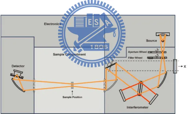
(The Fourier Transform Infrared Spectrometer : VERTEX 70v)
Infrared light emitted from a source is directed into an interferometer, which modulates the light. After the interferometer the light passes through the sample compartment (and also the sample) and is then focused onto the detector. The signal measured by the detector is called the interferogram.
3.3 Sample preparation
3.3.1 ITO nanorod (from Prof. Yu Peichen)
ITO nanoculumn is grown under the following conditions: 1. Deposition angle=700
2. Vacuum pressure=10-4 torr
3. ITO growth on high resistivity silicon substrate 4. Substrate temperature=240oC
5. With nitrogen flux
6. Using the commercial target composition is 95 wt% In2O3 + 5 wt%
SnO2
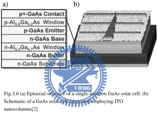
Figure 3.6 shows the epitaxial structure of a conventional, single-junction GaAs/AlGaAs solar cell[23]. After the standard fabrication process, the ITO-nanocolumn structure was deposited onto the p-type Al0.8Ga0.2As window layer using glancing-angle e-beam deposition,
followed by a post annealing process at 3500C for 25 minutes to improve the transmittance. The fabricated device is schematically illustrated in right of Figure 3.6 Glancing-angle deposition has been employed for preparing microscale and nanoscale porous materials based on nucleation formation and self shadowing effect. However, the characteristic ITO nanocolumn structure seen in this work is rather unique, where the formation involves either catalyst-free or self-catalyzed
vapor–liquid–solid (VLS) growth assisted by the introduced nitrogen. The substrate is tilted at a deposition angle of 700 with respect to the incident vapor flux, where the chamber pressure is controlled at 1.33 10-2 Pa [2].
Figure 3.7.1 is the picture of chamber taken from camera and Figure 3.7.2 is schematic drawing of chamber:
Fig.3.6 (a) Epitaxial structure of a single-junction GaAs solar cell. (b) Schematic of a GaAs solar cell fabricated employing ITO
nanocolumns[2]
C H A M B E R
ψ Holder ITO rod Vacuum Pump θ Normal LineFig.3.7.2 View of the chamber Fig 3.7.1 The picture of chamber
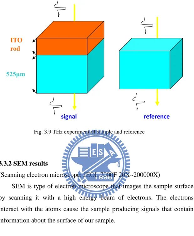
The substrate we used is high resistivity Silicon wafer. With the higher resistivity, the absorption of substrate will become lower. Figure 3.8 show the position of ITO rod grown on Silicon wafer. In section 2.2, we need the reference to determine the properties of sample. Here, the corresponding reference is on the Neighbor side of the sample. It make sure that the reference we used is approximatively same to the substrate of ITO rod.
Figure 3.9 shown the optical beam transmit the sample and reference. In calculation of section 2.2, the reference require approximatively same to the substrate of sample. Because the Silicon wafer is very thick compare with ITO nanorod, this phenomenon plays an important role in our experiment.
Ref(722nm)
536nm
323nm
ITO rod grown on here
525μm
High resistivity Silicon wafer
Fig.3.8 ITO rod grown on Silicon wafer 687nm
722nm
Ref(687nm)
Ref(536nm)
3.3.2 SEM results
(Scanning electron microscope: JEOL 7000F 20X~200000X)
SEM is type of electron microscope that images the sample surface by scanning it with a high energy beam of electrons. The electrons interact with the atoms cause the sample producing signals that contain information about the surface of our sample.
SEM image of sample
Substrate: 525μm high resistance Silicon substrate Four different thickness of ITO rod
Condition on (kÅ ) Height(nm)
1 2.4 687
2 1.8 722
3 1.2 536
4 0.6 323
Fig. 3.9 THz experiment of sample and reference
ITO rod
525μm
Figure 3.10 is the cross-sectional view with ×30000 enlargement and determined the thickness of 687nm. Figure 3.11 is top view of ITO nanorod with ×20000 enlargement.
Fig.3.11 687nm ITO nanocolumns with top view of SEM Fig.3.10 687nm ITO nanocolumns with cross-sectional view of SEM
Figure 3.12 is the cross-sectional view with ×20000 enlargement and determined the thickness of 722nm. Figure 3.13 is top view of ITO nanorod with ×22000 enlargement.
Fig.3.13 722nm ITO nanocolumns with top view of SEM Fig.3.12 722nm ITO nanocolumns with cross-sectional view of SEM
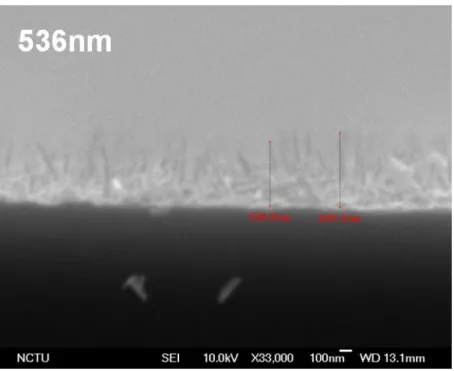
Figure 3.14 is the cross-sectional view with ×33000 enlargement and determined the thickness of 536nm. Figure 3.15 is top view of ITO nanorod with ×20000 enlargement.
Fig.3.15 536nm ITO nanocolumns with top view of SEM Fig.3.14 536nm ITO nanocolumns with cross-sectional view of SEM
Figure 3.16 is the cross-sectional view with ×33000 enlargement and determined the thickness of 323nm. Figure 3.17 is top view of ITO nanorod with ×20000 enlargement.
Fig.3.17 323nm ITO nanocolumns with top view of SEM Fig.3.16 323nm ITO nanocolumns with cross-sectional view of SEM
Chapter 4: Results and discussion
4.1 Extraction of complex refractive index 4.1.1 THz field in time-domain
722nm ITO rod : THz time domain waveform
Figure 4.1 is THz time domain waveform of 722nm ITO nanorod and corresponding high resistance Silicon substrate with 10μm one step of delay and total 512 steps. The lower one is the signal of ITO nanorod and higher one is the reference of substrate. In this figure, the peak positions are almost the same because that the ITO nanorod is too thin to distinguish the signal peak position and reference peak position. On the other hand, the reduction of peak value contribute to the absorption of
0
5
10
15
20
25
30
-0.0004
0.0000
0.0004
0.0008
0.0012
0.0016
TH
z-fi
el
d
delay time(ps)
Silicon substrate
722nm ITO rod
Fig. 4.1 THz time domain waveform of 722nm ITO nanorod and corresponding Silicon substrate
687nm ITO rod : THz time domain waveform
Figure 4.2 is THz time domain waveform of 722nm ITO nanorod and corresponding high resistance Silicon substrate with 10μm one step of delay and total 512 steps. The lower one is the signal of ITO nanorod and higher one is the reference of substrate. In this figure, the peak positions are almost the same because that the ITO nanorod is too thin to distinguish the signal peak position and reference peak position. Compare with Figure 4.1, the absorption of the 687nm ITO nanorod is larger than 722nm ITO nanorod. This phenomenon will discuss later.
0 5 10 15 20 25 30 -0.0004 0.0000 0.0004 0.0008 0.0012 0.0016
TH
z-fi
el
d
delay time(ps)
Silicon substrate
687nm ITO rod
Fig. 4.2 THz time domain waveform of 687nm ITO nanorod and corresponding Silicon substrate
536nm ITO rod : THz time domain waveform
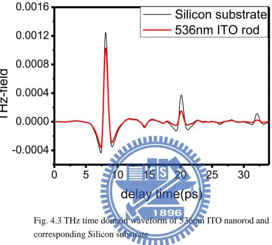
Figure 4.3 is THz time domain waveform of 536nm ITO nanorod and corresponding high resistance Silicon substrate with also10μm one step of delay and total 512 steps. The lower one is the signal of ITO nanorod and higher one is the reference of substrate. In this figure, the peak positions are almost the same because that the ITO nanorod is very thin. On the other hand, the reduced of peak value contribute to the absorption of ITO nanorod. Compare with the thicker sample, the absorption of 536nm ITO nanorod is smaller.
Fig. 4.3 THz time domain waveform of 536nm ITO nanorod and corresponding Silicon substrate
0 5 10 15 20 25 30 -0.0004 0.0000 0.0004 0.0008 0.0012 0.0016
TH
z-fi
el
d
delay time(ps)
Silicon substrate
536nm ITO rod
536nm ITO rod : THz time domain waveform
Figure 4.4 is THz time domain waveform of 536nm ITO nanorod and corresponding high resistance Silicon substrate with also10μm one step of delay and total 512 steps. The lower one is the signal of ITO nanorod and higher one is the reference of substrate. In this figure, the peak signal of ITO nanorod and the reference is very close, because the sample is thin enough so the absorption from the sample is not obvious to see.
Fig. 4.4 THz time domain waveform of 323nm ITO nanorod and corresponding Silicon substrate
0 5 10 15 20 25 30 -0.0004 0.0000 0.0004 0.0008 0.0012 0.0016
TH
z-fi
el
d
delay time(ps)
Silicon substrate
323nm ITO rod
4.1.2 THz spectrum in frequency domain
722nm ITO rod : In frequency domain
Figure 4.5 is THz frequency domain spectra of 722nm ITO nanorod and corresponding high resistance Silicon substrate. The lower one is the signal of ITO nanorod and higher one is the reference of substrate. It shown the reliable range from about 0.2 THz to 2 THz. Because our experiment is measured with the nitrogen purge, the humidity is under 5 % so the water absorption line almost disappeared. It let our analysis to be more convinced. Form section 2.1.3, the experimental transmittance of sample and reference can extract the complex refractive index.
0.0 0.5 1.0 1.5 2.0 1E-13 1E-12 1E-11 1E-10 1E-9 1E-8 1E-7
pow
er
frequency(THz)
Silicon substrate
722nm ITO rod
Fig. 4.5 THz frequency domain spectra of 722nm ITO nanorod and corresponding Silicon substrate
687nm ITO rod : In frequency domain
Figure 4.6 is THz frequency domain spectra of 687nm ITO nanorod and corresponding high resistance Silicon substrate. The lower one is the signal of ITO nanorod and higher one is the reference of substrate. It shown the reliable range from about 0.2 THz to 2 THz. With the frequency domain spectra of sample and reference, we can calculate the experimental transmittance. Form section 2.1.3, the experimental transmittance of sample and reference can extract the complex refractive index. 0.0 0.5 1.0 1.5 2.0 1E-13 1E-12 1E-11 1E-10 1E-9 1E-8 1E-7
pow
er
frequency(THz)
Silicon substrate
687nm ITO rod
Fig. 4.6 THz frequency domain spectra of 687nm ITO nanorod and corresponding Silicon substrate
536nm ITO rod : In frequency domain
Figure 4.7 is THz frequency domain spectra of 536nm ITO nanorod and corresponding high resistance Silicon substrate. The lower one is the signal of ITO nanorod and higher one is the reference of substrate. It shown the reliable range from about 0.2 THz to 2 THz and low absorption compare with Fig. 4.5 and Fig. 4.6. With the frequency domain spectra of sample and reference, we can calculate the experimental transmittance. Form section 2.1.3, the experimental transmittance of sample and reference can extract the complex refractive index.
0.0 0.5 1.0 1.5 2.0 1E-13 1E-12 1E-11 1E-10 1E-9 1E-8 1E-7
pow
er
frequency(THz)
Silicon substrate
536nm ITO rod
Fig. 4.7 THz frequency domain spectra of 536nm ITO nanorod and corresponding Silicon substrate
323nm ITO rod : In frequency domain
Figure 4.7.1 is THz frequency domain spectra of 323nm ITO nanorod and corresponding high resistance Silicon substrate. The lower one is the signal of ITO nanorod and higher one is the reference of substrate. It shown the reliable range from about 0.2 THz to 1.5 THz and the very small absorption compare with the reference. By improving the S/N ratio, we still can get the reliable data. With the frequency domain spectra of sample and reference, we can extract the complex refractive index from section 2.1.3.
0.0 0.5 1.0 1.5 2.0 1E-13 1E-12 1E-11 1E-10 1E-9 1E-8 1E-7
pow
er
frequency(THz)
Silicon substrate
323nm ITO rod
Fig. 4.7.1 THz frequency domain spectra of 323nm ITO nanorod and corresponding Silicon substrate
4.1.3 Optical constants of substrate
Optical constants of high resistivity Silicon substrate:525μm
From the THz-TDS waveform, four substrate of Silicon wafer have
0 10 20 30 -0.0010 -0.0005 0.0000 0.0005 0.0010 0.0015 0.0020 TH z-fi el d time delay(ps) air Silicon sub(722nm) Silicon sub(687nm) Silicon sub(536nm) Silicon sub(323nm) 8.0 8.2 8.4 0.00123 0.00126 0.00129 TH z-fi el d time delay(ps) air Silicon sub(722nm) Silicon sub(687nm) Silicon sub(536nm) Silicon sub(323nm) Fig.4.7.2 THz-TDS waveform of four type of Silicon substrate
Fig.4.7.3 THz-TDS waveform of extension by the dash line of Fig. 4.7.2
substrates are very close, because of all these substrates are cut from the same wafer. In the below, we will calculate the transmittance of ITO rod so we should make sure the reference we used is reliable.
The time domain waveform transform to frequency domain by Fourier transform. By the signal of Silicon substrate and reference of air, we calculate the complex refractive index from section 2.1.3. Thus, we got the results as following:
0
1
2
3
1E-8 1E-7 1E-6 1E-5 1E-4 1E-3am
pl
itude(a.u
.)
frequency(THz)
air Silicon sub(722nm) Silicon sub(687nm) Silicon sub(536nm) Silicon sub(323nm)Real part of refractive index by Silicon substrate
From the real part of refractive index of Fig.4.7.5, four type of Silicon substrate have similar value of refractive index. It shown that in the frequency range from 0.2THz to 2.5THz, the value of n are very close. We determined the value to be a constant of 3.42 as the reference. In the below, we use this constant to calculate the theoretical transmittance of ITO nanorods. 0.5 1.0 1.5 2.0 3.0 3.2 3.4 3.6 3.8 4.0
refract
ive
index
frequency(THz)
Fig.4.7.5 The real part of refractive index with four type of Silicon substrate
Image part of refractive index by Silicon substrate
From the image part of refractive index of Fig.4.7.6, the value of extinction coefficient close to zero because of low absorption of High resistivity Silicon. As the resistivity become larger, the conductivity will become smaller and indicate low absorption of terahertz .We assume the extinction coefficient to be zero in the below analyze of theoretical transmittance calculation. 0.5 1.0 1.5 2.0 -0.4 -0.2 0.0 0.2 0.4
ext
inct
ion
coef
fici
ent
frequency(THz)
Fig.4.7.6 The image part of refractive index with four type of Silicon substrate
4.1.4 Complex refractive index of ITO nanorods
722nm ITO rod : complex refractive index
We obtained 722nm ITO rod real and image part of refractive in the range from 0.2 THz to 1.6 THz. Noises cause the vibration of our data. The value of image part is larger than real part of refractive index.
0.2 0.4 0.6 0.8 1.0 1.2 1.4 1.6 0 5 10 15 20 25 30 35 40
com
pl
ex
refrat
ive
index
frequency(THz)
k
n
722nm ITO-rod
687nm ITO rod : complex refractive index
We have shown 687nm ITO rod real and image part of refractive in the range from 0.2 THz to 1.6 THz. But the vibration in the range from 1THz to 1.6 THz seems too large so that we guess the reliable range is from 0.2 THz to 1 THz. In the below, we will discuss how to determine to reliable range of our data. The value of image part is larger than real part of refractive index. 0.2 0.4 0.6 0.8 1.0 1.2 1.4 1.6 0 10 20 30 40