國 立 交 通 大 學
電子工程學系 電子研究所
碩 士 論 文
砷化銦量子點載子動力學之溫度相依性
Temperature-Dependent Carrier Dynamics of
InAs/GaAs Quantum Dots
研 究 生:鄭 濬
指導教授:林聖迪 博士
砷化銦量子點載子動力學之溫度相依性
Temperature-Dependent Carrier Dynamics of
InAs/GaAs Quantum Dots
研 究 生:鄭 濬 Student: Chun Cheng
指導教授:林聖迪 博士 Adviser: Dr. Sheng-Di Lin
國 立 交 通 大 學
電 子 工 程 學 系 電 子 研 究 所
碩 士 論 文
A Thesis
Submitted to Department of Electronics Engineering and Institute of
Electronics
College of Electrical and Computer Engineering
National Chiao Tung University
in Partial Fulfillment of the Requirements for Degree of Master in
Electronics Engineering
July 2011
砷化銦量子點載子動力學之溫度相依性
學生:鄭 濬 指導教授:林聖迪 博士
國立交通大學
電子工程學系電子研究所碩士班
摘 要
本論文探討成長於砷化鎵基板上之砷化銦量子點中,載子動態行
為對溫度的相依性。依據量測變溫的時間解析光譜,在一個小範圍的
溫度區間,隨著溫度升高,我們觀察到某些樣品中的光譜從兩段轉變
成單一指數衰減的特殊現象,擬合的載子生命期則在某個溫度劇烈的
變長爾後又隨著溫度再升高而下降。透過包含了暗能態之三能態速率
方程式模擬,我們推測在低溫時,載子被暗能態緩慢的態鬆弛時間所
限制而使光譜呈現兩段指數衰減;當溫度升高,額外且速率快的路徑
主導了載子傳輸使暗激子快速鬆弛並發光,此時光譜的行為呈現單一
指數衰減。此現象說明了欲高溫操作自旋儲存之相關元件,我們必須
考慮在高溫時載子藉由額外路徑被快速消耗的機制。
Temperature-Dependent Carrier Dynamics of InAs/GaAs Quantum Dots
Student: Chun Cheng
Adviser: Dr. Sheng-Di Lin
Department of Electronics Engineering & Institute of Electronics
National Chiao Tung University
Abstract
This work focuses on the temperature-dependent carrier dynamics of
InAs/GaAs quantum dots. We present an abnormal observation of
low-temperature spike on carrier lifetimes caused by the change of decay
curves from bi-exponential to mono-exponential decay. Theoretically, we
then propose a three-level system containing a dark excitonic state and
calculate it with rate equations; we find that at low temperature, the
curves behave bi-exponentially due to the slow rate of the spin-flip
relaxation of dark excitons; however at higher temperature, carriers are
able to relax through an additional path with a much faster rate and the
process becomes dominating, leading to the mono-exponential decay
curves. The study suggests that to realize high-temperature operation spin
storage taking the advantage of dark excitons in QDs, one must consider
the fast relaxation through the extra mechanisms favored by thermal
energy.
誌 謝
在交大的六年,日子不算短暫,如今即將要在我碩士班畢業畫下一個句點。 首先我非常感謝我的指導老師林聖迪老師的指導,在他的帶領下,不管是在學術 抑或是做事的方法上,兩年的碩士生涯讓我學到了很多;此外我所待的研究團隊 裡,三個指導老師、豐富的資源,還有實力堅強的學長姐,讓我所得到的訓練非 常紮實,也很珍惜待在這裡的每一刻。我要特別感謝幾位學長,建宏、大鈞、 KB 和小傅,有機會與你們一起共事是很榮幸的,我們總能在討論之中互相學習, 我受益良多;我也要謝謝我同屆的好同學們,雖然我們的研究題目是如此的不同, 但在平時的生活上,也因為有了你們而增添了許多歡笑及趣事,這將會是我之後 點滴的美好回憶。 除了電子研究所帶給我的許多,我要特別提及我大學所就讀的電子物理學系; 它帶給了我很好的訓練,讓我在之後研究的學問和方法上能夠很快地上軌道,這 是唯有把事情完成後才能深刻體會到的無形力量。謝謝曾經在我大學照顧和指點 過我的老師們,我會永遠記得你們。 最後把我的心血獻給我最親愛的父母親和所有的家人,唯有你們在這六年全 力的支持,才能夠讓我完成在交大的兩個學位,為之後的更多挑戰做好準備。我 由衷的感謝你們的照顧與付出,這是我一生中最大的福氣。我會繼續努力,多看 多做,期許自己更上層樓。Contents
中文摘要... i ABSTRACT ... ii 誌謝... iii CONTENTS... iv LIST OF FIGURES ... vi LIST OF TABLES ... ix CHAPTER 1 INTRODUCTION ... 1 1.1 A Brief Review ... 11.2 Motive – the Temperature Effect ... 4
CHAPTER 2 SPECTROSCOPY... 1
2.1 Carrier Dynamics in Semiconductor QDs ... 5
2.2 Steady-State Photoluminescence (SSPL) ... 6
2.3 Steady-State Photoluminescence Excitation (SSPLE) ... 7
2.4 Time-Resolved Photoluminescence (TRPL) ... 8
2.5 Experimental Setup in this Work ... 12
2.6 Fabrication of InAs QDs Samples ... 15
3.2.1 Observation and comparison ... 25
3.2.2 Energy-dependent TRPL ... 27
3.2.3 Power-dependent TRPL ... 28
3.2.4 Decay curves of PL intensity ... 29
3.3 The Prolonged Rising Time ... 32
3.4 Size Dependence of QDs on the Low-Temperature Spike... 32
3.5 Issues about the Sizes of QDs ... 37
CHAPTER 4 SIMULATION AND COMPREHENSION ... 38
4.1 Dark, Bright and Hot States (Excitons) ... 38
4.2 Rate Equations ... 41
4.3 Simulation Results ... 43
4.4 Mechanisms – the Effect of Temperature ... 46
4.4.1 Main discussion ... 46
4.4.2 Discussion on the influences of parameters ... 50
4.5 Additional Discussions ... 55
4.6 Issues and Limitation ... 56
CHAPTER 5 CONCLUSIONS AND FUTURE STUDIES ... 57
BIBLIGRAPHY ... 59
List of Figures
Chapter 1
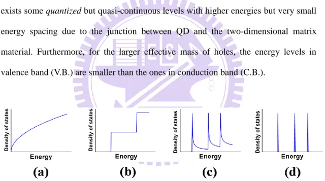
Figure 1-1: Density of states of (a) bulk, (b) QWs, (c) QWires and (d) QDs. ... 2
Figure1-2: Typical morphology on QD structures... 2
Figure 1-3: Schematic plots of energy levels in the QD system ... 3
Chapter 2
Figure 2-1: Typical procedures for carrier transitions in semiconductor QDs ... 6Figure 2-2: Schematic plot of the principle of PL generation. ... 7
Figure 2-3: Main principle of the pump-probe technique ... 9
Figure 2-4: Main principle of the steak camera technique ... 10
Figure 2-5: Main principle of the TCSPC technique ... 11
Figure 2-6: Final statistical integration of signal in the TCSPC technique ... 11
Figure 2-7: Schematic plot of the steady-state PL and time-resolved PL system ... 12
Figure 2-8: Final signal processing of the TRPL measurement. ... 14
Figure 2-9: Schematic plot of the Stranski-Keastanov mode formation... 16
Figure 2-10: Comparison of the effective eigenenergies of (a) free particle in a box and (b) QDs. ... 17
Figure 2-11: Structure of the InAs QDs studied in this work ... 18
Chapter 3
Figure 3-1: SSPL spectra @ T = 25 K of the six samples ... 21 Figure 3-2: SSPLE spectra @ T = 77 K of the four selective samples ... 22 Figure 3-3: (a) Carrier lifetime (τ1) and (b) PL intensity and FWHM of sample A .... 24
Figure 3-4: (a) Observation of low-T spike phenomenon in sample C; a typical result is shown in Sample A for comparison. (b) Corresponding integrated PL intensity and FWHM for both two samples ... 26 Figure 3-5: Energy-dependent TRPL measurement of sample A and C ... 27 Figure 3-6: Power-dependent TRPL of Sample C ... 28 Figure 3-7: Measured decay curves under excitation power of 2 μW for (a) Sample A and (b) Sample C with their corresponding carrier lifetimes (τ1) ... 30
Figure 3-8:Parameters evaluated from numerical fitting for (a) Sample A and (b) Sample C; (c): comparison of A2 ratio of sample A and C ... 31
Figure 3-9: Rising parts of (a) Sample A and (b) Sample C ... 32 Figure 3-10: T-dependent carrier lifetimes (τ1) for all six samples under 10 μW ... 33
Figure 3-11: Measured decay curves of (a) Sample B (b) Sample D (c) Sample E and (d) Sample F with their corresponding τ1 in the inset figures ... 34
Figure 3-12: Fitting parameters of all six samples. (a) to (d): τ1, τ2 of sample B, D, E
and F, respectively; (e): A2 ratio of all six samples ... 36
Figure 3-13: (a) SSPL spectra for sample B and C (b) corresponding τ1 at different
temperatures ... 37
Figure 4-2: Spin alignments of different kinds of excitons. ... 39
Figure 4-3: Flow chart of the simulation procedures ... 42
Figure 4-4: Comparison of (a) τ1 and (b) τ2 with simulation and experiment ... 43
Figure 4-5: Decay curves obtained from simulation... 44
Figure 4-6: A2 ratio at different temperatures with the corresponding τ1 ... 44
Figure 4-7: Carrier dynamics at low and high temperatures ... 46
Figure 4-8: τeff as a function of temperature ... 48
Figure 4-9: Simplified model with the new introduced parameter
τ
eff ... 49Figure 4-10: Discussions of the parameters: (a) relaxation time from hot to dark state (τhd) and hot to ground state (τhg); (b) spin-flip lifetime (τspin-flip) ... 51
Figure 4-11: Discussion of the parameters of energy spacing between: (a) hot and dark states (Δhd); (b) ground and dark states (Δgd) ... 52
Figure 4-12: The influence of initial portion of carriers at ground state ... 53
List of Tables
Table 2-1: Information of the InAs QDs samples ... 19 Table 3-1: List of peak energies and FWHM of the six samples ... 19 Table 3-2: List of parameters used for the calculation of injected e-h pairs ... 23
Chapter 1
Introduction
1.1 A Brief Review
Undoubtedly, III-V semiconductor materials set a decisive milestone in the development of applied photonics in the last few decades. Being very different from single-element semiconductors like silicon and germanium, the direct-bandgap property offers III-V semiconductors a substantial advantage on fabricating optoelectronic devices, bringing about a revolutionary change in our modern society. With the attractive features of ultra-small size and fine output efficiency, commercial products containing semiconductor lasers, light emitting diodes and other related devices are ubiquitous in our daily lives. Moreover, because of the wide variety choices on compound composition, application of higher extent has also been achieved in particular proposes such as infra-photodetectors for thermal imaging [1-4], mid-infrared semiconductor laser for gas detection [5-7], and even high efficiency solar cells [8-11]. In the future, to seek for new inventions and improvement of devices will certainly be one of the most definite targets.
In pursuit of better device performance, researchers have put effort on various emphases including the fundamental improvement on crystal quality and engineering on device structure. Recently, nano-scale structures such as quantum wells (QWs), quantum wires (QWires) and quantum dots (QDs) have intrigued scientists a lot; it is believed that the low-dimensionality of these structures can provide a better carrier
Fig. 1.1 shows the comparison of density of states (DOS) of bulk, QWs, QWires and QDs. The zero-dimensionality of QDs leads to a δ-like DOS [12], meaning both electrons and holes are spatially restricted in all dimensions and have only particular allowed states to occupy. Therefore, the property is exactly suitable for optoelectronic devices and researchers have worked greatly on this candidate structure.
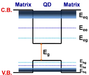
To conceptually introduce the QD system, we show a typical morphology on QD ensembles in Fig. 1-2, and the discrete-energy levels in QDs are also schematically plotted in Fig. 1-3; notice that the meanings of the symbols are mentioned in the figure caption. In addition to the relatively lower ground and excited states, there exists some quantized but quasi-continuous levels with higher energies but very small energy spacing due to the junction between QD and the two-dimensional matrix material. Furthermore, for the larger effective mass of holes, the energy levels in valence band (V.B.) are smaller than the ones in conduction band (C.B.).
Figure 1-3: Schematic plots of energy levels in the QD system. Symbols: Eg: bandgap
energy; Ee(h)g: ground state energy of electron (hole); Ee(h)e: excited state energy of
electron (hole); Ee(h)q: qausi-continuous state energy of electron (hole).
Within many QDs with different materials, In(Ga)As QDs are so attractive due to the benefit on easy fabrication on matured-studied GaAs system. There are many demonstrations about the great characteristics of InAs QD-based devices such as the lower threshold current of laser diodes [13-15] and higher operation temperature of infrared photodetectors [1, 2]; also, it provides a great opportunity for tuning the emission wavelength to telecommunication range [16]. On the other hand, it has been shown that InAs QDs can be used as devices of quantum photonics like single photon emitters, being a tempting choice for the use of quantum information processing [17-19].
1.2 Motive – The Temperature Effect
In order to further realize the room temperature operation for advanced QD-based devices, an indispensible work of understanding the temperature effect on the QD systems turns out to be necessary. As non-zero thermal energy being naturally inventible, we must factor in its influence as considering both the device performance and reliability; it is especially more crucial for devices fabricated with quantum structures since the related energy of the systems is often in the order of eV, or even smaller to be meV; therefore, the investigation of temperature effect remains one of the most valuable topics in studying semiconductor QDs.
As a matter of fact, the role of temperature has been widely studied from different aspects. For instance, there are discussions which focus on the temperature effect directly on device operation [20, 21]. As for the researches on mechanisms, non-radiative recombination at high temperature being an unwanted path to deplete carriers is demonstrated to be significant in self-assembled QDs [22-24]; also, both steady-state and time-resolved studies show that carrier distribution will form local equilibrium among QDs as temperature rises [23, 25-27], and quantum tunneling is as well shown to be favored by thermal energy [28]. Moreover, the thermalized carriers can undergo intraband transition [29], and even populate optically inactive states which results an increase in carrier lifetimes of QDs [30]. The observation of these phenomena let us further picture the world of QDs and we accordingly carry out the study of this work.
Chapter 2
Spectroscopy
Before entering our main studies, we give essential introductions to the spectroscopy techniques and InAs QDs samples studied in this work. The spectroscopy covers steady-state and time-resolved determinations, where the two both give important information but from different aspects. On the other hand, the structure and morphology of the six studied samples are introduced so that one can have the central view on the InAs QDs in our study.
2.1 Carrier Dynamics in Semiconductor QDs
When it comes to direct-bandgap semiconductors, the luminescence spectroscopy remains one of the most important approaches to investigate the intrinsic behaviors of carriers in the system interested, and the behaviors are so worth studying since they are the key principles closely related to further device operation.
Fig. 2-1 schematically shows the three major procedures of carrier dynamics in QDs when electron-hole pairs (excitons) are generated by an external excitation: capture, relaxation and recombination. After firstly captured by QDs, carriers may undergo a rather fast process to relax from higher quantum states to lower ones with the emission of phonons; also, the separated electrons and holes may have a chance to
recombine, in this case, generating photons. Studies have found that the rate of
relaxation and recombination process are usually quite different, typically being in the
Figure 2-1: Typical procedures for carrier transitions in semiconductor QDs.
2.2 Steady-State Photoluminescence (SSPL)
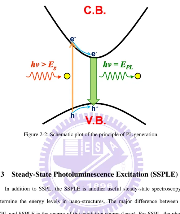
The steady-state luminescence spectrum is the fundamental spectroscopy for semiconductors which determines the energies of the emission photons generated from the recombination process. As shown in Fig. 2-2, photons with energy higher than the one of band gap (Eg) are input to pump the electrons from V.B. to C.B.; the holes and electrons relax to lower states and then recombine to generate PL. For the measurement of this kind, the detection focuses on different luminescence energies and is in steady-state condition. The excitation will generally be a photon source such as a laser because of the experimental convenience, giving the name to the analysis as
photoluminescence; however, the excitation source can vary to be others like a bias
Figure 2-2: Schematic plot of the principle of PL generation.
2.3 Steady-State Photoluminescence Excitation (SSPLE)
In addition to SSPL, the SSPLE is another useful steady-state spectroscopy to determine the energy levels in nano-structures. The major difference between the SSPL and SSPLE is the energy of the excitation source (laser). For SSPL, the photon energy of the laser is usually fixed while in SSPLE an energy-tunable photon source is used. It is well known that the input photons will only be absorbed by electrons in valence band to jump to conduction band when the energy of the input photons matches the energy difference between the two quantum states. Therefore, we can determine the energy levels by varying the energy of the input photon and monitor the PL intensity.
2.4Time-Resolved Photoluminescence (TRPL)
Unlike steady state measurement whose spectrum is resolved in frequency domain, time resolved photoluminescence deals with the spectroscopy in time domain, or the time dependence of photon generation. Imagine a specially-made ball whose color will change every millisecond. If one wishes to record all the colors that it reveals within a long time interval by a camera, the time interval between two shots of the camera must be less than one millisecond, or otherwise, some information will definitely be lost. Similarly, only by using a detection method with detection speed faster than it of the dynamic event itself can we ensure that the dynamic behaviors are completely recorded. In order to detect the event of carrier relaxation (picosecond order) and recombination (nanosecond order), the time resolution of the measurement techniques must be at least comparable (or faster) to them. Here we introduce the main principles of the three most commonly used methods for studying time-resolved spectroscopy in semiconductor nanostructures.
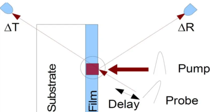
Pump-probe spectroscopy
The pump-probe spectroscopy is basically the application of optics. As shown in Fig. 2-3, a laser pulse is initially divided into two, the “pump” and “probe” beams, and a time delay Δt will be deliberately given between the two; the pump bean is targeted to excite the sample, while the other is used for probing the dynamic signal which will be collected by a detector. By adjusting Δt, one can get the time-dependent spectrum, which can be reflectivity, absorption or luminescence.
A commanding advantage of this approach will be the time resolution; ideally, its resolution is only determined by the pulse width of the laser [33], and by using the
laser with ultra-short pulse width, one can easily reach to an ultra-fast detection capability of femtosecond order or even higher.
Figure 2-3: Main principle of the pump-probe technique. (Source: Z. Sun,” Time Resolved Pump-Probe Spectroscopy.”)
Streak Camera
[34]A typical streak camera system is shown in Fig. 2-4. The signal generated by the sample will be focused to one photocathode to excite photoelectrons. The photoelectrons then are accelerated by an ultra high voltage to enter the sweep field, which provides a time-varying voltage. Finally the photoelectrons are reached on a screen for detection.
With this approach, one can directly get the data in a large detection range and it is very useful in some research aspects. Nonetheless, its time resolution can only be reached to the order of picosecond due to the limitation of the sweep rate of electronic devices.
Figure 2-4: Main principle of the steak camera technique. (Source: “Guide to Streak Cameras,” Hamamatsu Photonics.)
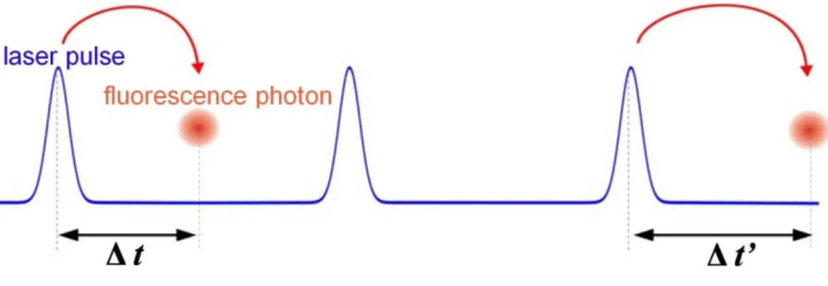
Time Correlated Single Photon Counting
[35]The major principle of Time Correlated Single Photon Counting (TCSPC) is a fairly smart one, mainly making use of the concept of statistics. Referring to Fig. 2-5, the measurement is proceeded by averagely allowing one or no photon between two laser pulses. When a photon appears, the time interval (Δt) will be recorded to complete a detection event, and the procedure will carry on repeatedly. Although Δt may be different from every event, one can get a statistically reliable result after a large quantity of repeated detections, as shown in Fig. 2-6.
Generally, the time resolution of TCSPC method can be reached to the order of picosecond, usually limited by the speed of the detectors. A great advantage about TCSPC method is the capability of detecting signal with low intensity by choosing suitable detectors such as photomultipliers (PMTs) or avalanche photodiodes (APDs); furthermore, the system is quite simple so that it is possible to additionally assemble it on the existing-experimental system by only adding several instruments.
Figure 2-5: Main principle of the TCSPC technique. (Source: Reference. 35.)
Figure 2-6: Final statistical integration of signal in the TCSPC technique. (Source: W. Becker, A. Bergmann,” Detectors for High-Speed Photon Counting.”)
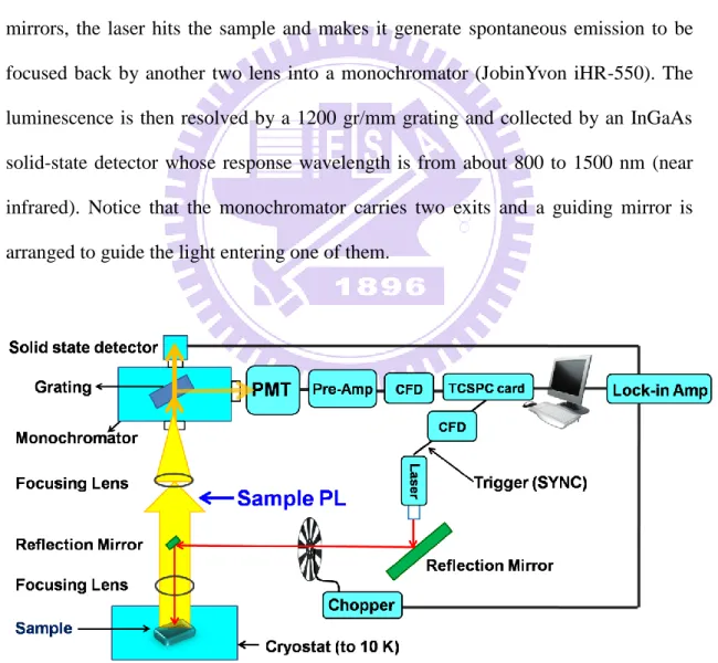
2.5 Experimental Setup in This Work
Steady-state PL
The steady-state luminescence spectra are obtained by PL in this work, and the apparatus is schematically drawn in Fig. 2-7. The sample is placed in a low-temperature (low-T) chamber with a closed-cycled helium cryostat used for temperature control; to increase the signal-to-noise ratio, a chopper and lock-in amplifier are applied. A diode laser (PicoQuant LDH-P-780, peak wavelength at 780 nm) is used as an external excitation source, and after passing through few reflection mirrors, the laser hits the sample and makes it generate spontaneous emission to be focused back by another two lens into a monochromator (JobinYvon iHR-550). The luminescence is then resolved by a 1200 gr/mm grating and collected by an InGaAs solid-state detector whose response wavelength is from about 800 to 1500 nm (near infrared). Notice that the monochromator carries two exits and a guiding mirror is arranged to guide the light entering one of them.
Time-resolved PL
The TRPL measurement is carried out by the TCSPC technique mentioned in the last chapter. The system is assembled additionally on the original set-up of the SSPL and the two actually share many common apparatus. The same diode laser is used for excitation except that the repetition rate is kept at 10 MHz in TRPL measurement while it is irrelevant in steady-state PL; moreover, both the laser beam and emitted luminescence undergo the same optical alignment as in the steady-state situation. As for the different aspects, first, the chopper and lock-in amplifier are not used and because of the dynamic measurement of TRPL, the detector must be able to “count” the signal as well, so an InGaAs photomultiplier tube (PMT, Hamamatsu H10330-75) is applied here. After selecting the detected wavelength, the guiding mirror in the monochromator is set to guide the light to the exit facing the PMT. Another difference resides in the final signal processing done by many delicate electronic devices, introduced as follows.
Beside the general laser beam used for excitation, an additional pulse signal is sent as a synchronization (SYNC) trigger and directly enters a constant fractional discriminator (CFD) to be a reference signal; the CFD acts as a threshold level to filter out the noise and judge whether the signal is valid. On the other hand, the luminescence signal will be detected by the PMT and then magnified by a pre-amplifier before entering the CFD. In the end, both signals enter the TCSPC counting card (Time Harp 200) for final statistical integration, as shown in Fig. 2-7, too.
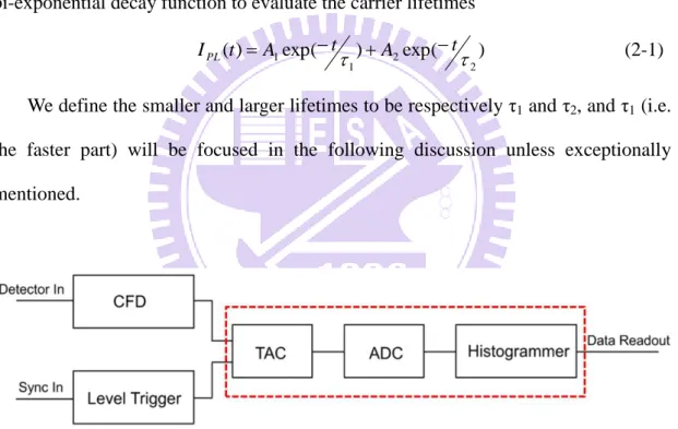
transforms the charge (voltage) signal to digital information of time to be inputted into the histogrammer. At this moment, one detection event is completed, and with numerous times of integration, one can get the time-dependent luminescence intensity like the one in Fig. 2-6.
Due to the system resolution is limited to be about 300 ps, it is only enough to detect the recombination dynamics but incapable for the relaxation. In other words, only the decay parts in the curves (Fig. 2-6) have the quantitative meaning whereas the rising will reveal merely the system resolution. For numerical fitting, we apply a bi-exponential decay function to evaluate the carrier lifetimes
) exp( ) exp( ) ( 2 2 1 1 t A t A t IPL (2-1)
We define the smaller and larger lifetimes to be respectively τ1 and τ2, and τ1 (i.e.
the faster part) will be focused in the following discussion unless exceptionally mentioned.
Figure 2-8: Final signal processing of the TRPL measurement. (Framed part: The electronic devices inside the TCSPC card.)
2.6 Fabrication of InAs QDs Samples
It cannot be overemphasized the essentiality of epitaxy in fabricating semiconductor nanostructures; if the crystal quality of the sample were already poor, the following study or further processed device would turn out to be in vain because of its natural imperfections. For instance, the interference of non-ideal effects due to poor crystal quality shall mask the original phenomena from our observation, not to mention its negative influence on device performance. Therefore, researchers have worked hard in these decades to improve the epitaxy techniques and have made a superior progress, including novel mechanical inventions such as molecular beam epitaxy (MBE) and metal organic chemical vapor deposition (MOCVD); nowadays, not only can we get samples with fine quality but many novel structures and materials can be put into new attempt.
The Stranski – Keastanov method
[14, 36, 37]To fabricate semiconductor QDs, the Stranski-Keastanov mode (S-K mode) epitaxy offers a reliable and convenient way. As shown in Fig. 2-9, a thin wetting layer is firstly deposited on a barrier layer (or simply a substrate); due to the lattice mismatch between the barrier and epitaxial material, strain quickly starts to pile up in the system; it is not until the critical moment that the structure can no longer sustain the accumulation of strain does the two-dimensional surface stop forming, changing into island or point-like shape to partially release energy of the system, and QDs are formed under this circumstance. A major key for this dimensional transition to occur is that the degree of lattice mismatch must be large enough for the two materials, for
The S-K mode approach has been widely applied in the growth of different nano-structures for both its uncomplicated procedures and capability for large number of output elements in one growth period.
Figure 2-9: Schematic plot of the Stranski-Keastanov mode formation.
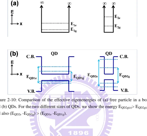
Quantized Energies of QDs
By varying the epitaxial conditions, we can control the size of the formed QDs, which is closely related to their intrinsic energy levels. Let us first recall a simple case. For a free particle inside a one-dimensional box of length L with infinite potential confinement, it is well-known that its ground state energy is inversely proportional to
L2, so is and the energy spacing between ground and first excited state. Qualitatively speaking, the energy and energy spacing will both be higher as long as the length of the box is shorter (Fig. 2-10(a)).
In fact, the case in QDs have a good analogy since it provides just a strong potential well for confining carriers, where the energy and energy spacing are higher (lower) for smaller (larger) QDs, as shown in Fig. 2-10 (b).However, except the size of QDs, there are still other factors which determine the energy levels such as the intermixing of matrix and QD materials; for just a gradual view and simplicity, we treat the energy level and energy spacing to be effectively higher (lower) as the size of
Figure 2-10: Comparison of the effective eigenenergies of (a) free particle in a box and (b) QDs. For the two different sizes of QDs, we show the energy EQD2g(e)> EQD2g(e),
and also (EQD2e -EQD2g) > (EQD1e -EQD1g).
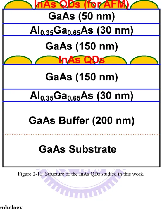
Sample structure
Six self-assembled InAs QDs samples grown by MBE on (100) GaAs substrate are studied in this work; their structures are basically the same shown in Fig. 2-11. A relatively thick GaAs buffer layer is firstly deposited on the substrate; the self-assembled QDs were embedded in GaAs matrix and sandwiched with Al(Ga)As confinement layers. Finally, uncapped QDs were grown on the surface with the same growth conditions of the embedded ones for morphology measurement. In addition, the QDs layer of the six samples were grown under different growth temperatures and
Figure 2-11: Structure of the InAs QDs studied in this work.
Morphology
The morphology measurement is done by using atomic force microscopy (AFM), one of the most powerful methods for obtaining surface information. The AFM of the six samples are shown in Fig. 2-12 (a) to 2-12 (f) with the scale of 1×1 μm2. For simple comparison, information including growth conditions, average QD density (D) width, height, and the corresponding sample numbers are all listed in Table 2-1.
Figure 2-12: AFM images of samples. (a) A (LM4682), (b) B (LM4681), (c) C (LM3572), (d) D (LM3573), (e) E (LM3472) and (f) F (LM4596).
Sample # Tgrowth (oC) MLs D (1010/cm2) Width (nm) Height (nm)
A (LM4682) 500 3.0 6.0 54.6 8.3 B (LM4681) 500 2.4 6.8 54.5 5.1 C (LM3572) 480 2.4 8.2 62.4 2.8 D (LM3573) 480 2.4 13 70.4 2.2 E (LM3472) 480 2.6 4.5 39 4.2 F (LM4596) 480 2.0 2.8 31.2 1.9
(b)
(a)
(d)
(c)
(f)
(e)
Chapter 3
Experimental Observation
In this chapter, we begin to introduce the results of our experimental work: the steady-state and time-resolved spectra of InAs/GaAs QDs. For time-resolved spectra, although there are totally six samples studied, the discussion will be firstly focused on two of them (sample A and C) for clear comparison. We present the first observation of an anomalous spike in the temperature-dependent TRPL around 45 – 85 K, and the spike is shown to be considerably suppressed by high excitation power. Furthermore, several InAs QDs samples with different sizes are studied, and we find that the spike will only occur in the QDs with a particular range of luminance energies.
3.1 Basic Determinations
Steady-state PL spectraFig. 3-1 shows the normalized SSPL spectra of the six samples measured at T = 25 K under the excitation of a 780-nm laser, with their full-width-at-half-maximum (FWHM) and ground state emission peaks ranging from 1.08 to 1.30 eV, listed in Table 3-1; the non-delta like emission energy is caused by the size-nonuniformity of the ensemble QDs, but in average, we can tell that the size is the largest for Sample A and the smallest for Sample F. In addition, although their FWHM are different among the six samples, we will show that it is irrelevant to the observation.
The steady-state PL is also a necessary work for the determination of detection points for the following TRPL measurement; each TRPL spectrum is detected under a particular PL energy, and unless specially mentioned, the detection points which we
0.9 1.0 1.1 1.2 1.3 1.4 1.5 1.6 0.0 0.2 0.4 0.6 0.8 1.0 1.2 F E C B A P L I n te n s it y ( a rb . u .)
Photon energy (eV)
D
Figure 3-1: SSPL spectra @ T = 25 K of the six samples.
Sample # A (LM4682) B (LM4681) C (LM3572) D (LM3573) E (LM3472) F (LM4596) Energy (eV) 1.08 1.15 1.20 1.25 1.27 1.30 FWHM (meV) 33 96 90 69 56 98 Table 3-1: List of peak energies and FWHM of the six samples studied in this work.
Steady-state PLE spectra (selective samples)
In addition to SSPL, the SSPLE measurements on four selective samples (sample A, C, D, and E) are done at T = 77 K (liquid nitrogen) using a Ti-sapphire laser shown in Fig. 3-2. The horizontal axis of the figure represents the energy difference between the energy of laser (Eexc) and a fixed detection PL (Edet); the detection PL points are chosen to be the ones corresponding to the (ground state) peak intensities of SSPL spectra at 77 K, and for a particular data point, it means the response of the state higher than ground state with spacing E – E . The result shows an analogy for all
respectively, which the other three samples also show the similar behaviors at higher energies. 0 50 100 150 200 250 300 350 400 450 500 1E-3 0.01 0.1 1 P L I n te n s it y ( a rb . u .) E
exc- Edet (meV)
A, Edet= 1.08 eV C, Edet = 1.20 eV D, Edet = 1.24 eV E, Edet = 1.26 eV
Figure 3-2: SSPLE spectra @ T = 77 K of the four selective samples.
Calculation of numbers of injected electron-hole pairs
The excitation power in the TRPL measurement actually correlates the numbers of injected electron-hole (e-h) pairs per QD per laser pulse, calculated by the following formula:
s
e
laser avg r x x s E R P N 1 exp exp , (3-1)where Navg is the average numbers of injected electron-hole (e-h) pairs per QD per laser pulse; P is the average input power; R is the repetition rate; Elaser is the photon energy of the laser; s means the area of the laser spot; r is the light reflection percentage at the sample surface; α is the absorption coefficient of GaAs at 780 nm. Referring to Fig. 2-11 for the structure of the sample, only the two 150nm-GaAs layers adjacent to the embedded QDs will contribute the injected e-h pairs into QDs;
starting and ending points of these GaAs layers; notice that the Al0.35Ga0.65As layers
do not respond to the excitation so their thicknesses are neglected. Moreover, by covering metal except several windows of different sizes (order of μm) left opened on the sample surface, the spot size of the laser can be estimated by adjusting the spot into different windows and checking the intensity of the PL signal. As a result, the spot size is estimated to be roughly 60 μm in diameter. For the other parameters, we list them in Table 3-2 with the calculated result under P = 25 μW for sample A (with QD density = 6.0×1010 cm-2) as an example.
P
(μW)R
(Hz)E
laser (eV)s
(μm2)r
(%)α
(cm-1)x
s (nm)x
e (nm)N
avg25 107 1.59 2827.4 30 1.4×10⁴ 50 150 1.13
Table 3-2: List of parameters used for the calculation of injected e-h pairs.
A Typical result of Temperature-Dependent TRPL of InAs QDs
Being able to fabricate InAs QDs on GaAs matrix in the 1990s [38, 39], the temperature-dependent (T-dependent) TRPL has been widely studied and come up with certain widely-accepted conclusions on both experimental observation and theoretical understanding.
Fig. 3-3 (a) shows the result of T-dependent TRPL of sample A under the excitation of 25 μW (average power), demonstrating a typical and well-known result. At low temperature (25-75 K), excitons are “frozen” to have no other special behaviors and the carrier lifetimes in this case are equal to the radiative lifetime, nearly unchanged to be about 0.85 ns. As temperature is raised higher enough to
thermal equilibrium gradually builds up among dot ensembles, known as the effect of “carrier redistribution” [23, 25-27]. As a result, the carrier lifetime increases accompanied by the decrease of FWHM of PL spectra, and the two are clearly observed in our case from 85 to 180 K in Fig. 3-3 (a) and (b). If the temperature is raised higher to near room temperature, the non-radiative recombination becomes dominating [22-24] and consequently cause the carrier lifetimes to decline with a severe drop in integrated PL intensity.
3.2 Low-Temperature Spike of Carrier Lifetimes
3.2.1 Observation and comparison
Compared to the well-known TRPL result for sample A, a surprising result is found in sample C, where an abnormal spike is clearly observed in the range of 50 to 75 K, plotted in Fig. 3-4 (a). In contrast to Sample A, the carrier lifetime of Sample C at 45-85 K behaves a totally distinct way, where it dramatically increases from 1.1 to 4.1 ns from 45 to 60 K, and then decreases back to 2.5 ns at 85 K, showing a spike-like shape; it is worth mentioning that this feature occurs in such a small range which reveals its critical sensitivity to environmental temperature.
At first glance the uncommon phenomenon, one may suspect that the sharp increase and decrease of carrier lifetimes are respectively the deserved consequences of carrier redistribution effect and non-radiative process. None the less, from the PL intensity and FWHM data plotted in Fig. 3-4 (b), we can tell that the physical origins of them are quite different. Firstly, the FWHMs of both samples come to a minimum in the middle temperature range, showing the redistribution effect of thermalized carriers and is responsible for the rise of lifetime in this regime. In addition, the PL intensity decays all the way up to room temperature for both samples due to the growing non-radiative recombination, accompanied with the falling carrier lifetimes. However, in the temperature range which the spike occurs, the trends of both PL intensity and FWHM for the two samples are nearly the same despite their entirely different behavior of carrier lifetimes. Accordingly, we can conclude that the abnormal spike is not resulted from the two well-known mechanisms.
0 50 100 150 200 250 300 0.5 1.0 1.5 2.0 2.5 3.0 3.5 4.0 4.5
C
a
rr
ie
r
L
if
e
ti
m
e
(
n
s
)
T (K)
Sample A - 25 W Sample C - 20 W(a)
Figure 3-4: (a) Observation of low-T spike phenomenon in sample C; a typical result is shown in Sample A for comparison. (b) Corresponding integrated PL intensity and FWHM for both two samples.
3.2.2 Energy-dependent TRPL
The energy-dependent TRPL of the two samples also studied and the results are plotted in Fig. 3-5 (a) and (b). Except for the peak value of ground state, the TRPL measurements are done under two additional energies, one is higher (represents smaller QDs) and the other is lower (represents larger QDs); we find that for both two samples at the middle temperature range, the carrier lifetimes of different QDs’ sizes show a distinction where lifetime of the smaller QDs becomes faster than the larger ones. This can be again attributed to the carrier redistribution effect but from another aspect: the thermalized carriers will escape from smaller QDs and then be recaptured by the larger ones with lower quantized energies; effectively speaking, more portions of total carriers enter the larger QDs, followed by the longer carrier lifetimes. Furthermore, the temperature which the effect begins to reveal is a little higher for Sample A, due to the need of more thermal energy for carriers at lower quantum states to escape from QDs.
In contrast, the carrier lifetimes in the spike regime of sample C are almost quantitatively the same for different detection energies, being another striking evidence for an individual type of its responsible mechanism.
3.2.3 Power-dependent TRPL
To further investigate the mechanism of the low-T spike, we have performed power-dependent TRPL measurement of sample C as shown in Fig. 3-6. It is clearly observed that the spike in 45 – 85 K becomes much more obvious under lower excitation and will be considerably suppressed by high power injection; at the lowest excitation power in our measurement (2 μW, corresponding to about 0.07 electron-hole pair per QD per pulse by the calculation of Eq. 3-1), the peak lifetime is as high as 7.6 ns. This feature illustrates that the related mechanism of the low-T spike concerns the carrier numbers in QDs.
30 40 50 60 70 80 90 100 110
0
1
2
3
4
5
6
7
8
C
a
rr
ie
r
L
if
e
ti
m
e
(
n
s
)
T (K)
Sample C 2 W 5 W 10 W 20 W 40 W3.2.4 Decay curves of PL intensity
The carrier lifetimes are the numerical results extracted by mathematical fitting. For a more fundamental perspective, let us now focus on the decay curves directly obtained from the time-resolved measurement under low power excitation, plotted in Fig. 3-7 (a) and (b) for sample A and C, respectively. Note that the PL intensity is in logarithmic scale so the slope of the curve is directly proportional to the inverse of carrier lifetime; the dash lines in the figures just indicate the two exponential components (see Eq. 2-1) of the curves, where the line with light (dark) color represents τ1 (τ2). For Sample A, the slopes of both faster and slower part of the decay
curves are almost unchanged from 35 to 100 Kelvin, correctly reflecting the fixed lifetimes in Fig. 3-4 (a). Yet, things are absolutely different when it comes to the other sample. For sample C, one can inspect that the faster part of the decay curve is being gradually substituted by the slower as temperature is raised from 35 to 50 K, and finally at T = 55 K, the slower part obtains absolute predominance and causes the faster part to totally disappear which makes the original τ2 now becomes the new τ1.
Mathematically speaking, the lifetime evaluated as T = 55 K is, however, no longer the faster τ1 but the slower τ2, resulting a radical increase in carrier lifetime. In other
words, the low-temperature spike occurs at the very temperature which the slower part in the decay curve completely replaces the faster, which is 55 K (Tspike = 55 K), and the it actually contains the information of both τ1 and τ2 regardless the lifetimes
reveal just the faster component in each time trace. Furthermore, as temperature rises higher than 55 K, the carrier lifetimes begin to gradually decrease till 75 K and finally re-increases at 85 K.
Figure 3-7: Measured decay curves under excitation power of 2 μW for (a) Sample A and (b) Sample C with their corresponding τ1in the inset figures.
respectively show the τ1 and τ2 for Sample A and C, and the ratio of A2/(A1+A2)
(named as “A2 ratio”) is shown in Fig. 3-8 (c); in this way, we can have a more
fundamental view on the behavior of the two part of the decay curves. For Sample C, we find that at T = 55 K, the two lifetimes are so close (τ2/τ1 < 2) that the curve can
somewhat be treated as a mono-exponential decay function; moreover, its A2 ratio
increases to a maximum of 0.42 at this temperature and then suddenly drop to an order below afterwards which shows that the curves for T = 60 – 100 K indeed behave as mono-exponential decay functions, too.
Comparatively for Sample A, its A2 component remains to be neglectable values
while τ2 still decreases with the rising temperature to 75 Kelvin. Moreover, its A2 ratio
somehow increases from 60 to 75 K (A2 ratio = 0.16), and τ2 decreases to the value
closet to τ1 as well at this temperature. Based on all the observations mentioned, it is
fair to argue that the phenomenon exists both in the two samples but somehow the
increment degree of A2 ratio is large enough to reveal it more clearly.
30 40 50 60 70 80 90 100 110 1 10 1 2 C a rr ie r L if e ti m e ( n s ) T (K) Sample A (a) 30 40 50 60 70 80 90 100 110 1 10 2 Sample C C a rr ie r L if e ti m e ( n s ) T (K) (b) 1 30 40 50 60 70 80 90 100 110 0.0 0.1 0.2 0.3 0.4 0.5 A 2 r a ti o T (K) Sample A Sample C (c)
3.3 The Prolonged Rising Time
As mentioned previously that the time resolution of our system is too low to measure the picosecond-order carrier relaxation; in other words, the rising time of the photon intensity will be approximately the value of our system resolution. Nevertheless, we show in Fig. 3-9 (a) and (b) that for Sample C, the rising time is qualitatively prolonged to the degree detectable for the system (~ 1 ns) as temperature rises whereas no such phenomenon is observed in Sample A.
Figure 3-9: Rising parts (measured in our system) of (a) Sample A and (b) Sample C.
3.4 Size Dependence of QDs on the Low-T Spike
The previous comparison of TRPL results are focused on the two samples and the spike somehow occurs only in the one with higher quantized energy. To check whether this phenomenon is dependent on the sizes of QDs, we bring the other four samples into study.
Fig. 3-10 shows the T-dependent carrier lifetimes of all the six samples under the excitation of 10 μW (due to experimental limitation, the lowest excitation power measured for Sample F is 10 μW; however, the power is low enough for qualitatively observation in all samples). We discover a surprising result that within this wide range
will reveal the spike-like feature. Moreover, although the spike are shown only in the three samples with intermediate ground state energies: Sample C (1.20 eV), Sample D (1.25 eV), and Sample E (1.27 eV), the peak values of carrier lifetimes among them remain an obvious difference, being the highest for Sample D.
30 40 50 60 70 80 90 100 110
1
10
C
a
rr
ie
r
L
if
e
ti
m
e
(
n
s
)
T (K)
Sample A Sample B Sample C Sample D Sample E Sample FFigure 3-10: T-dependent carrier lifetimes (τ1) for all six samples under 10 μW.
In addition, except the two previously discussed, the decay curves under the lowest excitation of the other four samples are shown in Fig. 3-11 (a) to (d) with their corresponding carrier lifetimes, and the fitting parameters for each of them are shown in Fig. 3-12 (a) to (e) to meet the completeness of the whole study.
A similar trend is observed that τ2 decreases as temperature rises. However, the
A2 component barely has the portion of less than 10 % in the decay curves for all
samples except Sample D; for Sample D, A2 violently increases to the value even
demonstrates that the phenomenon may be universal but it is the increment degree of A2 ratio which matters (sample C and D).
Figure 3-11: Measured decay curves of (a) Sample B, (b) Sample D, (c) Sample E and (d) Sample F with their corresponding τ1 in the inset figures.
30 40 50 60 70 80 90 100 110 1 10 1 C a rr ie r L if e ti m e ( n s ) T (K) (a) Sample B 2 30 40 50 60 70 80 90 100 110 1 10 1 2 C a rr ie r L if e ti m e ( n s ) T (K) (b) Sample D 30 40 50 60 70 80 90 100 110 1 10 1 2 C a rr ie r L if e ti m e ( n s ) T (K) (c) Sample E 30 40 50 60 70 80 90 100 110 1 10 1 2 C a rr ie r L if e ti m e ( n s ) T (K) (d) Sample F 30 40 50 60 70 80 90 100 110 0.0 0.2 0.4 0.6 0.8 1.0
A
2r
a
ti
o
T (K)
sample A - 2 W sample B - 2 W sample C - 2 W sample D - 10 W sample E - 2 W sample F - 10 W(e)
Figure 3-12: Fitting parameters of all six samples. (a) to (d): τ1, τ2 of sample B, D, E
3.5 Issues about the Sizes of QDs
Although the size dependence of the low-T spike is demonstrated in the last section, things are more complicated than we think. The steady-state PL spectra (Fig. 3-1) show that there exists an overlapping range for Sample C and B; according to the size-dependent argument mentioned in section 3.4, one may predict to observe the low-T spike if measuring TRPL under similar detection wavelength, regardless which sample we choose. Unexpectedly, this is not the case; referring to Fig. 3-13 (a) and (b), we find that in spite of the close detection energies (ε1, ε2 and ε3 equal to respectively
1.15, 1.20 and 1.16 eV) of the two samples, the spike is only observed in Sample C (ε3).
The “sample-dependent” observation indicates that the conditions for the spike to occur are not merely the size of QDs and excitation power but also other factors; the complexity of these factors may play a critical role, for instance, the distribution of strain for different QDs’ shapes or the dependence of intrinsic relaxation on energy spacing. However, these extra considerations are not discussed in this work.
Figure 3-13: (a) SSPL spectra for sample B and C. The detection energies of TRPL are ε1, ε2 for sample B and ε3 for sample C; (b) corresponding τ1 at different
Chapter 4
Simulation and Comprehension
To establish a comprehensive picture of the experimental observation, we propose a theoretical model involving three excitonic states in our simulation work. The model is solved numerically in rate equations and the output decay curves are then fitted by exactly Eq. 2-1 to evaluate τ1 and τ2 to be the faster and slower carrier lifetimes,
respectively. In addition to the simulation result, most importantly, the related physical significances are investigated, which analyzes the capability and limitation of this model to clarify the perspectives in future works.
4.1 Dark, Bright and Hot States (Excitons)
For InAs QDs, the confinement provided by the system is fine enough for both electrons and holes, so it is reliable to treat them together as excitons. The model used for simulation involves three quantized excitonic states in QDs: the dark, bright and hot states. They are shown in Fig. 4-1 and we now introduce the physical pictures for each of them.
The dark and bright states are actually closely related. Fig. 4-2 schematically shows the main difference between the two; the degeneracy of the ground state is spilt due to the exchange coupling between the spins of electron and hole for bright excitons, which let dark excitons attain the total angular momentum to be ± 2ℏ while for bright excitons the value is ± ℏ; the energy splitting between the two (Δgd) is typically few hundreds of μeV with the bright level above [40]. However, recombination is only allowed for bright excitons because of the restriction of selection rule, and for the other that cannot recombine, excitons are optically inactive, or “dark”. As for the hot state, it is formed by either the electron or hole at its ground state and the other at its first excited level.
Figure 4-2: Spin alignments of excitons; total spin angular momentum = (a) - ℏ, (b) ℏ, (c) 2ℏ and (d) - 2ℏ; (a) and (b) are bright excitons while (c) and (d) are dark excitons.
A Short Review on the Spin-Flip Relaxation
The spin dynamics in self-assembled QDs has caught great attention not only because the curiosity to further discover the fundamental behavior of QDs but with the expectation on the application of spintronic-based devices. In fact, the relevant
much less effective for sub-levels in QDs. On the other hand, it is argued that the hyperfine effect, or the interaction between electrons and nuclei is the dominant mechanism for the relaxation [42, 43]; the admixture of two independent spinors [41], spin-orbit coupling of holes in V.B. [44], phonon interaction and the mixing of light- and heavy-hole bands [45] are all proposed by theoretical researchers. However, the calculated spin-flip rates attributed to the above mechanisms fail to meet the experimental value, which is much faster [46, 47]. Thrilling, Liao et al. [48] recently studied the hole-Dresselhaus spin-orbit coupling and it leads to a result close to the observed values in InAs QDs [46]. As for our case, we now solve that rate equations based on the three-level system and study the spin dynamics theoretically together with the experimental data.
Carrier Transitions in the System
Since we are dealing with the dynamic behaviors of carriers, the state-to-state transition must be considered in detail. In spite of recombination is forbidden at dark state, it is allowed supposing that excitons can relax back to bright state by a spin-flip process mediated by phonons. However, it is reported that the spin-flip time, or τspin-flip, is fairly long to be about 100 ns at low temperature [46] compared to the usual radiative lifetime (1 ns) for InAs self-assembled QDs.
In contrast to the very slow transition process between the dark and bright state, the relaxation from hot state to either ground or bright states can be pretty fast. In fact, the issue was under debate in a period; some research groups report the existence of “phonon bottleneck” which results a long relaxation time (~ ns) [49, 50], whereas a great amount of recent works conversely deny the contention and advocate the
so contradictory, we believe the latter is more likely in our case since the energy spacing in this case is in the order of meV, reasonably making the carrier relaxation much more effective.
4.2 Rate Equations
Rate equations are useful for characterizing the carrier dynamics among various states in a system; with distinct transition rates, the dynamics can be so different. For example, the spin-flip relaxation from dark to bright state will be much slower than the relaxation from hot to bright state, even if the two events equally represent a transition from one level to another. The main goal of solving rate equations is to monitor the carrier variations with respect to time in particular states, which further helps us create correspondence in the existing experiments. For the three-level system referring to the states shown in Fig. 4-1, the mathematical expressions contain three differential equations with each of them coupled with the other two, which are:
. 1 1 1 1 , 1 1 ) ( 1 1 , 1 1 ) ( 1 1 h h dh d h h gh g d d hd h g g hg h h d d hd h d d gd g d h h dh d g g dg d d g g hg h g g dg d g h h gh g d d gd g rad g g n N N n N N n N N n N N dt dN n N N n N N t G n N N n N N dt dN n N N n N N t G n N N n N N N dt dN (4-1)
The subscripts “d”, “g”, and “h” respectively represent the dark, ground and hot states. Since we are only interested in the “decaying” behavior instead of the rising, we let the carrier generation be initially at ground and dark state with a Gaussian distribution, Gi(t); as regards the hot state, we assume that all carriers will be captured
As for the important transition, τrad is the radiative lifetime of excitons, and for the
transition time from a lower to the hot state, we consider the case of thermalized carriers whose distribution follows the Maxwell-Boltzmann statistics:
T k g hd h g d B g hd
e
) ( ) ( ) (
, (4-2)where kB is the Boltzmann constant, τhd(g) being the transition lifetime from the dark (d) or ground (g) to hot state (h) and vice versa with the energy spacing of the two equals to Δ. For the spin-flip rate, it has been discussed in many papers both experimentally [46] and theoretically [45, 48, 56]; however, due to the very small Δgd, here we assume the rate to be a constant (τgd = τdg = τspin-flip) independent of either Δgd or temperature for simplicity, and it will be clear that the exact value of τspin-flip is unimportant as long as it is large enough. Lastly, non-radiative recombination is not considered according to the SSPL intensity showing a nearly constant value below 100 Kelvin (Fig. 3-4 (b)). After setting the initial parameters, the rate equations are numerically solved using first-order approximation with dt = 0.1 ps (Eqs. 4-1). Finally, the decay curves of the bright state are obtained and the carrier lifetimes are then extracted by fitting the curves with Eq.2-1. As a whole, we give a flow chart in Fig. 4-3 to summarize the simulation procedures more clearly.
4.3 Simulation Results
By setting the values of parameters all with widely-accepted numbers listed in Table. 4-1, we can get the respective results of τ1 and τ2 plotted in Fig. 4-4 (a) and (b).
The result shows that the simulated τ1 is quantitatively well-fitted to the experimental
data from 35 and 75 Kelvin while slight differences are shown for τ2 at 45 and 50
Kelvin. Notice that the inconsistence at 85 K of τ1 is caused by the re-increase of the
experimental values. However, referring back to Fig. 3-4 (a) and Fig. 3-5 (b), the carrier redistribution effect starts approximately at this temperature, so we believe it is due to the mechanism not taken into account in our simulation.
In fact, the critical transition from τ1 to τ2 can also be obtained in the simulation,
as shown in Fig. 4-5 of the decay curves, where one can clearly observe the change from bi-exponential to mono-exponential decay right at T = 55 K. On the other hand, the stimulated A2 ratio increases to as large as 0.64 at 50 Kelvin (Fig. 4-6) and as T >
55 K, the decay curve changes into mono-exponential decay, meaning A2 = 0.
Parameter
τ
radτ
hdτ
hgτ
spin-flipΔ
hgΔ
gdValue 1 ns 10 ps 10 ps 35 ns 28.7 meV 300 μeV
Parameter
#
n
gn
dn
eG
giFWHM
Value 0.25 2 2 16 13 % 100 ps
Table 4-1: Parameters used in simulation. #: numbers of excitons per QD per laser pulse; FWHM: FWHM of the Gaussian generation (specification of the pulsed laser: 70 ps). Ggi: portion of carriers initially given at the ground state.
30 40 50 60 70 80 90 100 110
0
1
2
3
4
5
6
7
8
(a)
Measued (Sample C)Simulated
1
(
n
s
)
T(K)
35
40
45
50
10
15
20
25
30
35
40
(b)
2
(
n
s
)
T(K)
Measured (Sample C) SimulatedFigure 4-4: Comparison of (a) τ1 and (b) τ2 with simulation and experiment. No
simulated data points of τ2 for T ≧ 55 K because the decay curves become
Figure 4-5: Decay curves obtained from simulation. The “transition” of the lifetimes as in the experimental case is clearly shown. Inset: corresponding τ1 of simulation.
Figure 4-6: A2 ratio at different temperatures with the corresponding τ1. For T ≧ 55 K,
4.4 Mechanisms – the Effect of Temperature
4.4.1 Main discussion
When it comes to modeling, the fit between the experiment data and theoretical prediction is basically the mathematical acquirement; what really matters is the valuable physical concept obtained from the simulation. It should be emphasized that temperature is the most substantial manipulated variable in this whole study so the following discussion will be centered on its effect.
Considering excitons occupying both dark and bright states at low temperature, for the lack of thermal energy, the only option for depleting dark excitons is to have them relax back to the bright states for recombination through a spin-flip process, whose rate is fairly slow (Fig. 4-7 (a)). In this case, the time-dependent PL intensity (PL time trace) of the bright state will indeed be a bi-exponential decay function where the faster part is due to the recombination of bright excitons while the slower is attributed to the recombination after the spin-flip process for dark excitons.
None the less, things become quite different as temperature rises. As shown in Fig. 4-7 (b), since carriers have enough thermal energy, they can be firstly thermalized to the hot state and then relax back to bright state for recombination; compared to the spin-flip relaxation, this additional path is such a much faster process that carriers prefer, and we believe that the spin angular momentum can be realigned with a larger probability during the process. Consequently, as temperature is raised, carriers are capable to continuously compensate the consumption of the radiative recombination from the additional path, making the decay rate to slow down and the measured τ1
prolonged significantly.