An electrically tunable-focusing liquid crystal
lens with a low voltage and simple electrodes
Hung-Chun Lin and Yi-Hsin Lin*
Department of Photonics, National Chiao Tung University, 1001 Ta Hsueh Rd., Hsinchu 30010, Taiwan *[email protected]
http://www.cc.nctu.edu.tw/~yilin
Abstract: An electrically tunable focusing LC lens with a low voltage and
simple planar electrodes is demonstrated. The inhomogeneous electric field of the LC lens without any hole-patterned-electrode is generated by using an embedded polymeric layer with a gradient distribution of dielectric constants (or relative permittivity). LC directors in the LC layer experience spatially inhomogeneous voltages even though a single voltage is applied to the planar electrodes. Such a LC lens has a low voltage (~2.6 Vrms) and
simple design of electrodes. The gradient distribution of dielectric constants of polymeric layer is discussed and the performance of the LC lens is investigated. The applications of such a LC lens are cell phones, webcam, and pico projectors.
©2012 Optical Society of America
OCIS codes: (230.3720) Liquid-crystal devices; (230.2090) Electro-optical devices. References and links
1. D. K. Yang and S. T. Wu, Fundamentals of Liquid Crystal Devices (John Wiley & Sons Ltd. Chichester, 2006), Chap. 12.
2. H. C. Lin, M. S. Chen, and Y. H. Lin, “A review of electrically tunable focusing liquid crystal lenses,” Trans. Electr. Electron. Mater. 12, 234–240 (2011).
3. H. C. Lin and Y. H. Lin, “A fast response and large electrically tunable-focusing imaging system based on switching of two modes of a liquid crystal lens,” Appl. Phys. Lett. 97(6), 063505 (2010).
4. H. C. Lin and Y. H. Lin, “An electrically tunable focusing pico-projector adopting a liquid crystal lens,” Jpn. J. Appl. Phys. 49(10), 102502 (2010).
5. Y. H. Lin, M. S. Chen, and H. C. Lin, “An electrically tunable optical zoom system using two composite liquid crystal lenses with a large zoom ratio,” Opt. Express 19(5), 4714–4721 (2011).
6. M. Hain, R. Glockner, S. Bhattacharya, D. Dias, S. Stankovic, and T. Tschudi, “Fast switching liquid crystal lenses for a dual focus digital versatile disc pickup,” Opt. Commun. 188(5-6), 291–299 (2001).
7. H. W. Ren, Y. H. Fan, and S. T. Wu, “Tunable Fresnel lens using nanoscale polymer-dispersed liquid crystals,” Appl. Phys. Lett. 83(8), 1515–1517 (2003).
8. G. Q. Li, D. L. Mathine, P. Valley, P. Ayräs, J. N. Haddock, M. S. Giridhar, G. Williby, J. Schwiegerling, G. R. Meredith, B. Kippelen, S. Honkanen, and N. Peyghambarian, “Switchable electro-optic diffractive lens with high efficiency for ophthalmic applications,” Proc. Natl. Acad. Sci. U.S.A. 103(16), 6100–6104 (2006).
9. G. Q. Li, P. Valley, M. S. Giridhar, D. L. Mathine, G. Meredith, J. N. Haddock, B. Kippelen, and N.
Peyghambarian, “Large-aperture switchable thin diffractive lens with interleaved electrode patterns,” Appl. Phys. Lett. 89(14), 141120 (2006).
10. G. Q. Li, P. Valley, P. Ayras, D. L. Mathine, S. Honkanen, and N. Peyghambarian, “High-efficiency switchable flat diffractive ophthalmic lens with three-layer electrode pattern and two-layer via structures,” Appl. Phys. Lett. 90(11), 111105 (2007).
11. P. Valley, D. L. Mathine, M. R. Dodge, J. Schwiegerling, G. Peyman, and N. Peyghambarian, “Tunable-focus flat liquid-crystal diffractive lens,” Opt. Lett. 35(3), 336–338 (2010).
12. A. F. Naumov, M. Y. Loktev, I. R. Guralnik, and G. Vdovin, “Liquid-crystal adaptive lenses with modal control,” Opt. Lett. 23(13), 992–994 (1998).
13. A. Naumov, G. D. Love, M. Y. Loktev, and F. L. Vladimirov, “Control optimization of spherical modal liquid crystal lenses,” Opt. Express 4(9), 344–352 (1999).
14. S. Kotova, M. Kvashnin, M. Rakhmatulin, O. Zayakin, I. Guralnik, N. Klimov, P. Clark, G. Love, A. Naumov, C. Saunter, M. Loktev, G. Vdovin, and L. Toporkova, “Modal liquid crystal wavefront corrector,” Opt. Express 10(22), 1258–1272 (2002).
15. N. Fraval and J. L. D. de la Tocnaye, “Low aberrations symmetrical adaptive modal liquid crystal lens with short focal lengths,” Appl. Opt. 49(15), 2778–2783 (2010).
17. M. Ye and S. Sato, “Optical properties of liquid crystal lens of any size,” Jpn. J. Appl. Phys. 41(5B), L571–L573 (2002).
18. B. Wang, M. Ye, and S. Sato, “Liquid crystal lens with stacked structure of liquid-crystal layers,” Opt. Commun. 250(4-6), 266–273 (2005).
19. B. Wang, M. Ye, and S. Sato, “Liquid crystal lens with focal length variable from negative to positive values,” IEEE Photon. Technol. Lett. 18(1), 79–81 (2006).
20. M. Ye, B. Wang, and S. Sato, “Realization of liquid crystal lens of large aperture and low driving voltages using thin layer of weakly conductive material,” Opt. Express 16(6), 4302–4308 (2008).
21. C. W. Chiu, Y. C. Lin, P. C. P. Chao, and A. Y. G. Fuh, “Achieving high focusing power for a large-aperture liquid crystal lens with novel hole-and-ring electrodes,” Opt. Express 16(23), 19277–19284 (2008).
22. M. Ye, B. Wang, M. Uchida, S. Yanase, S. Takahashi, M. Yamaguchi, and S. Sato, “Low-voltage-driving liquid crystal lens,” Jpn. J. Appl. Phys. 49(10), 100204 (2010).
23. K. Asatryan, V. Presnyakov, A. Tork, A. Zohrabyan, A. Bagramyan, and T. Galstian, “Optical lens with electrically variable focus using an optically hidden dielectric structure,” Opt. Express 18(13), 13981–13992 (2010).
24. H. C. Lin and Y. H. Lin, “An electrically tunable focusing liquid crystal lens with a built-in planar polymeric lens,” Appl. Phys. Lett. 98(8), 083503 (2011).
25. C. J. Chen, K. R. Sarma, and A. Kolosovskaya, “Capacitance–voltage characteristics of liquid crystal displays with periodic interdigital electrodes,” Appl. Phys. Lett. 74(1), 147–149 (1999).
26. I. C. Khoo and S. T. Wu, Optical and Nonlinear Optics of Liquid Crystals (World Scientific Ltd. London, 1993), Chap. 2.
27. H. Ren, Y. H. Lin, Y. H. Fan, and S. T. Wu, “Polarization-independent phase modulation using a polymer-dispersed liquid crystal,” Appl. Phys. Lett. 86(14), 141110 (2005).
28. Y. H. Lin, H. Ren, Y. H. Fan, Y. H. Wu, and S. T. Wu, “Polarization-independent and fast-response phase modulation using a normal-mode polymer-stabilized cholesteric texture,” J. Appl. Phys. 98(4), 043112 (2005). 29. H. Ren, Y. H. Lin, C. H. Wen, and S. T. Wu, “Polarization-independent phase modulation of a homeotropic
liquid crystal gel,” Appl. Phys. Lett. 87(19), 191106 (2005).
30. Y. H. Lin, H. Ren, Y. H. Wu, Y. Zhao, J. Fang, Z. Ge, and S. T. Wu, “Polarization-independent liquid crystal phase modulator using a thin polymer-separated double-layered structure,” Opt. Express 13(22), 8746–8752 (2005).
31. Y. H. Lin, H. S. Chen, H. C. Lin, Y. S. Tsou, H. K. Hsu, and W. Y. Li, “Polarizer-free and fast response microlens arrays using polymer-stabilized blue phase liquid crystals,” Appl. Phys. Lett. 96(11), 113505 (2010). 32. H. Ren, Y. H. Lin, and S. T. Wu, “Polarization-independent and fast-response phase modulators using
double-layered liquid crystal gels,” Appl. Phys. Lett. 88(6), 061123 (2006).
1. Introduction
Electrically tunable-focusing liquid crystal (LC) lenses have many applications, such as 3D displays, optical tweezers, imaging systems, and eye glasses. The electrically tunable focal length of LC lenses results from the electrically tunable distribution of refractive indices due to the orientations of LC directors controlled by applied electric fields. In addition, LC lenses are light and compact with low power consumption. Thus, LC lenses are very suitable for the applications of portable devices. However, high driving voltage (~90 Vrms), low lens power
(~5 Diopter) and small aperture (< 2 mm) of LC lenses still need to be solved for applications [1–5]. Several LC lenses are proposed for achieving low driving voltage, such as pixelated LC lenses (~5 Vrms) [6–11], LC lenses with modal controls (~10 Vrms) [12–15], LC lenses with a
hole-pattern-electrode and a weakly conductive layer (~3.5 Vrms) [16–22], and LC lenses with
two hidden dielectric layers (~20 Vrms) [23]. The driving scheme and the electrode design of
pixilated LC lenses are complicated. LC lenses with modal controls and LC lenses within a hole-pattern-electrode and an extra weakly conductive layer require a hole-pattern-electrode to generate inhomogeneous electric fields to the LC layer and the conductive layer requires a high driving frequency (~6000 Hz). LC lenses with two hidden dielectric layers do not need a hole–pattern-electrode; however, they have Fresnel reflections between two hidden dielectric layers and Fresnel reflections affect the image quality of LC lenses. The extra alignment layer is also needed to align LC directors. Recently, we proposed a LC lens with built-in polymeric layer to shift the range of tunable focus length [24]. However, the voltage is still high (~35-90 Vrms) and it requires a hole-patterned-electrode to generate inhomogeneous electric field to the
LC layer. In this paper, we demonstrate a LC lens without any hole-patterned-electrode and the inhomogeneous electric field to LC layer is generated by using an embedded polymeric layer with a gradient distribution of dielectric constants (or relative permittivity). LC directors in the LC layer then experience spatially inhomogeneous voltages even though a single voltage is applied to the planar electrode. Such a LC lens has a low voltage (~2.6 Vrms) and
simple design of electrodes. The gradient distribution of dielectric constants of polymeric layer is discussed and the performance of the LC lens is investigated. The applications of such a LC lens are cell phones, webcam, and pico projectors.
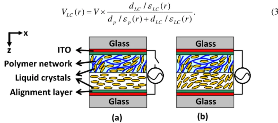
2. Structure and operating principles
The structure of the LC lens is depicted in Fig. 1(a). The LC lens consists of two ITO glass substrates coated with mechanically buffered PVA (Polyvinylalcohol) to align LC molecules, a LC layer and a polymeric layer. The polymer layer is composed of the polymer networks and liquid crystals. In the polymeric layer, the LC directors anchored among the polymer networks have a symmetric lens-like distribution of refractive indices and also a symmetric distribution of the relative permittivity (or dielectric constants). As a result, the polymeric layer has a fixed focal length with a non-uniform distribution of dielectric constants. The LC directors in the LC layer are then aligned homogeneously by the polymeric layer and the bottom alignment layer with pretilt angle ~2 degree. At the voltage-off state (V=0), the focal length of the LC lens (f(V)) comes from the polymeric layer only because of no phase difference in LC layer, as shown in Fig. 1(a). When the applied voltage exceeds threshold voltage (Vth), the LC layer experiences an inhomogeneous electric field due to the
non-uniform dielectric constants of the polymeric layer. The liquid crystal directors in the LC layer are then reoriented by the non-uniform electric field; therefore, the LC layer acts as a lens. The focusing properties of the LC lens depend on the focusing properties of two sub-lenses: one is the LC layer and the other is the polymeric layer. The total focal length (f(V)) of the LC lens can then be expressed as [24]:
1 1 1
,
( ) LC( ) p
f V f V f
= + (1)
where fp is the fixed focal length of the polymeric layer. The electrically tunable focal length
of the LC layer 2
( ) / 4
LC
f V =π×D ×λ× ∆δ , where D is the aperture width, λ is the
wavelength of the incident light and ∆δ is the phase difference between the center part and the border part of the aperture. The LC lens at a fixed location (x, y) along z-direction in Fig. 1(a) is equivalent to two capacitors connected in series resulting from the polymeric layer and the LC layer. The equivalent capacitor of the polymeric layer is defined as Cp(r), where r is (x2 +
y2)0.5. The equivalent capacitor of the LC layer is CLC (r). When we apply a voltage (V) to the
LC lens, the voltage on the LC layer (VLC(r)) can be expressed as:
1 / ( ) ( ) . 1 / ( ) 1 / ( ) LC LC p LC C r V r V C r C r = × + (2)
The capacitors Cp(r) and CLC (r) also depend on the thickness of the LC layer (dLC), the
thickness of the polymeric layer (dp), the dielectric constant of the LC layer (εLC(r)), and the
dielectric constant of the polymeric layer (εp(r)). The Eq. (2) can be further written as:
/ ( ) ( ) . / ( ) / ( ) LC LC LC p p LC LC d r V r V d r d r ε ε ε = × + (3) ITO Alignment layer Liquid crystals (a) x z Polymer network (b) z Glass Glass Glass Glass ITO Alignment layer Liquid crystals (a) x z Polymer network (b) z Glass Glass Glass Glass
When we apply the voltage to the LC lens, as Fig. 1(b) shows, we assume that the LC directors have not reoriented immediately and then the εLC(r)~εLC is a constant. The voltage
difference (∆VLC) in the center of the LC lens (i.e. r = 0) and the edge of the LC lens (i.e. r is
the radius of the LC lens) is VLC( )r −VLC(0)which can be expressed as:
/ / . / ( ) / / (0) / LC LC LC LC LC p p LC LC p p LC LC d d V V V d r d d d ε ε ε ε ε ε ∆ = × − × + + (4)
We defined ∆εp as εp(r)-εp(0) and dp equals to dLC in our structure. Equation (4) can be
simplified as: . [ ( )] [ (0)] LC p LC LC p LC p V V r ε ε ε ε ε ε × × ∆ ∆ = + × + (5)
In Eq. (5), in order to generate a voltage distribution to the LC layer when we apply a voltage (V) to the LC lens, we adopt a polymeric layer with a distribution of dielectric constant (i.e. ∆εp≠0). In Eq. (3), Eq. (4), and Eq. (5), we assume εLC(r) is a constant; however,
the variation of εLC(r) should be considered. The variation of εLC(r) under applied voltages
lowers VLC and also lowers ∆VLC. ∆VLC can be further re-modified after considering the
variation of εLC(r). εp(r) can be adjusted by the orientation of monomers which follows the
equation [25]: 2 2 / / ( ) sin ( ) cos ( ), p r r r ε ε θ ε θ ⊥ = + (6)
where ε// and ε⊥ are the dielectric constants of the polymeric layer which the electric fields
parallel and perpendicular to the long axes of monomer molecules. θ(r) is the tilt angle between the long axes of monomer molecules and the x-axis in Fig. 1(a). By adjusting the distribution of the dielectric constants of the polymeric layer, we can generate a spatial distribution of the voltages in LC layer even though we just apply a single voltage to the electrodes. The gradient refractive index distribution of the LC layer resulted from the spatial distribution of the voltage generates the lens-like phase difference ∆δ and thus the focal length of the LC layer. The driving voltage can also be reduced by controlling the distribution of the dielectric constants of the polymeric layer. Moreover, the smaller driving voltage V can be achieved by reducing the thickness of the polymeric layer dp form Eq. (3). Compare to the
glass substrate or the hidden dielectric layer which consists of two dielectric materials [23], the polymeric layer with thin thickness can be easily achieved. Therefore, the electrically tunable focus LC lens with low driving voltage and simple electrodes can be realized.
3. Experimental results and discussion
To fabricate the polymeric layer with gradient dielectric constant distribution, we first sandwiched NOA81 (Norland) between two ITO glass substrates and one of the glass substrate was etched with a hole-pattern within a diameter of 2 mm. Then we exposed UV light to solidify the NOA81, as shown in Fig. 2(a). The layer of NOA81 is an insulating layer between two electrodes. We coated the bottom substrate (in Fig. 2(a)) with the mechanically buffered polyvinyl alcohol (PVA) as the alignment layer and then prepared another ITO glass substrate coated with the mechanically buffered PVA. We then filled nematic LC (Merck, MLC 2070), reactive mesogen (Merck, RM 257), and photoinitiator (Merck, IRG-184) at 79:20:1 wt% ratios between two PVA layers, as shown in Fig. 2(b). The cell was then applied two voltages: V1 = 160 Vrms (f = 1kHz) and V2 = 27 Vrms (f = 1kHz). The reason why we used
two voltages is that we can obtain the continuous distribution of the electric field and also reduce the disclination lines of the polymeric layer. The call was then shined the UV light (~1.25 mW/cm2) for 1 hour at 70°C, as depicted in Fig. 2(b). After photopolymerization, we peeled off the glass substrates by a thermal releasing process and obtained the polymeric layer
on a PVA/ITO coated substrate, as shown in Fig. 2(c). Then we sandwiched nematic LC mixture MLC-2070 (Merck, ∆n = 0.26 for λ = 589.3 nm at 20°C) between the polymeric layer and another ITO substrate coated with mechanically buffered PVA as shown in Fig. 1(a). Both of the thicknesses of polymeric layer and LC layer (in Fig. 1 or Fig. 2(d)) are 25 µm. The fabrication process of the LC lens is similar to the previous work [5, 24], but we peel off the patterned top substrate in this design instead of non-patterned bottom substrate.
PVA NOA81 ITO Glass substrate UV LC+monomer LC Polymeric layer (a) (b) (c) (d) UV V1 V2 PVA NOA81 ITO Glass substrate UV LC+monomer LC Polymeric layer (a) (b) (c) (d) UV V1 V2
Fig. 2. Fabrication process of the LC lens. (a) NOA81 under UV exposure. (b) Mixture filling and then UV exposure. (c) Peel off the substrates. (d) Cell assembling.
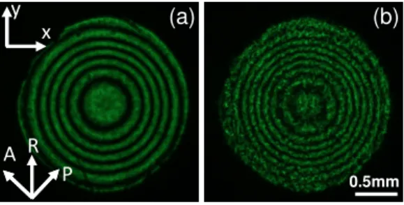
For observing the phase profile of the LC lens, we put the LC lens under crossed polarizers. The rubbing direction of the LC lens was 45° with respect to the transmission axis of one of polarizers. The observed images at 0 Vrms and 2.6 Vrms (f = 1kHz) ere shown in Fig.
3(a) and Fig. 3(b). In Fig. 3(a), the concentric rings of the LC lens at V = 0 indicate the phase profile of the polymeric layer. In Fig. 3(b), the concentric rings at 2.6 Vrms indicate the phase
profile of the combination of the polymeric layer and the LC layer. In Fig. 3(b), the concentric rings are not smooth because of scattering. By improving the thermal releasing process, the surface of the polymeric layer can be smoother and then improve the phase profiles. We also examined the polymeric layer only under applied voltages, and we found that the phase profile unchanged under different voltage (< 20 Vrms). That means the focal length of the
polymeric layer is fixed.
(b) (a) x y 0.5mm P A R (b) (a) x y 0.5mm P A R
Fig. 3. The phase profiles of the LC lens at (a) 0 Vrms and (b) 2.6 Vrms (f = 1kHz). λ = 532 nm.
P: the transmission axis of the polarizer, A: the transmission axis of the analyzer, R: the direction of alignment of the substrate.
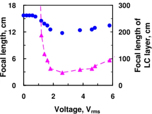
The numbers of concentric rings can be converted in to the focal length (f) by using the equation: f = D2/8λN, where D is the aperture size, λ is the wavelength, N is the number of concentric rings of the phase profile. The initial focal length of the LC lens is 15.6 cm determined by the polymeric layer. When the applied voltage is larger than the threshold voltage (~1 Vrms), the number of the rings increases because the focal length decreases. In Fig.
3(b), the focal length of the LC lens is 11.7 cm at 2.6 Vrms. The increased phase different is
around 4π caused by the phase different of the LC layer. Based on the phase profiles, we plotted the voltage-dependent focal length of the LC lens, as shown in Fig. 4. The focal length decreases from 15.6 cm to 11.7 cm as the applied voltage increases from 0 Vrms to 2.6 Vrms,
and then increase when the applied voltage is larger than 2.6 Vrms. In Fig. 4, the focal length at
0 Vrms is the focal length of the polymeric layer only. That means the LC lens can be operated
in a low driving voltage (< 2.6 Vrms) and simple electrodes without patterned-hole electrodes.
voltage according to Eq. (1). The focal length of the LC layer decreases from infinity to 47 cm as the voltage increases from 0 Vrms to 2.6 Vrms (pink triangles in Fig. 4). The focal length of
the LC layer then increases when the voltage exceeds 2.6 Vrms. When the applied voltage is
switched from 0 to 2.6 Vrms and from 2.6 Vrms to 0, the switching time is 2.5 seconds and 630
milliseconds, respectively. The slow rise time can be improved by the overdriving method [26]. In fact, the LC lens shows slightly scattering with an applied voltage because of three reasons. One is the mismatch of refractive indices between polymer networks and LC directors in the polymeric layer. The second is the imperfect alignment of LC directors in the LC layer due to the weak alignment capability of the polymeric layer. The third is the roughness of the polymeric layer which is controllable by adjusting fabrication process. Therefore, the scattering results from the roughness of the polymeric can be reduced.
0 6 12 18 0 2 4 6 Voltage, Vrms F o c a l le n g th , c m 0 100 200 300 F o c a l le n g th o f L C l a y e r, c m
Fig. 4. The focal length of the LC lens as a function of the applied voltage (blue dots) and the focal length of the LC layer as a function of the applied voltage (pink triangles). (f = 1kHz).
To calculate the distribution of the relative permittivity of the polymeric layer (∆εp (r) =
εp(r)-εp(0)), we calculated ∆n(r) which is defined as the difference of refractive indices
between the center (i.e. r = 0) and the edge of the LC lens (i.e. ∆n(r) = n(r)-n(0)). The measured refractive indices of the center of the polymeric layer is 1.78 (i.e. n(r = 0) = 1.78) which means the LC directors are aligned along x-direction in the center of the aperture in Fig. 1(a). n(r = 0) is obtained by measuring phase shift using Mach-Zehnder interferometer. The percentage of LC is high (~80 wt%) and therefore n(r = 0) is very closed to extraordinary refractive index of host LC (~1.78). ∆n(r) then can be obtained from Fig. 3(a) by applying the equation of phase retardation: Γ( )r =2π× ∆n r( )×d/λ , where λ is 532 nm and d is the
thickness of the polymeric layer. n(r) is then calculated. As a result, the averaged tilt angle (θ(r)) at different r can also be estimated according the Eq. (7)
2 2 2 2 2 1 cos ( ) sin ( ) , ( ) pe po r r n r n n θ θ = + (7)
where npe is 1.78 which is the refractive index of LC directors of the polymeric layer aligned
along x-direction for the x-linearly polarized light in Fig. 1(a), and npo is 1.52 which is the
refractive index of LC directors of the polymeric layer aligned along z-direction for the x-linearly polarized light in Fig. 1(a). We also measured ε// and measured ε⊥ of the polymeric
layer in Eq. (6) using a LCR meter (Hewlett Packard 4284A). As a result, εp(r) is obtained by
substituting the result of θ(r), the measured ε//, and measured ε⊥ (ε// = 14 and ε⊥ = 4.6) into Eq.
(6). The relative permittivity (εp (r)) as function of position (r) can be plotted in Fig. 5. The
relative permittivity increases from 4.60 to 8.66 from the center to the edge of the aperture of the LC lens. The phase distribution of the LC layer at different applied voltage is also illustrated in Fig. 6 according to the phase profile of the LC lens and the phase profile of the polymeric layer. In Fig. 6, the phase distribution of the LC layer is more parabolic with an
increase of an applied voltage. The larger phase difference of the LC layer between the center of the aperture (i.e. position is zero in Fig. 6) and the edge of the aperture (i.e. position is 1 mm or −1 mm in Fig. 6) represents the shorter focal length of the LC layer which agrees with the results in Fig. 4. From Fig. 5 and Fig. 6, the gradient distribution of relative permittivity of polymeric layer causes an inhomogeneous distribution of applied voltages even though we only apply a single voltage to the ITO electrode.
0
2
4
6
8
10
-1.0 -0.5 0.0 0.5 1.0Position, mm
R
e
la
tiv
e
p
e
rm
it
ti
v
it
y
Fig. 5. The distribution of the relative permittivity of the polymeric layer.
0 4 8 12 16 20 -1 -0.5 0 0.5 1 Position, mm Ph a s e , ra d ia n s 0 Vrms 1.4 Vrms 2.6 Vrms
Fig. 6. Phase distribution of the LC layer at 0 Vrms (red dotted line), 1.4 Vrms (blue triangles),
2.6 Vrms (black squares). (f = 1kHz).
Figures 7(a) and 7(b) show the image performances of the LC lens. The imaging system consists of a polarizer, the LC lens, a lens module with the effective focal length of 3.7 mm and an image sensor with 2 Mega pixels. The photos were taken under an ambient white light. The objects were at 7 cm away from the LC lens. The images are out of focused and focused when the applied voltage is switched between 0 Vrms and 2.6 Vrms, as shown in Fig. 7(a) and
7(b). The tunable focusing range of the LC lens is around ~2.14 diopter for the focal length is from 11.7 cm to 15.6 cm. To increase the tunable focusing range, we can increase ∆VLC to
enhance the distribution of the refractive indices of the LC layer. To increase ∆VLC, we can
enlarge ∆εp by using LC and monomers with high dielectric anisotropy or applying a large
gradient electric field during curing process.
(b)
(a) (b)
(a)
4. Conclusion
We have demonstrated an electrically tunable focusing LC lens with low driving voltages and a simple electrode without any hole-patterned electrodes. The operating voltage is low ~2.6 Vrms. The structure of the LC lens is simple and compact. We also demonstrated the image
performance by using the LC lens. We still need to improve the polarization dependency, slow response time and image quality. To remove the polarization dependency, we can change different LC mode in the LC layer [27–32]. The response time can be improved by improve the materials of LC, change the driving scheme or adopting the method of two mode switching [3, 26]. The LC lens with low driving voltages and a simple electrode can have great impacts in auto-focusing cell phones, webcam and cameras.
Acknowledgments
This research was supported by the National Science Council (NSC) in Taiwan under the contract no. 98-2112-M-009-017-MY3.