N A N O E X P R E S S
Open Access
A junctionless SONOS nonvolatile memory device
constructed with
in situ-doped polycrystalline
silicon nanowires
Chun-Jung Su
1,2, Tuan-Kai Su
2, Tzu-I Tsai
3, Horng-Chih Lin
2,4*and Tiao-Yuan Huang
2Abstract
In this paper, a silicon-oxide-nitride-silicon nonvolatile memory constructed on an n+-poly-Si nanowire [NW] structure featuring a junctionless [JL] configuration is presented. The JL structure is fulfilled by employing only one in situ heavily phosphorous-doped poly-Si layer to simultaneously serve as source/drain regions and NW channels, thus greatly simplifying the manufacturing process and alleviating the requirement of precise control of the doping profile. Owing to the higher carrier concentration in the channel, the developed JL NW device exhibits significantly enhanced programming speed and larger memory window than its counterpart with conventional undoped-NW-channel. Moreover, it also displays acceptable erase and data retention properties. Hence, the desirable memory characteristics along with the much simplified fabrication process make the JL NW memory structure a promising candidate for future system-on-panel and three-dimensional ultrahigh density memory applications.
Keywords: JL; NW, poly-Si, SONOS, TFT
Introduction
With the proliferation of portable electronic products, the demand of high density nonvolatile memories [NVMs] has boosted tremendously. Among various non-volatile memory [NVM] architectures, the flash memory, based primarily on floating-gate [FG] devices, has domi-nated the mainstream NVM market for decades. FG devices, however, are inherently vulnerable to fatal data loss through a single defect in the tunnel oxide [1], and face stringent challenges in the course of device down-scaling owing to the gate-coupling concern [2]. In light of this, flash memory based on charge trapping [CT] devices, such as silicon-oxide-nitride-oxide-silicon [SONOS] multilayer structure [3] and its various deriva-tives [4,5], has received renewed interest, and is exten-sively investigated recently. Being inherently immune to gate-coupling issue and more tolerant to the defects in the thin tunnel oxide, a SONOS memory device enables thinner gate stack height for stronger electrostatic
control, and thus is more scalable. Concurrently, flash memory constructed on polycrystalline silicon thin-film transistors (poly-Si [TFTs]) has attracted enormous attention owing to the low-cost and low-temperature fabrication processes and its compatibility with system-on-panel [SOP] or system-on-chip integration [6,7]. In addition, a thin-film transistor [TFT]-SONOS array is also attractive for three-dimensional [3-D] multilayer stack structure for the purpose of ultrahigh memory cells density without aggressive scaling of device dimen-sions [8]. However, due to the grainy structure and defects associated with grain boundaries in the films, typical poly-Si TFT-based memory devices face some challenging issues, such as poor subthreshold swing [SS] and slow memory operation speed. Nevertheless, by employing nanowire [NW] channels with multiple-gated configuration in TFTs, the memory speed and subthres-hold swing have been demonstrated to be significantly improved, thanks to better gate controllability and reduced defects in the small volume of NWs [9]. Recently, we have developed a junctionless [JL] poly-Si NW transistor with enhanced drive current and reduced source/drain [S/D] series resistance usingin situ heavily * Correspondence: [email protected]
2
Department of Electronics Engineering and Institute of Electronics, National Chiao Tung University, Hsinchu, 300, Taiwan
Full list of author information is available at the end of the article
© 2012 Su et al; licensee Springer. This is an Open Access article distributed under the terms of the Creative Commons Attribution License (http://creativecommons.org/licenses/by/2.0), which permits unrestricted use, distribution, and reproduction in any medium, provided the original work is properly cited.
doped poly-Si [10]. Such material features uniform dop-ing concentration and is commonly used for gate elec-trode in the fabrication of field-effect transistors [FETs]. A JL transistor features the same doping polarity and concentration throughout the entire device, and thus alleviates the requirement of precise control of dopant distribution in the S/D regions [11]. In this work, we further apply and investigate such scheme to SONOS flash memory device for the purpose of reducing the fabrication complexity and enhancing the programming efficiency by taking advantage of the higher carrier con-centration in the JL NW channels.
Device fabrication and experiment
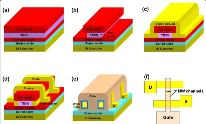
The process flow of the proposed poly-Si NW SONOS memory device is similar to that of the previously reported NW FETs with regard to the NWs formation [10]. First, a dielectric stack consisting of top nitride/tet-raethyl orthosilicate [TEOS] oxide/bottom nitride was sequentially deposited by low-pressure chemical vapor deposition [LPCVD] on a thermally oxidized Si wafer (Figure 1a). After patterning the stack by an anisotropic plasma etching, highly selective lateral etching of the TEOS oxide with diluted hydroflouric acid [HF] solution
was executed to form the nanocavities at the two sides of the stack, as shown in Figure 1b. Then a 100 nm-thickin situ n+-doped poly-Si layer was deposited using SiH4 of 0.49 slm and PH3 of 15 sccm by LPCVD at 600
mtorr and 550°C (Figure 1c). The n+-poly-Si layer was subsequently patterned and anisotropically etched using Cl2/HBr gasses to define the S/D regions and NW
chan-nels to form the JL structure (n+-n+-n+), as illustrated in Figure 1d. It should be noted that the poly-Si embedded in the nanocavities would remain after the anisotropic etching and served as the NW channels. Before gate stack deposition, the top-nitride/bottom-nitride and TEOS oxide layers were removed by hot H3PO4and HF
solution, respectively, to expose the NW channels. Then, a gate dielectric stack of block-oxide/nitride/tun-nel-oxide [ONO] with thicknesses of 12/7/3 nm was deposited by LPCVD. Next, anotherin situ phosphor-ous-doped n+-poly-Si was deposited using SiH4 of 0.49
slm and PH3of 100 sccm by LPCVD and then patterned
to serve as the gate electrode (Figure 1e). After deposit-ing a 500 nm passivation oxide layer, standard metalliza-tion was then performed to complete the device fabrication. Figure 1f shows the schematic top-view lay-out of the device. It should be noted that the nominal
(b)
(a)
(d)
(c)
(e)
(f)
Figure 1 Illustration of the key process steps for fabricating the JL NW SONOS device. (a) A dielectric stack consisting of top nitride/TEOS/ bottom nitride before patterning. (b) Formation of the nano-cavities at the two sides of the stack. (c) Deposition of an n+-doped poly-Si film. (d) Formation of the S/D regions and NW channels by anisotropic dry etching. (e) Final device structure featuring the gate-all-around configuration with an O/N/O gate dielectric stack. (f) Schematic top-view layout of the device.
doping concentrations are 6 × 1020 cm-3and 1 × 1020 cm-3 for the n+-poly-Si gate and the NW channels, respectively. However, it has been reported that the electrical resistivity of a thin film will increase as the dimensions of the film become sufficiently small because the mean free path of conduction carriers in it is reduced [12]. Moreover, owing to the effects of donor deactivation and phosphorous segregation occurring in the Si NW structure [13,14], the effective carrier con-centration in the NW channels practically would be lower than expected. In fact, we have also experimen-tally demonstrated that the resistivity of phosphorous-doped poly-Si NWs increases as NW’s cross-sectional dimensions decrease [15].
Figure 2a shows the top-view scanning electron micro-scopic [SEM] image of a fabricated JL NW device, in which the channel length is defined as the spacing between the S/D regions. The cross-sectional transmis-sion electron microscopic [TEM] image of the NW channel is shown in Figure 2b, indicating that the cross section of the NW is about 11 × 6 nm, which is enclosed by the ONO gate stack and poly-Si gate. Ide-ally, the cross section of the poly-Si NWs is supposed to be rectangular in shape according to the formation scheme of NWs in this work. However, since the NWs experienced a series of wafer cleaning and etching steps conducted in chemical solutions during processing, the NW’s corners were rounded, thus leading to the nearly elliptic profile as observed. In comparison, conventional inversion-mode [IM] memory cells (i.e., n+-i-n+) with undoped poly-Si NW channels having the same ONO stack were also fabricated. In this study, NW memory devices with a channel length of 0.4μm were used for the analyses of electrical and memory characteristics. Results and discussion
In this work, the Fowler-Nordheim [FN] tunneling mechanism was used for the program/erase [P/E] opera-tions of the SONOS memory devices. In the
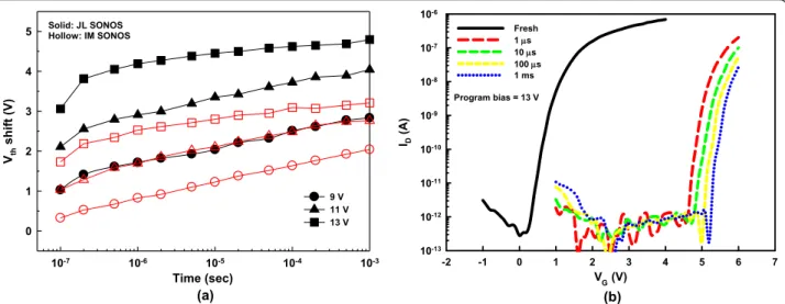
programming process, large positive biases ranging from 9 to 13 V were applied to the gate while keeping the S/ D grounded. Figure 3a presents the programming prop-erties of the JL and IM SONOS memory devices. The JL memory cell apparently exhibits faster programming speed, which could be ascribed to the larger conduc-tion-band carrier concentration in the heavily doped NW channel, thus enhancing the tunneling probability of carrier injection into the nitride trapping layer. With a larger number of electrons tunneling through the tun-nel oxide and getting trapped in the nitride layer, a wider window ofVth shift is resulted. Also note that a
program window up to 4.8 V can be obtained without noticeable degradation of the SS, as revealed in Figure 3b, in which theID-VGcurves in the programmed states
were stressed at 13 V for duration times of 1, 10, 100 μs, and 1 ms, respectively. In contrast, the maximal pro-gram window of the IM memory cell is about 3.2 V with gate bias of 13 V for 1 ms. In addition, the capabil-ity of the large program window of the JL device ensures low voltage operation and multilevel programming with a distinct programmedVthvalue. Figure 4 shows
multi-level programming of the JL device for four states with Vth difference of 1 V between each state. The device
was stressed at 9, 11, and 13 V for 100 ns to the pro-grammed states of 1, 2, and 3, respectively. This result indicates that the JL cell could be placed in one of four discrete states, as described in the inset, to achieve 2 bits/cell storage even with a short duration of 100 ns. This confirms that the abundance of carriers in the JL device lends itself nicely to promoting the programming properties in terms of lower operation voltage, higher speed and larger program window.
In order to study the erase behavior, the cells were firstly programmed to a memory window (ΔVth) of +3
and +2.5 V for the JL and IM devices before erasing, respectively. Negative biases were then applied to the gate with the S/D remained grounded. Figure 5 depicts the erase characteristics of the JL and IM NW SONOS cells. For SONOS CT memory devices, the erase current is composed of electron detrapping and hole injection currents, depending on the band alignment conditions. The slower erasing speed found in the JL device could be attributed to the relatively reduced hole concentra-tion in it. However, it is of interest to note that the dis-parity in erasing speed between the two devices is not as remarkable as that in the programming speed. We speculate that this is due to two factors. For one, the magnitude of FN tunneling current is basically a func-tion of the carrier effective mass and barrier height at SiO2/Si interface [16]. The holes have larger effective
mass and higher potential barrier than the electrons used in the programming process. Hence, the reduced tunneling of holes leads to a less efficient erasing
(a) (b)
Figure 2 SEM and TEM characterization of a fabricated JL poly-Si NW device. (a) Top-view SEM image. (b) Cross-sectional TEM image of the NW channel in (a).
process. Besides, phosphorus impurities tend to segre-gate or be trapped at the surface of Si NW structures, resulting in lower effective density of the carriers at the SiO2/Si NW interface than that in the Si NW bulk [14].
Accordingly, a certain number of holes practically could be induced at the surface of the n+-poly-Si NW chan-nels under erasing operation with large negative gate biases. This, together with the decreased tunneling of holes, may contribute to the smaller disparity in the erasing efficiency between the JL and IM memory cells. Moreover, the erasing speed of the JL device is appar-ently enhanced by increasing the magnitude of the gate bias. Specifically, the JL memory cell displays a compar-ableΔVthof 2.5 V to that of the IM device in 0.2 ms at
-13 V stress. Besides, it also shows that the erase time to achieve the memory window of 3 V is around 5 ms at -13 V, which is very desirable as compared with the recently reported data of poly-Si NW based SONOS memory cells [9,17,18]. On the other hand, a saturation behavior occurs at t = 10-4 sec in the IM SONOS device, and beyond this, the Vth values are found to
slightly go up with a gate bias of -13 V, which may be attributed to the electron injection from the n+-poly-Si gate into the nitride traps at a high electric field. This problem could be relieved by using gate materials with higher work function such as p+-poly-Si, TiN, or TaN relative to the poly-Si channel [19]. Such gate materials are also conducive to obtaining a suitableVthvalue for
heavily doped n+-channel devices by depletion of
(b) (a) VG (V) -2 -1 0 1 2 3 4 5 6 7 ID (A) 10-13 10-12 10-11 10-10 10-9 10-8 10-7 10-6 Fresh 1 Ps 10 Ps 100 Ps 1 ms Program bias = 13 V Time (sec) 10-7 10-6 10-5 10-4 10-3 Vth shi ft (V ) 0 1 2 3 4 5 9 V 11 V 13 V Solid: JL SONOS Hollow: IM SONOS
Figure 3 Programming properties of the JL and IM NW SONOS devices. (a) Programming characteristics at gate biases of 9, 11, and 13 V. (b) Evolution of the ID-VGcurves for the JL device during programming at 13 V from 1μs to 1 ms.
VG (V) -4 -3 -2 -1 0 1 2 3 4 ID ( A ) 10-12 10-11 10-10 10-9 10-8 10-7 10-6 Erase Program bias = 9 V Program bias = 11 V Program bias = 13 V < 1 V 0 (00) > 3 V 3 (11) 2 – 3 V 2 (01) 1 – 2 V 1 (10) Vthrange State
Figure 4ID-VGbehaviors of the JL NW device. ID-VGbehaviors of
the JL NW device for multilevel programming operation with gate biases of 9, 11, and 13 V for 100 ns. Inset shows the definition of Vth
range for each state.
Time (sec) 10-7 10-6 10-5 10-4 10-3 10-2 Vth shift (V) -3 -2 -1 0 -9 V -11 V -13 V Solid: JL SONOS Hollow: IM SONOS
Figure 5 Erase properties of the JL and IM NW SONOS cells. Before erasing, the cells were programmed to Vthshift of +3 V and
carriers owing to the work function difference between the channel and gate material [20].
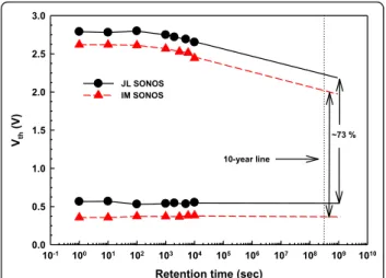
Figure 6 shows the data retention characteristics of the JL and IM NW memory cells at room temperature with programming operation at 11 V for 50μs and eras-ing operation at -10 V for 1 ms. Both devices reveal a charge loss of only 5% at the tested duration time of 104 s, and the extrapolated retention behavior at the end of 10 years that shows 73% of the original P/E window is maintained. Consequently, the almost identical behavior of the charge loss in both devices suggests that the car-rier concentration in the channel does not exert signifi-cant difference on the data retention characteristics. Conclusion
In summary, we have successfully demonstrated the fea-sibility of JL NW SONOS memory device by employing only one in situ-doped n+-poly-Si layer. In addition to the much simplified fabrication process, the fabricated device displays enhanced programming properties and desirable data retention behavior. While no improve-ment in the erasing efficiency is observed, the JL device still exhibits comparable erase window to the IM coun-terpart. Consequently, the proposed JL NW structure with complementary metal-oxide semiconductor compa-tible process appears to be very promising for low-cost and ultrahigh-density NVMs for future 3-D electronics and SOP applications.
Acknowledgements
The authors would like to thank National Nano Device Laboratories and Nano Facility Center of National Chiao Tung University for their assistance in device fabrication. This work was supported in part by the Ministry of Education in Taiwan under Aim for the Top University Program, and in part by the National Science Council of the Republic of China under contract no. 99-2221-E-009-167-MY3.
Author details
1Nano Facility Center, National Chiao Tung University, Hsinchu, 300, Taiwan 2
Department of Electronics Engineering and Institute of Electronics, National Chiao Tung University, Hsinchu, 300, Taiwan3Department of Electrophysics,
National Chiao Tung University, Hsinchu, 300, Taiwan4National Nano Device
Laboratories, 26 Prosperity Road I, Hsinchu, 300, Taiwan Authors’ contributions
CJ designed the study, carried out the SEM and TEM characterization, performed the electrical analysis and drafted the manuscript. TK and TI fabricated the samples and carried out the electrical characterization. HC and TY participated in the design and coordination of the study. All authors read and approved the final manuscript.
Competing interests
The authors declare that they have no competing interests. Received: 30 November 2011 Accepted: 29 February 2012 Published: 29 February 2012
References
1. Kamigaki Y, Minami S, Hagiwara T, Furusawa K, Furuno T, Uchida K, Terasawa M, Yamazaki K: Yield and reliability of MNOS EEPROM products. IEEE J Solid-State Circuits 1989, 24:1714.
2. Lee JD, Hur SH, Choi JD: Effects of floating-gate interference on NAND flash memory cell operation. IEEE Electron Device Lett 2002, 23:264. 3. White MH, Adams DA, Bu J: On the go with SONOS. IEEE Circuits Devices
Mag 2000, 16:22.
4. Khomenkova L, Sahu BS, Slaoui A, Gourbilleau F: Hf-based high-κ materials for Si nanocrystal floating gate memories. Nanoscale Research Lett 2011, 6:172.
5. Sahu BS, Delachat F, Slaoui A, Carrada M, Ferblantier G, Muller D: Effect of annealing treatments on photoluminescence and charge storage mechanism in silicon-rich SiNx:H films. Nanoscale Research Lett 2011, 6:178.
6. Walker AJ, Nallamothu S, Chen EH, Mahajani M, Herner SB, Clark M, Cleeves JM, Dunton SV, Eckert VL, Gu J, Hu S, Knall J, Konevecki M, Petti C, Radigan S, Raghuram U, Vienna J, Vyvoda MA: 3D TFT-SONOS memory cell for ultra-high density file storage applications. VLSI Symp Tech Dig 2003, 2003:29.
7. Lai EK, Lue HT, Hsiao YH, Hsieh JY, Lee SC, Lu CP, Wang SY, Yang LW, Chen KC, Gong J, Hsieh KY, Ku J, Liu R, Lu CY: A highly stackable thin-film transistor (TFT) NAND-type flash memory. VLSI Symp Tech Dig 2006, 2006:46.
8. Lue HT, Hsu TH, Hsiao YH, Hong SP, Wu MT, Hsu FH, Lien NZ, Wang SY, Hsieh JY, Yang LW, Yang T, Chen KC, Hsieh KY, Lu CY: A highly scalable 8-layer 3D vertical-gate (VG) TFT NAND flash using junction-free buried channel BE-SONOS device. VLSI Symp Tech Dig 2010, 2010:131. 9. Hsu HH, Lin HC, Luo CW, Su CJ, Huang TY: Impacts of multiple-gated
configuration on the characteristics of poly-Si nanowire SONOS devices. IEEE Trans. Electron Devices 2011, 58:641.
10. Su CJ, Tsai TI, Liou YL, Lin ZM, Lin HC, Chao TS: Gate-all-around junctionless transistors with heavily doped polysilicon nanowire channels. IEEE Electron Device Lett 2011, 32:561.
11. Colinge JP, Lee CW, Afzalian A, Akhavan ND, Yan R, Ferain I, Razavi P, O’Neill B, Blake A, White M, Kelleher AM, McCarthy B, Murphy R: Nanowire transistors without junctions. Nature Nanotechnol 2010, 5:225. 12. Lacy F: Developing a theoretical relationship between electrical
resistivity, temperature, and film thickness for conductors. Nanoscale Research Lett 2011, 6:636.
13. Björk MT, Schmid H, Knoch J, Riel H, Riess W: Donor deactivation in silicon nanostructures. Nature Nanotechnol 2009, 4:103.
14. Fernández-Serra MV, Adessi C, Blasé X: Surface segregation and backscattering in doped silicon nanowires. Phys Rev Lett 2006, 96:166805. 15. Su CJ, Liou YL, Tsai TI, Lin HC, Huang TY: Fabrication and characterization of junctionless poly-Si nanowire devices with gate-all-around structure. IEEE Silicon Nanoelectronics Workshop 2011, 2011:25.
16. Lenzlinger M, Snow EH: Fowler-Nordheim tunneling into thermally grown SiO2. J Appl Phys 1969, 40:278.
17. Fu J, Jiang Y, Singh N, Zhu CX, Lo GQ, Kwong DL: Polycrystalline Si nanowire SONOS nonvolatile memory cell fabricated on a gate-all-around (GAA) channel architecture. IEEE Electron Device Lett 2009, 30:246. Retention time (sec)
10-1 100 101 102 103 104 105 106 107 108 109 1010 Vth ( V ) 0.0 0.5 1.0 1.5 2.0 2.5 3.0 JL SONOS IM SONOS 10-year line ~73 %
Figure 6 Retention behaviors for the JL and IM NW SONOS devices at room temperature.
18. Hung MF, Wu YC, Tang ZY: High-performance gate-all-around polycrystalline silicon nanowire with silicon nanocrystals nonvolatile memory. Appl Phys Lett 2011, 98:162108.
19. Lee CH, Choi KI, Cho MK, Song YH, Park KC, Kim K: A novel SONOS structure of SiO2/SiN/A12O3with TaN metal gate for multi-giga bit flash
memories. IEDM Tech Dig 2003, 2003:613.
20. Lee CW, Ferain I, Afzalian A, Yan R, Akhavan ND, Razavi P, Colinge JP: Performance estimation of junctionless multigate transistors. Solid-State Electronics 2010, 54:97.
doi:10.1186/1556-276X-7-162
Cite this article as: Su et al.: A junctionless SONOS nonvolatile memory device constructed within situ-doped polycrystalline silicon nanowires. Nanoscale Research Letters 2012 7:162.
Submit your manuscript to a
journal and benefi t from:
7 Convenient online submission 7 Rigorous peer review
7 Immediate publication on acceptance 7 Open access: articles freely available online 7 High visibility within the fi eld
7 Retaining the copyright to your article
![Figure 2a shows the top-view scanning electron micro- micro-scopic [SEM] image of a fabricated JL NW device, in which the channel length is defined as the spacing between the S/D regions](https://thumb-ap.123doks.com/thumbv2/9libinfo/7659534.140278/3.892.86.437.856.1037/figure-scanning-electron-fabricated-channel-defined-spacing-regions.webp)