The effect of oxygen in the annealing ambient on interfacial
reactions of Cu
rTarSi multilayers
Kai-Min Yin
a,U, Li Chang
b, Fu-Rong Chen
a, Ji-Jung Kai
a, Cheng-Cheng Chiang
a,
Peijun Ding
c, Barry Chin
c, Hong Zhang
c, Fusen Chen
ca
Department of Engineering and System Science, National Tsing Hua Uni¨ersity, Hsinchu, Taiwan 300, PR China
b
Department of Materials Science and Engineering, National Chiao Tung Uni¨ersity, Hsinchu, Taiwan 300, PR China
c
Metal Deposition Products Group, Applied Materials, Santa Clara, CA 95054, USA
Received 31 October 1999; received in revised form 15 June 2000
Abstract
Interfacial reactions of CurTarSi multilayers after thermal treatment were investigated using transmission electron micro-scopy. The Cu and Ta films were deposited onto Si wafer by ionized metal plasma technique. The samples were then annealed at 400, 500, 550 and 600⬚C in purified Ar atmosphere for 30 min. The effect of oxygen in the atmosphere on the thermal stability is studied. An interlayer of Ta oxide was observed between Cu and Ta after annealing at 400, 500 and 550⬚C. It is evident that oxygen as residual gas from furnace ambient can diffuse through Cu grain boundaries to form the Ta oxide layer. After annealing at 600⬚C, Si reacted with Ta to form TaSi at the interface of Ta and Si, in the meantime Cu Si with surrounding SiO formed in2 3 2 the Si substrate. The thermal stability of the CurTarSi samples was also examined in a two-step annealing treatment of 400⬚C for 30 min, followed by 600⬚C for 30 min. Even though interlayers of crystalline Ta᎐Cu oxide and Ta silicide were formed, Cu silicides were not observed. Formation of TaO interlayer at the first stage of 400x ⬚C annealing may inhibit Cu diffusion into the Si substrate in the second stage of the 600⬚C annealing process. 䊚 2001 Elsevier Science B.V. All rights reserved.
Keywords: Cu metallization; Diffusion barrier; Oxidation; Transmission electron microscopy
1. Introduction
Cu is the interconnected metal for the next genera-tion ULSI devices because of its lower bulk resistivity w x1 and higher electromigration resistance than Al 2 .w x However, Cu can easily react with Si at a temperature
w x w x
as low as 200⬚C 3 and diffuses fast in SiO 4 under2
electrical field bias, resulting in degradation of device performance. Therefore, a diffusion barrier layer is
needed to prevent Cu from Si and SiO . Tantalum is a2
promising material as a diffusion barrier for Cu metal-lization because Ta and Cu are mutually insoluble w5᎐12 . In addition, Ta has a relative low resistivity inx
the range of 100᎐130 ⍀ cmy1. However, the thermal
UCorresponding author. Tel.:q886-35715131; fax: q886-35720724.
stability of Ta is an important issue for microelectronic fabrication due to its high reactivity with Si at high temperatures. The thermal stability of Ta barrier layer
w x
depends on thickness 5 and temperature. It was re-ported that 50-nm Ta prevents reaction of Cu with Si w x
up to 600⬚C for 30 min in the purified He ambient 8 .
When Cu penetration through the Ta barrier occurs
Y-Cu Si phase and hexagonal-TaSi layer are formed3 2
w x6,8 . The thermal stability of the Ta barrier layer may also depend on the processing ambient. It was found that nitrogen ambient could improve the thermal
w x
stability of Ta up to 700⬚C 8 . The oxygen ambient
enhances the diffusion of Si through the metal layer
and formation of SiO on the top of metal was observed2
w x
in Sirmetal structures 13 . Oxidation of TaSi rSi also2
w x shows similar enhanced diffusion behavior of Si 14 . It was, therefore, thought that oxygen might affect the
0040-6090r01r$ - see front matter 䊚 2001 Elsevier Science B.V. All rights reserved. Ž .
behavior of interfacial reactions for the CurTarSi. The effect of oxygen in ambient for thermal processing
for CurTarSi are seldom reported in the published
literature that may be important for the following processing in ambient-containing oxygen. In this work, we have investigated the effect of oxygen residual from a vacuum furnace on the thermal stability of a 25-nm thick Ta barrier between Cu and Si substrate at various annealing temperatures. Field-emission transmission
Ž .
electron microscopy TEM with X-ray energy
disper-Ž .
sive spectroscopy EDS and electron energy loss
spec-Ž .
troscopy EELS mapping was used for the microstruc-tural and compositional characterization.
2. Experimental
The Cu and Ta films were deposited on 8-inch silicon
wafers in an Applied Materials ElectraTM system that
Ž .
utilized ionized metal plasma IMP processing tech-w x
nology 15 . The base pressure of the IMP chambers
was typically ;10y8 torr. The stacking sequences and
Ž .
thickness of the deposited films were Cu 150 nmrTa
Ž25 nm on Si wafers..
The vacuum furnace using silica tube heated by SiC heating elements was evacuated with a rotary blower pump. Before feeding with Ar gas, the furnace was purged several times with Ar and pumped down to
10y2 torr range. All samples were treated in the
fur-nace at 400, 500, 550 and 600⬚C annealing processes in
Ž .
purified Ar 4 N atmosphere with a pressure of 3 mtorr. The partial pressure of oxygen was estimated to
be approximately 10y3᎐10y4 torr in our experimental
conditions from the result of a leakage test. A two-step
400᎐600⬚C process was also performed. All samples
were cut into 1=1 cm2, before being put into the
furnace. Annealing time at each temperature was 30 w x
min. Wedge method 16 for grinding and polishing was used for cross-sectional TEM specimen preparation. The final step was ion milling to perforation. Mo grids instead of Cu ones were used to mount TEM speci-mens to obtain clean Cu EDS signals from the Cu film in the samples. A JEOL 2010F field emission TEM, equipped with an EDS spectrometer and a Gatan en-ergy filter was used for studying the structures and chemical compositions. Analysis of electron energy loss
Ž .
spectroscopy EELS was performed with the Gatan energy filter.
3. Results and discussion
The microstructure of CurTarSi films in the
as-deposited sample has no interlayer between the films as observed from cross-sectional high-resolution images. The structure of the as-deposited Ta layer is a nano-crystalline beta phase. No texture or preferred orienta-tion of Ta grains can be observed with Si substrate.
After 500⬚C anneal, the typical microstructure of a
CurTarSi sample is shown in Fig. 1a. A 6᎐20-nm thick
interlayer between Cu and Ta layers is clearly observed with uniform gray contrast. A nanobeam diffraction pattern in the inset of Fig. 1a shows that the interlayer is amorphous. The EDS spectrum in Fig. 1b obtained by using a nano-size electron beam indicates that the interlayer contains Ta and O elements. The inverted V shape of the amorphous Ta oxide layer suggests that oxygen from ambient atmosphere may diffuse along grain boundaries of Cu and gradually oxidize Ta. An
Ž
oxygen elemental map in Fig. 1c K-edge 532 eV,
.
energy window width 30 eV obtained by the Gatan energy filter clearly shows the oxygen distribution along a Cu grain boundary. This result is similar to our
previous result from CurTarSiO rSi structure after2
annealing at the same temperature in Ar atmosphere w x in which Ta oxide formed between Ta and Cu 17 . It is noted that the Ta layer remains to be beta phase after
500⬚Cr30 min annealing as the diffraction pattern in
Fig. 1a inset shows. Fig. 2a reveals a triangular region of light contrast in the silicon substrate beneath the
barrier layer from a sample annealed at 550⬚C. Lattice
imaging and nano-diffraction patterns show that it is just pure Si. EDS spectra in Fig. 2b compare the Si
Ž .
peak intensities at 1.74 keV in net counts from the triangular region with those from the adjacent areas in the Si substrate. Depletion of Si mass is, therefore, evident in the triangular region. As a result, Si atoms reacted with the Ta at this temperature to form an amorphous Ta silicide layer, which exhibits dark
con-trast in 2᎐5-nm thick between Ta and Si in Fig. 2a. The
amorphous Ta silicide has been confirmed by both EELS and EDS spectra which show only Ta and Si signals from the layer in Fig. 2c,d. Formation of
amor-phous Ta silicide between Ta and Si at 550⬚C has been
w x
reported 18 . Outdiffusion of Si into Ta is generally w x
found for formation of Ta silicide 19 . Interestingly, it is found that most of the triangular regions are located
around TarTa oxide boundaries roughly below the Cu
grain boundaries where Ta oxide also began to form and is thicker than the rest of the areas. It is most likely that the oxidation of Ta might enhance the Si
andror vacancies migration and Si diffusing along
TarSi interface to form Ta silicide. In this treatment,
no Cu penetration through the TaO and Ta films intox
Si substrate occurred. In addition, EELS data reveals that some Si were dissolved in Ta.
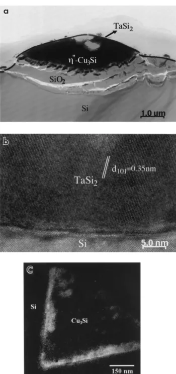
Fig. 3a shows the microstructure of a sample after
600⬚C annealing. A reacted phase surrounded by the
amorphous layer was found in the Si substrate. The reacted phase is Y-Cu Si, which has long period struc-3
ture as analyzed from diffraction patterns and the
surrounding amorphous layer, is identified to be SiO2
by EELS analysis. No metallic Ta and Ta oxide layers
Ž .
Fig. 1. a Cross-sectional TEM image after 500⬚C annealing for 30 Ž .
min. b EDS spectrum of the interlayer between Cu and Ta layers. Ž .c Oxygen map from energy filter.
formed on top of the sample surface as shown in Fig. w x
3a,b. Previous works 6,8 reported similar results for copper silicide formation after treated at room temper-ature.
It is well known that Ta and Cu are mutually insolu-w x
ble 20 . Grain boundary diffusion is probably the path for Cu passing through Ta. Using the diffusion
con-w x
stant of Cu in Ta 8 , the diffusion distance is estimated
to be 6 nm for 30 min at 600⬚C. Therefore, Cu motion
in Ta is quite slow in the temperature range of
400᎐700⬚C. For a 25-nm Ta layer as used in this work,
Cu penetration may not be the only reason to cause the failure. Ta silicide formation as a result of outdiffusion of Si may also have a role. Before oxygen diffusion to
reach Ta at 600⬚C, Cu inward diffusion could occur
while Si outward diffusion started. Vacancies left in the Si depleted regions could provide a strong driving force
for Cu to accelerate into Si to form Cu Si. In the mean3
while, Ta silicide with the presence of Cu would crystal-lize as TaSi .2
In the present study, we believe that mutual diffu-sion of the four major elements Cu, Ta, Si and O with
interfacial reactions among them may occur at 600⬚C.
At 550⬚C oxygen from ambient diffuses through grain
boundaries of Cu to the CurTa interface at which Ta
oxide forms. Once the oxide layer has formed, it may retard diffusion of Cu through Ta layer. Hence, it is apparent that oxygen diffusion is faster than Cu pene-tration into Ta and Si outdiffusion. However, oxygen at
600⬚C is associated only with SiO which is the product2
of oxidation of either Cu Si or TaSi3 2 SiO has been2
w x
shown to be more stable than Ta oxide 21 . It may
explain why Ta oxide is not seen after 600⬚C annealing.
It has been found that Cu penetration precedes and w x
promotes Ta silicide formation 8 . They have reported
that the formation temperature of TaSi2 phase could
w x
be decreased with the presence of Cu 6 . Therefore, with sufficient supply of Si at this temperature, reaction
of Si with Ta to form hexagonal-TaSi phase at 6002 ⬚C
may be possible in our case. Further evidence is shown in our previous work on the thermal stability of
w x
CurTarSiO rSi 17 . It shows that without free silicon2
supply, amorphous Ta oxide can be stable at 600⬚C. No
Ta᎐Si᎐O ternary compound has been predicted from
w x thermodynamic calculation of phase diagram 22 .
Fur-thermore, an oxidation experiment of TaSi2rSi has
shown that the SiO layer formed in dry oxygen am-2
w x bient has the thickness of approximately 7 nm 14 .
w x
Also from a previous report 23 , at equilibrium, the
reaction of Ta oxide with silicon may produce TaSi or2
metallic Ta and SiO . The theoretical phase diagram2
indicates that TaSi can coexist with SiO , but not with2 2
w x
Ta oxide 22 . Therefore, TaSi2 formation could be
more favorable than Ta oxidation at 600⬚C, while Ta
oxide formed at 550⬚C is thought to be possible
be-cause TaSi formation has not occurred.2
Reaction of Si with Cu to form Y-Cu Si phase has3
been shown to take place at low temperature of ap-proximately 200⬚C. The Y-Cu Si phase contains either3
w x high density of stacking faults or vacancies 24 . It has
w x Y
been reported 25,26 that the -Cu Si may catalyze3
the oxidation of Si due to its high density of defects. Oxygen can also diffuse through the reacted layer and
then along the interface of Cu Si3 rSi to form silicon
Fig. 2.
shows formation of oxide at the interface between Si
and Cu Si that the catalyzing process starts, oxidation3
of Cu Si will produce SiO and release free Cu to form3 2
new Cu Si. The process will continuously repeat itself3
until all the Cu is consumed. It is, therefore, believed
that formation of Y-Cu Si may promote penetration3
of Cu through the reacted barrier layer into Si
sub-strate for further growth of Cu silicide. As Cu Si is3
easily oxidized, it may absorb most of oxygen in the
form of SiO , so that TaSi2 2 is prevented from being
oxidized. It has been suggested that Cu could diffuse along grain boundaries in Ta films until it reaches the
Si, then rapidly migrate along the TarSi interface
w x
where Cu Si nucleation sites are encountered 8,12 .3
Recently, we have found some Cu Si precipitates in3
such depleted regions in another study of thermal w x
stability of Ta N barrier between Cu and Si 27 . Hence,2
we speculate that the interface between the depleted regions and the barrier layer could be the nucleation
sites for Cu Si. Further experiments will confirm this3
argument.
In order to realize the effect of Cu diffusion with
interfacial behavior of TarSi interface on thermal
stability, a two-step annealing treatment was carried
out. The treatment consisted of 400⬚Cr30 min
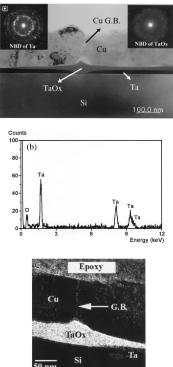
anneal-ing, followed by a 600⬚Cr30 min one. From the 400⬚C
annealing result, a layer of Ta oxide in 4᎐6-nm
thick-ness as shown in Fig. 4a was formed between Cu and Ta due to the strong oxygen affinity of Ta. We expect
that TaO layer could be acted as a strong diffusionx
barrier against Cu penetration, even though its resis-tance may be high for device performance. If the oxide could really inhibit the Cu motion, it is feasible to investigate the interfacial reaction between Ta and Si without Cu interference. Fig. 4b shows a cross-sectional TEM image after the two-step annealing. The mi-crostructure is surprisingly different from that in the
sample only treated with 600⬚C annealing. First, no
copper silicide can be observed, indicating that Cu has not penetrated into Si. Secondly, although there is still
an interlayer approximately 4᎐6-nm thick between the
Cu and Ta layers, the lattice fringes indicate it is a
crystalline phase rather than amorphous TaO . Fromx
EDS and NBD analyses in Fig. 4c,d, the composition of the interlayer consists of Cu, Ta and O and structure has d-spacings in 0.61 and 0.11 nm close to the result of
CurTarSiO rSi multilayers after 600⬚C in a low-2
w x
vacuum condition 17 . The crystalline Ta᎐Cu oxide
layer between Cu and Ta appears to be almost
per-Ž .
Fig. 2. a Cross-sectional TEM image after 550⬚C annealing for 30 Ž .
min. b The EDS spectra obtained from depleted area and the Ž .
adjacent Si substrate. c EDS spectrum obtained from Ta silicide Ž .
indexed in Fig. 2a. d EELS spectrum obtained from Ta Silicide indexed in Fig. 2a.
Ž .
Fig. 3. a Cross-sectional TEM image after 600⬚C annealing for 30
Ž . Ž .
min. b High-resolution TEM image obtained from Ta barrier. c Oxygen elemental map of a Cu Si from another area.3
fectly oriented with long axis perpendicular to the interface. With few grain boundaries observed in the
Ta᎐Cu oxide layer, it could effectively inhibit the Cu
diffusion. The thickness of the oxide did not increase in
the second stage of annealing at 600⬚C, implying no
further oxidation. The thickness of Ta oxide is also
thinner than that in CurTarSiO sample treated at2
the same temperature. In addition, the image contrast
shows that there are two layers between the Ta᎐Cu
oxide and Si substrate. The upper layer with darker contrast is the original Ta whose thickness has been reduced to approximately 17 nm. The gray zone above
Si substrate with thickness of approximately 12᎐17 nm
is identified to be a Ta Si phase as the high-resolution5 3
image at TarSi interface in Fig. 4e shows. This is in
consistence with a previous report that Ta-rich silicide w x
can form at 600⬚C without the presence of Cu 28 . In
general, if the Si is the diffusion species, the metal-rich
silicide phase forms first. In the CurTarSiO sample,2
there is no free silicon supply at 600⬚C, so that silicide formation is unlikely. Formation of Ta-rich phase Ta Si is reported to be possible at 6305 3 ⬚C for 1 h, while
a silicon-rich phase TaSi forms at higher temperature2
w x
approximately 700⬚C for 1 h 28 . Ta Si may be trans-5 3
formed to TaSi with the Cu presence in an early stage2
of annealing.
In the two-stage annealing, the unreacted Ta shows
reaction of Ta with Si at 600⬚C without Cu is slow, in
contrast with the fact that all Ta are in the form of
TaSi when Cu is present. The remaining 17-nm thick2
Ta reduced from the initial 25-nm thickness,
demon-strating that 8-nm thick Ta has consumed for Ta Si5 3
formation. Therefore, it is likely that Si outdiffusion to Ta can reach at least 8-nm distance after 30 min. For
the case of the single stage annealing at 600⬚C, if Cu
could penetrate Ta without oxide in the way, it would have traveled approximately 6 nm according to the calculated diffusion distance. There should have been Ta left if no other mechanism was in operation for Cu and Si reaching each other. Though the mechanism is not actually known as the evidence is insufficient, we suspect that, as mentioned before, vacancies in the Si substrate might be the cause for accelerating Cu pene-tration. Nevertheless, we are unable to explain the action of oxygen, which should diffuse faster than Cu to Ta and Si and why no Ta oxide forms and all oxygen form SiO .2
In the single stage of annealing at 550, Ta oxide can
block Cu penetration, while at 600⬚C the absence of
oxide allows Si react with Cu and Ta to form Cu Si and3
TaSi , so that the barrier stability was destroyed. For2
the two-stage annealing, the amorphous Ta oxide layer
forms at the first stage, which crystallizes as Ta᎐Cu
oxide after reacting with Cu at 600⬚C. If Ta᎐Cu oxide
is stable, Cu has little chance to directly react with silicon to form copper silicide in the second stage annealing. Based on the above observations, it can be concluded that residual gas of oxygen in Ar furnace ambient has a significant effect on the thermal stability of Ta barrier between Cu and Si.
4. Conclusions
The thermal stability of Ta barrier layer in Ar atmo-sphere at various temperatures is summarized as
fol-Ž . Ž . Ž . Fig. 4. a Cross-sectional TEM image after 400⬚C first step annealing. b Cross-sectional TEM image after the two-step annealing 400᎐600⬚C . Ž .c Nano-beam diffraction obtained from the interlayer between Cu and Ta layer. d EDS spectrum of interlayer between Cu and Ta layers. eŽ . Ž . High-resolution TEM image obtained from the interface of Ta layer and Si substrate.
lows. At 500⬚C, oxygen as residual gas from furnace
ambient can diffuse through Cu grain boundaries to Ta
and form TaO layer between Cu and Ta due to thex
strong oxygen affinity of Ta. At 550⬚C, the out-diffusion of silicon becomes noticeable, resulting in a depleted region in Si substrate and formation of amorphous Ta silicide. No Cu silicide formed for samples annealed at
500 and 550⬚C. After 600⬚C annealing, the silicidation
of Ta as TaSi2 and formation of copper silicide with
SiO were observed. No Ta oxide can be seen. For a2
two-step annealing at 400⬚Cr30 min followed by
600⬚Cr30 min, the initially formed TaO layer trans-x
formed into a crystalline Ta᎐Cu oxide in 4᎐6-nm thick
prevented from directly reacting with Si to form Cu Si.3 Meanwhile, the Ta layer reacted with Si to form Ta Si .5 3
References
w x1 H. Takasago, K. Adachi, M. Takada, J. Electron. Mater. 18 Ž1989 319..
w x2 J.R. Lloyd, J.J. Clement, Thin Solid Films 262 1995 135.Ž . w x3 E.R. Weber, Properties of Silicon, The Instituation of
Electri-cal Engineers, London, 1985.
w x4 J.D. McBrayer, R.M. Swanson, T.W. Sigmon, J. Electrochem. Ž .
Soc. 133 1986 1242.
w x5 M.T. Wang, Y.C. Lin, M.C. Chen, J. Electrochem. Soc. 145 Ž1998 2538..
w x6 K. Holloway, P.M. Fryer, Appl. Phys. Lett. 57 1990 1736.Ž . w x7 E. Kolawa, J.S. Chen, J.S. Reid, P.J. Pokela, M.-A. Nicolet, J.
Ž . Appl. Phys. 70 1991 1369.
w x8 K. Holloway, P.M. Fryer, C. Cabral Jr., J.M.E. Harper, P.J. Ž .
Bailey, K.H. Kelleher, J. Appl. Phys. 71 1992 5433.
w x9 P. Catania, J.P. Doyle, J.J. Cuomo, J. Vac. Sci. Technol. A10 Ž1992 3318..
w x10 H. Ono, T. Nakano, T. Ohta, Appl. Phys. Lett. 64 1994 151.Ž . w x11 M. Stavrev, C. Wenzel, A. Moller, K. Drescher, Applied Sur-¨
Ž . face Science 91 1995 257.
w x12 J.S. Kwak, H.K. Baik, J.᎐H. Kim, S.-M. Lee, Appl. Phys. Lett. Ž .
71 1997 2451.
w x13 D. Gupta, ed., Diffusion Phenomena in Thin Films ŽPark .
Ridge, N.J., U.S.A., Noyes Publication 1988 , p. 323.
w x14 S.P. Muraka, D.B. Fraser, W.S. Lindenberger, A.K. Sinha, J. Ž .
Appl. Phys. 51 1980 3241.
w x15 G.A. Dixit, W.Y. Hsu, A.J. Konecni, S. Kirshnan, J.D. Luttrner, R.H. Havemann, J. Forster, G. D. Yao, M. Narasimhan, Z. Xu, S. Ramaswami, F.S. Chen, J. Nulman, IEEE IEDM Tech. Dig. Ž1996 357..
w x16 H. Zhang, Thin Solid Films 320 1998 77.Ž .
w x17 K.-M. Yin, L. Chang, F.-R. Chen, J.J. Kai Unpublished work .Ž . w x18 J.Y. Cheng, L.J. Chen, J. Appl. Phys. 69 1990 2161.Ž .
w x19 H.L. Meyerheim, B. Lengeler, H.E. Goel, J. Appl. Phys. 68 Ž1990 2694..
w x20 T.B. Massalski, ed., Binary Alloy Phase Diagram, AmericanŽ .
Society for Metals, Metals, Park, OH, 1986 , Vol. 1, p. 960. w x21 R. Beyers, R. Sinclair, M.E. Thomas, J. Vac. Sci. Technol. B2
Ž1984 781..
w x22 R. Beyers, J. Appl. Phys. 56 1984 147.Ž .
w x23 K.C. Saraswat, R.S. Nowicki, J.F. Moulder, Appl. Phys. Lett. 41 Ž1982 1127..
w x24 J.K. Solberg, Acta Cryst. A34 1978 684.Ž .
w x25 C.S. Liu, L.J. Chen, J. Appl. Phys 74 9Ž . Ž1993 5501..
w x26 L. Stolt, A. Charai, F.M. D’Heurle, P.M. Fryer, J.M.E. Harper, Ž .
J. Vac. Sci. Technol. A9 1991 1501.
w x27 K.-M. Yin, L. Chang, F.-R. Chen, J.J. Kai Unpublished work .Ž . w x28 A.N. Noya, M. Takeyama, K. Sasaki, E. Aoyagi, K. Hiraga, J.
Ž . Vac. Sci. Technol. A15 1997 253.