IEEE ELECTRON DEVICE LETTERS, VOL. 29, NO. 8, AUGUST 2008 845
High Density and Low Leakage Current in
TiO
2
MIM Capacitors Processed at 300
◦
C
C. H. Cheng, S. H. Lin, K. Y. Jhou, W. J. Chen, C. P. Chou, F. S. Yeh, J. Hu, M. Hwang, T. Arikado,
S. P. McAlister, Senior Member, IEEE, and Albert Chin, Senior Member, IEEE
Abstract—We report Ir/TiO
2/TaN metal–insulator–metal
ca-pacitors processed at only 300
◦C, which show a capacitance
density of 28 fF/µm
2and a leakage current of 3
× 10
−8(25
◦C)
or 6
× 10
−7(125
◦C) A/cm
2at
−1 V. This performance is due
to the combined effects of 300
◦C nanocrystallized high-κ TiO
2,
a high conduction band offset, and high work-function upper
electrode. These devices show potential for integration in future
very-large-scale-integration technologies.
Index Terms—High κ, Ir, metal–insulator–metal (MIM), TiO
2.
I. I
NTRODUCTIONT
HERE is a strong desire to decrease the processing
temperature of metal–insulator–metal (MIM) capacitors
[1]–[16] while maintaining a high capacitance density (ε
0κ/t
κ)
and low leakage current. This requirement is due to the
low-temperature processing associated with low-κ isolation
di-electrics, such as poly-arylene. For very-large-scale-integration
(VLSI) backend integration, temperatures down to 300
◦C may
be desirable [17]. Low-temperature-processed MIM capacitors
would be useful in the integration of future-generation
Ge-on-Insulator (GOI) [18], [19] and IIIV-on-Ge-on-Insulator (IIIVOI) [20]
technologies, where the device performance can crucially be
dependent on the thermal processing budget. Unfortunately,
most high-κ dielectrics, as used for high-density MIM
capaci-tors, require a high process temperature to improve their quality
and increase the κ value by crystallization.
Here, we describe the performance of MIM capacitors
processed at only 300
◦C. A capacitance density of 28 fF/µm
2Manuscript received February 23, 2008. The review of this letter was arranged by Editor A. Z. Wang.
C. H. Cheng and C. P. Chou are with the Department of Mechanical Engineering, National Chiao Tung University, Hsinchu 300, Taiwan, R.O.C. (e-mail: [email protected]; [email protected]).
S. H. Lin and F. S. Yeh are with the Department of Electrical Engineer-ing, National Tsing Hua University, Hsinchu 30013, Taiwan, R.O.C. (e-mail: [email protected]; [email protected]).
K. Y. Jhou is with the Department of Electronics Engineering, National Chiao Tung University, Hsinchu 300, Taiwan, R.O.C. (e-mail: a9368b.ee95g@ nctu.edu.tw).
W. J. Chen is with the Department of Mechanical Materials Engineering, National Yun-Lin Polytechnic Institute, Huwei 632, Taiwan, R.O.C. (e-mail: [email protected]).
J. Hu, M. Hwang, and T. Arikado are with Tokyo Electron Ltd., Tokyo 107-8481, Japan (e-mail: [email protected]; [email protected]; tsunetoshi. [email protected]).
S. P. McAlister is with the National Research Council of Canada, Ottawa, ON K1A 0R6, Canada (e-mail: [email protected]).
A. Chin is with the Department of Electrical Engineering, National Chiao Tung University, Hsinchu 300, Taiwan, R.O.C., and also with the Nano-Electronics Consortium of Taiwan, Hsinchu 30013, Taiwan, R.O.C. (e-mail: [email protected]).
Digital Object Identifier 10.1109/LED.2008.2000833
was obtained with a leakage current of just 3
× 10
−8A/cm
2.
Such capacitor performance compares well with that for
de-vices incorporating 450
◦C processed SrTiO
3(STO) [14], [15]
and is better than that for 400
◦C processed TiTaO [11], [12],
TiLaO [13], and STO [16] capacitors. This was achieved by
using a high-κ TiO
2dielectric that had a high κ value of 65 due
to nanocrystal formation. This occurs at processing
tempera-tures as low as 300
◦C. These MIM capacitors have potential in
analog, RF, and dynamic random access memory applications,
and are vital for GOI [18], [19] and IIIVOI [20] technologies.
II. E
XPERIMENTALP
ROCEDUREThe high-κ TiO
2MIM capacitors were fabricated on
stan-dard Si wafers having a 2-µm-thick SiO
2isolation layer on
the Si substrates. Then, TaN (50 nm thick) was deposited on a
200-nm Ta layer and used as the lower capacitor electrode. The
TaN surface was first given an NH
3plasma treatment [13]–[16]
and then exposed to an O
2plasma—this being done to increase
the oxidation resistance before the high-κ dielectric deposition
and postdeposition anneal (PDA). Then, a 20-nm-thick TiO
2dielectric was deposited at room temperature by electron-beam
evaporation at a pressure of 2
× 10
−6torr followed by a 300
◦C
PDA for 10 min in an oxygen ambient of 1-atm pressure.
Finally, a 20-nm Ir layer was deposited and patterned to form
the top electrode. The capacitors were 180 µm
× 180 µm in
size, thus minimizing any complications from variations in
dimensions arising from lithography. The fabricated devices
were characterized by standard C–V and J –V measurements.
III. R
ESULTS ANDD
ISCUSSIONIn Fig. 1(a) and (b), we show the C–V and J –V
characteris-tics of Ir/TiO
2/TaN capacitors, respectively. A high capacitance
density of 28 fF/µm
2was measured along with a low leakage
current of 3
× 10
−8A/cm
2at
−1 V. These results are compared
with other MIM data in Table I. Our results are an improvement
over those for a Ni/STO/TaN device, which had a slightly lower
density of 25 fF/µm
2and were processed at 400
◦C [16]. Since
the work function of the Ni electrode is only slightly lower
than Ir, the better leakage in the Ir/TiO
2/TaN device, when
compared with Ni/STO/TaN, is due to the larger conduction
band offset (∆E
C) of TiO
2with respect to the STO [21], [22].
This is because the larger ∆E
Cand the higher work-function
electrode will form a higher Schottky barrier height to lower
the leakage current by Schottky emission mechanism [15], [16].
A larger ∆E
Cto the metal electrode is also important for the
high-temperature leakage current at 125
◦C. We found a 125
◦C
0741-3106/$25.00 © 2008 IEEE846 IEEE ELECTRON DEVICE LETTERS, VOL. 29, NO. 8, AUGUST 2008
Fig. 1. (a) C–V and (b) J –V (measured at 25◦C and 125◦C) characteristics for Ir/TiO2/TaN capacitors.
leakage current of 6
× 10
−7A/cm
2measured at
−1 V. This
is, to the best of our knowledge, better than previous data
and is at a high capacitance density of 28 fF/µm
2[1]–[16].
In addition, a small loss tangent of 0.013 is obtained at such
large 28 fF/µm
2density using the advanced four-element
model and two-frequency calculation [23], which can be
de-creased with decreasing capacitance density [24]. A quadratic
voltage coefficient of capacitance (α) of 5010 ppm/V
2was
obtained at 500 kHz, which can also rapidly be improved with a
decreased capacitance density [14] used for analog/RF
applica-tion. A temperature coefficient of capacitance of 353 ppm/
◦C
was measured even at a high 28 fF/µm
2density.
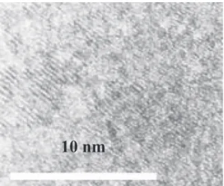
To understand the performance improvements, we examined
the 300
◦C processed TiO
2structure by cross-sectional TEM.
As shown in Fig. 2, the nanocrystallization of TiO
2is
observ-able even at 300
◦C. This nanocrystallization effect yields a
high κ value of
∼65 for the TiO
2dielectric and explains why
the leakage current is better than that for previous TiTaO [11],
[12] and TiLaO [13] MIM capacitors, shown in Table I, which
have a κ value of 45. The high κ value, in combination with
∆E
Cand the high work-function Ir electrode, helps explain the
Fig. 2. Cross-sectional TEM image of a TiO2sample after 300◦C processing.
TABLE I
COMPARISON OFMIM CAPACITORSTHATHAVEVARIOUS DIELECTRICS ANDMETALELECTRODES
good 125
◦C leakage current. This is because the larger ∆E
Cvalue lowers the Schottky emission current, and the high κ
value decreases the conducting electric field for both Schottky
emission and Frenkel–Pool mechanism [15].
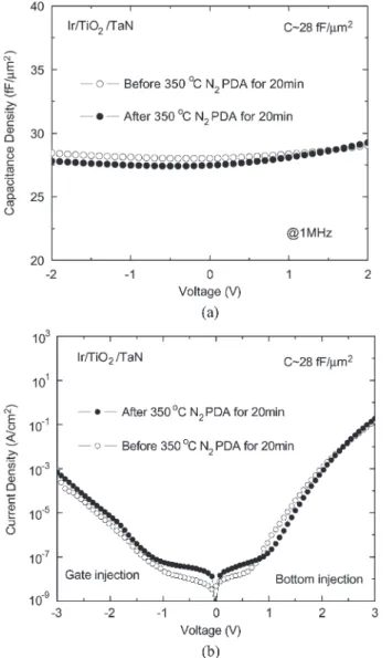
To study the thermal stability, we annealed an Ir/TiO
2/TaN
capacitor at 350
◦C for 20 min under an N
2ambient. In
Fig. 3(a) and (b), we display the C–V and J –V characteristics
before and after this thermal treatment. Only a small
degrada-tion of the capacitance density and leakage current occurred,
indicating the good thermal stability of both the top Ir electrode
and the metal-electrodes-capped TiO
2. We also note that good
thermal stability has been reported for Ir/HfAlON pMOS even
at rapid thermal annealing temperatures of up to 900
◦C [25].
IV. C
ONCLUSIONWe have demonstrated Ir/TiO
2/TaN MIM capacitors with a
capacitance density of 28 fF/µm
2along with a leakage current
of 3
× 10
−8A/cm
2at
−1 V. Since the device processing was
performed at 300
◦C, this would permit these capacitors to be
integrated into a VLSI backend, along with advanced low-κ
isolation dielectrics, or with future front-end GOI and IIIVOI
technologies.
CHENG et al.: HIGH DENSITY AND LOW LEAKAGE CURRENT IN TiO2MIM CAPACITORS 847
Fig. 3. Thermal stability behavior of a 300◦C formed Ir/TiO2/TaN capacitor
after a 350◦C N2anneal for 20 min.
A
CKNOWLEDGMENTThe National Chiao Tung University (NCTU) team would
like to thank the support from Tokyo Electron Ltd. and NSC
(95-2221-E-009-298-MY3).
R
EFERENCES[1] C.-M. Hung, Y.-C. Ho, I.-C. Wu, and K. O, “High-Q capacitors im-plemented in a CMOS process for low-power wireless applications,” in
Proc. IEEE MTT-S Int. Microw. Symp. Dig., 1998, pp. 505–511.
[2] J. A. Babcock, S. G. Balster, A. Pinto, C. Dirnecker, P. Steinmann, R. Jumpertz, and B. El-Kareh, “Analog characteristics of metal–insulator– metal capacitors using PECVD nitride dielectrics,” IEEE Electron Device
Lett., vol. 22, no. 5, pp. 230–232, May 2001.
[3] C. H. Ng, K. W. Chew, and S. F. Chu, “Characterization and compari-son of PECVD silicon nitride and silicon oxynitride dielectric for MIM capacitors,” IEEE Electron Device Lett., vol. 24, no. 8, pp. 506–508, Aug. 2003.
[4] T. Ishikawa, D. Kodama, Y. Matsui, M. Hiratani, T. Furusawa, and D. Hisamoto, “High-capacitance Cu/Ta2O5/Cu MIM structure for SoC
applications featuring a single-mask add-on process,” in IEDM Tech. Dig., 2002, pp. 940–942.
[5] S. B. Chen, J. H. Lai, A. Chin, J. C. Hsieh, and J. Liu, “High density MIM capacitors using Al2O3and AlTiOxdielectrics,” IEEE Electron Device
Lett., vol. 23, no. 4, pp. 185–187, Apr. 2002.
[6] S. B. Chen, J. H. Lai, K. T. Chan, A. Chin, J. C. Hsieh, and J. Liu, “Frequency-dependent capacitance reduction in high-k AlTiOxand
Al2O3 gate dielectrics from IF to RF frequency range,” IEEE Electron
Device Lett., vol. 23, no. 4, pp. 203–205, Apr. 2002.
[7] X. Yu, C. Zhu, H. Hu, A. Chin, M. F. Li, B. J. Cho, D.-L. Kwong, P. D. Foo, and M. B. Yu, “A high-density MIM capacitor (13 fF/µm2) using ALD HfO2dielectrics,” IEEE Electron Device Lett., vol. 24, no. 2,
pp. 63–65, Feb. 2003.
[8] H. Hu, S. J. Ding, H. F. Lim, C. Zhu, M. F. Li, S. J. Kim, X. F. Yu, J. H. Chen, Y. F. Yong, B. J. Cho, D. S. H. Chan, S. C. Rustagi, M. B. Yu, C. H. Tung, A. Du, D. My, P. D. Fu, A. Chin, and D. L. Kwong, “High performance HfO2− Al2O3 laminate MIM capacitors by ALD
for RF and mixed signal IC applications,” in IEDM Tech. Dig., 2003, pp. 379–382.
[9] S. J. Kim, B. J. Cho, M.-F. Li, C. Zhu, A. Chin, and D. L. Kwong, “HfO2 and lanthanide-doped HfO2 MIM capacitors for RF/mixed IC
applications,” in VLSI Symp. Tech. Dig., 2003, pp. 77–78.
[10] S. J. Kim, B. J. Cho, M. B. Yu, M.-F. Li, Y.-Z. Xiong, C. Zhu, A. Chin, and D. L. Kwong, “High capacitance density (> 17 fF/µm2) Nb
2O5–based
MIM capacitors for future RF IC applications,” in VLSI Symp. Tech. Dig., 2005, pp. 56–57.
[11] K. C. Chiang, A. Chin, C. H. Lai, W. J. Chen, C. F. Cheng, B. F. Hung, and C. C. Liao, “Very high-κ and high density TiTaO MIM capacitors for analog and RF applications,” in VLSI Symp. Tech. Dig., 2005, pp. 62–63. [12] K. C. Chiang, C. H. Lai, A. Chin, T. J. Wang, H. F. Chiu, J. R. Chen,
S. P. McAlister, and C. C. Chi, “Very high density (23 fF/µm2) RF MIM capacitors using high-κ TiTaO as the dielectric,” IEEE Electron Device
Lett., vol. 26, no. 10, pp. 728–730, Oct. 2005.
[13] C. H. Cheng, H. C. Pan, H. J. Yang, C. N. Hsiao, C. P. Chou, S. P. McAlister, and A. Chin, “Improved high-temperature leakage in high-density MIM capacitors by using a TiLaO dielectric and an Ir electrode,” IEEE Electron Device Lett., vol. 28, no. 12, pp. 1095–1097, Dec. 2007.
[14] K. C. Chiang, C. C. Huang, A. Chin, W. J. Chen, H. L. Kao, M. Hong, and J. Kwo, “High performance micro-crystallized TaN/SrTiO3/TaN
ca-pacitors for analog and RF applications,” in VLSI Symp. Tech. Dig., 2006, pp. 126–127.
[15] K. C. Chiang, C. C. Huang, A. Chin, H. L. Kao, G. L. Chen, W. J. Chen, Y. H. Wu, and S. P. McAlister, “High-performance SrTiO3
metal–insulator–metal capacitors for analog applications,” IEEE Trans.
Electron Devices, vol. 53, no. 9, pp. 2312–2319, Sep. 2006.
[16] K. C. Chiang, C. H. Cheng, H. C. Pan, C. N. Hsiao, C. P. Chou, A. Chin, and H. L. Hwang, “High-temperature leakage improvement in metal–insulator–metal capacitors by work-function tuning,” IEEE
Elec-tron Device Lett., vol. 28, no. 3, pp. 235–237, Mar. 2007.
[17] Y. Ohoka, K. Inoue, T. Hayashi, N. Komai, S. Arakawa, R. Kanamura, and S. Kadomura, “Integration of self-formed barrier technology for 32 nm-node Cu dual-damascene interconnects with hybrid low-k (Par/SiOC) structure,” in VLSI Symp. Tech. Dig., 2006, pp. 114–115. [18] C. H. Huang, M. Y. Yang, A. Chin, W. J. Chen, C. X. Zhu, B. J. Cho,
M.-F. Li, and D. L. Kwong, “Very low defects and high performance Ge-On-Insulator p-MOSFETs with Al2O3 gate dielectrics,” in VLSI
Symp. Tech. Dig., 2003, pp. 119–120.
[19] D. S. Yu, C. H. Huang, A. Chin, C. Zhu, M. F. Li, B. J. Cho, and D. L. Kwong, “Al2O3/Ge-on-insulator n- and p-MOSFETs with fully
NiSi and NiGe dual gates,” IEEE Electron Device Lett., vol. 25, no. 3, pp. 138–140, Mar. 2004.
[20] C. C. Liao, S. Kao, A. Chin, D. S. Yu, M.-F. Li, C. Zhu, and S. P. McAlister, “Comparing high mobility InGaAs FETs with Si and GOI devices,” in Proc. 64th DRC, 2006, pp. 85–86.
[21] J. Robertson, “Band offsets of wide-band-gap oxides and implications for future electron devices,” J. Vac. Sci. Technol. B, Microelectron. Process.
Phenom., vol. 18, no. 3, pp. 1785–1791, May 2000.
[22] S. A. Campbell, D. C. Gilmer, X. C. Wang, M.-T. Hsieh, H.-S. Kim, W. L. Gladfelter, and J. Yan, “MOSFET transistors fabricated with high permitivity TiO2 dielectrics,” IEEE Trans. Electron Devices, vol. 44,
no. 1, pp. 104–109, Jan. 1997.
[23] H. T. Lue, C. Y. Liu, and T. Y. Tseng, “An improved two-frequency method of capacitance measurement for SrTiO3as high-κ gate dielectric,”
IEEE Electron Device Lett., vol. 23, no. 9, pp. 553–555, Sep. 2002.
[24] H. C. Li, W. Si, A. D. West, and X. X. Xia, “Thickness dependence of dielectric loss in SrTiO3 thin films,” Appl. Phys. Lett., vol. 73, no. 4,
pp. 464–466, Jul. 27, 1998.
[25] D. S. Yu, A. Chin, C. H. Wu, M.-F. Li, C. Zhu, S. J. Wang, W. J. Yoo, B. F. Hung, and S. P. McAlister, “Lanthanide and Ir-based dual metal-gate/HfAlON CMOS with large work-function difference,” in