國
立
交
通
大
學
奈米科技研究所
碩
士
論
文
鋯鈦酸鉛薄膜之微波水熱式退火
並應用於感測器
Hydrothermal Annealing of PZT Thin Film with
Microwave System and Sensor Application
研 究 生:徐乙介
學 號:9352511
指導教授:柯富祥 博士
劉增豐 博士
鋯鈦酸鉛薄膜之微波水熱式退火並應用於感測器
Hydrothermal Annealing of PZT Thin film with Microwave System
and Sensor Application
研 究 生:徐乙介 Student:Yi-Chieh Hsu 指導教授:柯富祥 Advisor:Fu-Hsiang Ko 劉增豐 Tzeng-Feng Liu 國 立 交 通 大 學 奈 米 科 技 研 究 所 碩 士 論 文 A Thesis
Submitted to Institute of Nanotechnology College of Engineering
National Chiao Tung University in partial Fulfillment of the Requirements
for the Degree of Master
in
Nanotechnology
June 2006
Hsinchu, Taiwan, Republic of China
鋯鈦酸鉛薄膜之微波水熱式退火並應用於感測器
國立交通大學奈米科技研究所
學生:徐 乙 介 指導教授:柯 富 祥 博士
劉 增 豐 博士
摘要
石英晶體微天秤(Quartz Crystal Microbalance)技術已經發展成熟,並 廣泛應用在微小質量的偵測上,根據Sauerbrey方程式,若將QCM感測面 積變小或提高感測器的振盪頻率,則可以提高其靈敏度,但是石英不易加 工,在製程處理上受限制。本研究則是利用同樣具有壓電性質的材料鋯鈦 酸鉛(PbZrxTi1-xO3),以溶膠-凝膠法(Sol-gel)製成壓電薄膜,來取代傳統 的石英晶體;再以微波反應系統進行水熱式退火,來取代傳統高溫製程上 的熱處理方式,同時根據實驗結果,進一步推論水熱式退火的反應機制。 再利用掃描式電子顯微鏡 (SEM)、原子力顯微鏡 (AFM)、 X光繞射儀 (XRD)…等,去討論在不同參數下PZT薄膜的性質,並以實驗所得之最佳 參數,以半導體微影技術製成PZT薄膜感測器。另者,利用發展出的感測 器對揮發性的有機物之蒸氣進行偵測,其振盪頻率約為30MHz,偵測極限 約為1ppm。
Hydrothermal Annealing of PZT Thin Film with
Microwave System and Sensor Application
Institute of Nanotechnology National Chiao Tung University
Student: Yi-Chieh Hsu Advisor: Fu-Hsiang Ko Tzeng-Feng Liu
Abstract
QCM (Quartz Crystal Microbalance) has been received widely attraction for the application in the measurement of minute masses. According to the prediction of Sauerbrey equation, the sensitivity will be improved when the surface area is decreased or the resonance frequency of the unloaded resonator is increased. However, it is difficult for the quartz substrate to scale-down by photolithography. In this article, we develop another type of piezoelectric material, PbZrxTi(1-x)O3 (PZT), as a thin film by sol-gel route to replace the
quartz crystal as a resonator. The novel hydrothermal annealing with microwave system is proposed to substitute the conventional furnace annealing. We also propose a reasonable mechanism for the hydrothermal annealing base on the experimental results. The films with different recipe of the treatments are analyzed by SEM, AFM, XRD and EDS. In addition, the films with good quality are applied to sense the vapor of volatile chemicals. The resonant frequency of the developed PZT sensor is about 30MHz and the sensing limit is estimated to about 1ppm.
Acknowledgement 非常感謝指導教授 柯富祥 博士 在生活上及實驗論文方面的細心教 誨及指導,也感謝 黃國華 教授 的建議與指導,使我在這兩年的碩士生 涯裡獲益良多。同時感謝孟德學長在頻率量測及分析上的大力相助,才能 讓此論文更臻完整。 感謝其昌學長、俊淇學長在實驗及口試準備上的指導與建議,感謝佳 慧學姊、文宏學長、人豪學長、峻銘學長、界佐學長、光電所家揚學長在 研究經驗和技術的傳承,感謝嘉偉學弟、交大材料所同學志偉、其慶在光 學微影上給予的協助,感謝清大材料所同學德銘在 XRD 及 EDS 的分析上的 大力幫忙,也感謝坤霖、建文、佳典、志威、昇成、英儒、士紋、昱勳、 維揚、宜輝、大鈞在課業、實驗及生活上的勉勵和照應,感謝學弟妹群芳、 亦儂、志杰、敬雅的支持與祝福。在碩士班這兩年來酸甜苦辣點滴於心, 然而需要感謝的人實在太多了,在此一併致謝。 最後深深感謝我的爸爸、媽媽、阿嬤、弟弟士卜、女朋友佩瑩,感謝 你們全心全意的支持及生活的照顧,在此將這份小小的榮耀獻給你們。
Content Chinese Abstract ………...Ⅰ English Abstract ……….…...Ⅱ Acknowledgement ………...Ⅲ Content ……….Ⅳ List of Tables ………...Ⅵ List of Figures ………..Ⅶ Chapter 1 Introduction ………...1 1.1 General Introduction………..1 1.2 QCM ………..2 1.3 PZT ………....6
Chapter 2 Literatures Review ………..10
2.1 The Fabrications of PZT Thin Films………10
2.1.1 MOCVD ...10
2.1.2 Magnetron Sputtering Deposition ……….……11
2.1.3 Sol-gel and RTA Annealing ………..11
2.1.4 PLD (Pulsed Laser Deposition)………..12
2.1.5 DPF (Dense Plasma Focus)………...…….12
2.2 Hydrothermal Annealing ………...…………..13
2.3 Microwave System ………..15
2.4 The PZT Resonant Piezo-Layer Sensor ……….….19
2.5 Motivation ………...21
Chapter 3 Experiments ……….22
3.1 Process of PZT Thin Films ………..22
3.2 Process of PZT Sensors ………...27
4.1 The Mechanism of Hydrothermal Annealing ………..29
4.2 Characterization of PZT Thin Films …………..……….30
4-2.1 SEM Analysis ….………...30
4-2.2 AFM Analysis ….………...37
4-2.3 XRD Analysis ….………...41
4-2.4 EDS Analysis ….………...44
4.3 Application of PZT Sensors for Chemical Analysis …………...45
4-2.1 The Qualitative Analysis by PZT Sensors ……….46
4-2.2 The Quantitative Analysis by PZT sensors ……….…..48
Chapter 5 Conclusions ……….55
List of Tables
Table 2-1 The fabrication of PZT thin film ………...14 Table 2-2 The dissipation factor of several materials ………..17 Table 4-1 The analysis of PZT thin films by EDS with hydrothermal
List of Figures
Fig.1-1 Schematic of a typical QCM ……….…....2
Fig.1-2 The assignment of axes to a quartz crystal ……….….…..3
Fig.1-3 The specific orientation of the quartz crystal plate with respect to the crystal axes ……….………..……3
Fig.1-4 The different orientation of the quartz crystal plate with respect to temperature ……….….…….4
Fig.1-5 The crystal structure of ABO3 ……….…..6
Fig.1-6 The crystal structure of PZT (a) over and (b) under TC ………7
Fig.1-7 The morphotropic boundary depends on the temperature and composition of PZT ……….………...8
Fig.1-8 The cell parameter of PZT with respect of composition ………...8
Fig. 2-1 The electromagnetic spectrum ………...15
Fig. 2-2 The dipole rotation ……….17
Fig. 2-3 Molecules try to align to the microwave field ………...17
Fig. 2-4 Conductive heating ………18
Fig. 2-5 Microwave heating ……….18
Fig. 2-6 Structure of a RPL ………..19
Fig. 2-7 RPL array ………...19
Fig. 2-8 Me-Cav ……….……….….20
Fig. 2-9 Qx-Cav ………...20
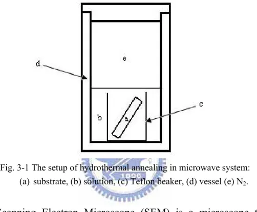
Fig. 3-1 The setup of hydrothermal annealing in microwave system ………..23
(a) substrate, (b) solution, (c) Teflon beaker, (d) vessel (e) N2 Fig. 3-2 The working illustration of AFM ………...24
Fig. 4-1 The PZT film after hydrothermal annealing:
the film might be lost while contacting with the precipitation of the solution ………..……….29 Fig. 4-2 The SEM micrographs of PZT thin film with hydrothermal
annealing ………31 (a) before annealing, (b) KOH=0.5M, Pb(NO3)2=0.1M, (c)
KOH=0.5M, Pb(NO3)2=0.15M, (d) KOH=0.5M, Pb(NO3)2=0.2M, (e)
KOH=1M, Pb(NO3)2=0.05M, (f) KOH=1M, Pb(NO3)2=0.1M, (g)
KOH=1M, Pb(NO3)2=0.15M, (h) KOH=1M, Pb(NO3)2=0.2M, (i)
KOH=2M, Pb(NO3)2=0.05M, (j) KOH=2M, Pb(NO3)2=0.1M, (k)
KOH=2M, Pb(NO3)2=0.15M, (l) KOH=2M, Pb(NO3)2=0.2M
Fig. 4-3 The AFM micrographs of PZT thin film with hydrothermal
annealing ………38 (a) before annealing, (b)KOH=0.5M, Pb(NO3)2=0.1M, (c)
KOH=0.5M, Pb(NO3)2=0.15M, (d) KOH=0.5M, Pb(NO3)2=0.2M, (e)
KOH=1M, Pb(NO3)2=0.1M, (f) KOH=1M, Pb(NO3)2=0.15M, (g)
KOH=1M, Pb(NO3)2=0.2M, (h) KOH=2M, Pb(NO3)2=0.15M, (i)
KOH=2M, Pb(NO3)2=0.2M
Fig. 4-4 The XRD patterns of PZT thin films with hydrothermal
annealing ………42 (a) KOH=0.5M, (b) KOH=1M, (c) KOH=2M
Fig. 4-5 The top view of a PZT sensor ………45 Fig. 4-6 The shift frequency of a PZT sensor ………..46
(a) The spray of alcohol, (b) The spray of acetone, (c) The spray of toluene
(a) by vapor of alcohol at 30℃, (b) by vapor of alcohol at 40℃, (c) by vapor of alcohol at 50℃, (d) by vapor of alcohol at 60℃
Fig. 4-8 The shifted frequency of a PZT sensor ………..51 (a) by vapor of toluene at 30℃, (b) by vapor of toluene at 40℃, (c) by vapor of toluene at 50℃, (d) by vapor of toluene at 60℃
Fig. 4-9 The shift frequency of a PZT sensor with the vapor pressure ………54 (a) alcohol, (b) toluene
Chapter 1 Introduction
1-1 General Introduction [1]
Piezoelectricity is a phenomenon exhibited by noncentrosymmetric crystals whereby an electric polarization (i.e. charge) is induced in the material upon the application of a stress. Conversely, it is the development of an induced strain which is directly proportional to an applied electric. The latter phenomenon is known as the converse effect and is utilized in actuation. The former is called the direct effect and is used in sensing dynamic pressure changes, changes in acceleration (from shock or vibration), and changes in force. Whether a material that belongs to one of the piezoelectric point groups actually exhibits measurable piezoelectricity has to be measured experimentally.
Through proper design and selection of materials, the frequency range that piezoelectric materials can detect changes in force or motion can range from below 1Hz to above several MHz. Displacements in the mm range can be precisely measured as can force changes from mN to kN. The rugged solid-state construction of industrial piezoelectric ceramic sensors enables them to operate under most harsh environmental conditions, including dirt, oil, and most chemical atmospheres. They perform well over a wide temperature range and resist damage from severe shock and/or vibration. Piezoelectricity exists in some naturally occurring crystals such as quartz. However, the bulk of the piezoelectric materials used for commercial sensing applications come from synthetic polycrystalline ferroelectric ceramics, such as PZT. Compared to single crystals ceramics offer the advantage of high strength and ease of fabrication in general, especially into complex shapes and large area pieces.
1-2 Quartz Crystal Microbalance (QCM)
Quartz crystal resonators have seen wide application in the measurement of small masses due to their stability, simplicity of measurement, high precision, high sensitivity, and ease of analysis. Numerous literatures report the mass change with respect to the frequency shift forms the basic of QCM resonators.
The theoretical foundation for the use of piezoelectricity was first proposed by Raleigh (1885), but the first thorough investigation was by Jacques and Pierre Curie in 1880 (Curie and Curie, 1880). A quartz crystal microbalance (QCM) consists of a thin quartz disk with electrodes plated on it as can be seen in Fig. 1-1.[2]
Fig.1-1 Schematic diagram of a typical QCM.
A piezoelectric quartz crystal resonator is a precisely cut slab from a natural or synthetic crystal of quartz. Quartz crystal in its perfect natural form can be seen in Fig. 1-2.[2]
Fig.1-2 The assignment of axes to a quartz crystal.
As the QCM is piezoelectric, an oscillating electric field applied across the device induces an acoustic wave that propagates through the crystal and meets minimum impedance when the thickness of the device is a multiple of a half wavelength of the acoustic wave. A QCM is a shear mode device in which the acoustic wave propagates in a direction perpendicular to the crystal surface (Ebersole et al., 1990). To make this happen, the quartz crystal plate must be cut to a specific orientation shown in Fig. 1-3 with respect to the crystal axes.[2]
Fig.1-3 The specific orientation of the quartz crystal plate with respect to the crystal axes.
A resonant oscillation is achieved by adopting the crystal into an oscillation circuit where the electric and the mechanical oscillations are near to the fundamental frequency of the crystal. The fundamental frequency depends upon the thickness of the wafer, its chemical structure, its shape and its mass. Some factors can influence the oscillation frequency, like the temperature, the thickness, the density and the shear modulus of the quartz. Fig. 1-4 shows the different orientations of QCM with respect to temperatures. It can be seen that the frequency of the AT-cut is more stable than other modes near the room temperature, and this is the reason that the common QCM is made in AT-cut.[3]
Fig.1-4 The different orientations of the quartz crystal plate with respect to temperatures.
The principle of operation as a balance is that any mass added to, or removed from, the electrode(s) induces a frequency shift, ∆f, related to the mass change ∆m. The high inherent sensitivity (<l ng/cm2) derives from the high resolution with which even very small frequency changes can be measured.
Sauerbrey first provided a description and experimental verification of the mass/frequency relationship between rigid foreign layers firmly attached to the quartz crystal resonators in 1959. The frequency change is directly proportional to the added mass as long as the added mass behaves elastically similar to the quartz itself as shown in eq. (1)
(1)
where ∆f is the change in the resonance frequency due to the added mass, fro is
the resonance frequency of the unloaded resonator, ρq and Gq are the density
and shear modulus of the quartz, and A is the surface area of the resonator.[4] The mass uptake of moisture into the films was measured using a quartz crystal microbalance (QCM) with dissipation (QCM-D). The QCM-D technique has been described previously in the literature.[5] The QCM-D is a transient mode resonator that measures the frequency and the dissipation of the crystal simultaneously. The dissipation factor, D, is the reciprocal of the Q factor and defined as
(2)
where Edissipated is the energy dissipated during one period of oscillation, and
Estored is the energy stored in the oscillating system. A typical 10 MHz, AT-cut
quartz crystal working in a vacuum or gaseous environment has a dissipation factor in the range 10-6 –10-4.[6]
1-2 PZT
Due to the ferroelectric and piezoelectric properties, solid solutions of Pb(Zr, Ti)O3 have been used in many applications in microelectronics. It was
in the 1950s that the ferroelectric characteristic of PZT was first observed in Japan. Solid solutions of PbZrxTi(1−x)O3 crystallize in the perovskite structure
wrote in ABO3. Figure 1-5 shows the crystal structure of ABO3 where A is the
larger cations sited in corner of the cubic, O is atoms of oxygen sited in face-center, and B is the smaller cation sited in body-center. It can also be presented in BO6 octahedral-like structure where A is sited in the body-center
of B atoms.[7]
Fig.1-5 The crystal structure of ABO3.
Perovskite-like oxides have been at the center of research on ferroelectric and piezoelectric materials for the past fifty years because of their simple cubic structure at high temperatures and the variety of high symmetry phases with polar states found at lower temperatures. Among these materials the ferroelectric PbZrxTi(1-x)O3 (PZT) solid solutions have attracted special
attention since they exhibit an unusual phase boundary which divides regions with rhombohedral and tetragonal structures, called the morphotropic phase boundary (MPB).[8]
At the Curie temperature (TC), the point symmetry formed by Ti/Zr-ions
and oxygen changes from a symmetric cubic state to an asymmetric ferroelectric state because of a displacement of the titanium or zirconium ions of about 0.1 Å. Figure 1-6 indicates the crystal structure.[9]
Fig.1-6 The crystal structure of PZT (a) over and (b) under TC.
It is possible to make compositions of PZT, which is near a MPB between two different solid phases. These phases can coexist in a very wide temperature range. The different possible states are a tetragonal and a rhombohedral state which are preferred by Ti and Zr, respectively. How much of the PZT that will be in the respective tetragonal state and the rhombohedral state respectively, depends on the composition. By using different amounts of titanium or zirconium, it is possible to change the structure and properties of PZT, which can be seen in Fig.1-7 and Fig.1-8.[10] The importance of a phase boundary, when poling, was realized by Jaffe in 1954 and since then, PZT has been used in many technical applications. Recently, another feature of the morphotropic phase boundary has been revealed by the discovery of a ferroelectric monoclinic phase in the PbZrxTi(1-x)O3 ceramic system. From a
synchrotron x-ray powder diffraction study of a composition with x=0.48, a tetragonal-to- monoclinic phase transition was discovered at ~300 K.
Fig.1-7 The morphotropic boundary depends on the temperature and composition of PZT.
The strong response on poling in such compositions of PZT is the explanation to why it is used when making sensitive transducers. Strong poling response will give sensitive sensors. In PZT transducers direct and converse piezoelectric effects are commonly used. In sensors, the direct effect transforms electric polarization to stress and in actuators the converse effect transforms strain into electricity.
Chapter 2 Literatures Review
2.1 The Fabrication of PZT Thin Film
Most of the existing coating techniques have been proposed to the PZT deposition. The early work is carried out by means of physical techniques such as ion beam sputtering, RF planar magnetron sputtering or DC magnetron sputtering. Metal-organic chemical vapor deposition (MOCVD) was the first chemical method to be used. Chemical solution deposition (CSD), including sol-gel routes and metal-organic decomposition, are also studied later. In addition, the expensive techniques such as pulsed laser deposition (PLD) and dence plasma focus (DPF) are also attracted attention. Today there is a clear trend to apply MOCVD and CSD. The advantage of conformal coverage is well suitable for the integrated circuit (IC) processing by photolithography. To pursue the cheapest process is always on critical issue for semiconductor manufacturing. Unlike the magnetron sputtering, MOCVD, and PLD requiring a substrate temperature ranging from 435°C to 700°C, sol-gel technique only
requires very simple processing tool and needs post-annealing treatments for the crystallization of the film.[11]
2.1.1 MOCVD[12-15]
MOCVD is the important deposition method that the vapors of metal organic precursors are flown into the chamber by the carry gas, and the resources gas can sequentially react, grow, and crystallize on the substrates. The factors of this technique include complex mass delivering, surface dynamics, and thermal dynamics that the recipe of the process is hard to control. The species of the resource, flow speed, temperature of the substrate and pressure of the chamber can seriously influence the film quality.
MOCVD possesses the advantages of uniform, fast deposition rate, good step coverage and large deposition area. However, the resources of MOCVD are toxic organic vapor and high pollutant matter that the instruments should be set up in a good and safe environment and would be very expensive.
Moreover, the MOCVD deposition needs high temperature condition for the substrate and is not energy-saving process.
2.1.2 Magnetron Sputtering Deposition[16-20]
Sputtering deposition is a method that particles with kinetic energy collide with the surface of the target to deposite the film on the substrate. Sputtering deposition can be divided into DC Magnetron Sputtering Deposition and RF Magnetron Sputtering Deposition. The former is often used in conductor sputtering, and can be used in oxygen environment as reactive sputtering to grow the oxide thin films. The latter is generally used in nonconductor sputtering, and is often aimed to deposite the oxide thin films.
The advantages of magnetron sputtering deposition are the better performance of good adhesion and crystallization that can be deposited the well epitaxial thin films. There also exhibit several disadvantages for sputtering deposition, for example, the sputtering rate is different with multi-composition that it is hard to control the stoichiometry of the thin film, the deposition rate is too slow, the step coverage is poor, and requires high substrate temperature.
2-1.3 Sol-gel and RTA Annealing[21-23]
Sol-gel technique is the most promising film deposition that dissolving the metal organic or inorganic compound into a specific solvent system. The metal oxide of micro-particles suspension is solubale in the solvent by condensation, then coming to gel by gelation reaction. Sol-gel can divide into two kinds of reaction. One is colloid which means the solute is not fully dissolved by solvent and to form the sol with colloid particles and can be got gel by destabilization. The other is polymerization which means the polymerization of metal organic compound, such as metal alkoxide becomes to the colloid particles by hydrolysis and condensation. These particles form network by hydrogen bonds to make the solution to become gel.
which can easily control the composition of thin films from precursor of metal organic. However, the film with the heat treatment may lead to the problem of crack. The effect of film crack is inevitable to affect the stoichiometry. As a result, the optimization of sol-gel process and film characterization are beneficial for the sol-gel thin film.
2-1.4 PLD (Pulsed Laser Deposition)[24-26]
The basic laser technique to deposite the film uses the excimer laser. The impulse laser is focused on a small region of the target to provide most energy for materials to break chemical bonds, and also provide kinetic energy for species sputtering on the substrate.
The advantages of this method are fast deposition rate and that the composition of the film is almost the same with the target. However, the uniformity of the film for large area is still challenge.
2-1.5 DPF (Dense Plasma Focus)[27]
The DPF, which is a source of highly energetic high fluence ions, has been used earlier for phase changes and thin film deposition. The high-density and high temperature argon plasma loses its energy and produces high fluence PZT ions from the solid PZT disc situated at the top of the anode. The PZT ions moving upwards in the plasma chamber in a fountain like structure are deposited on the substrate.
The advantage of DPF is that the substrate is deposited at room temperature and without post-annealing or baking. The composition of the PZT thin film would lack of oxygen atoms under the specific condition.
2.2 Hydrothermal Annealing[28, 29]
In general, there are two ways to prepare PZT films: physical deposition and chemical deposition. Physical deposition, such as pulsed laser deposition (PLD) and sputtering, lead to good films with strong orientation or epitaxy. The main drawback in some case is the need of high temperature in order to crystallize the material, which is amorphous when deposited below 500°C. The chemical methods, such as sol-gel in which the materials is synthesized on the substrate, allow a better control of stoichiometry, but require specific temperature for post-annealing. Another chemical route is hydrothermal method in which the crystalline thin films can be prepared in the alkaline aqueous solution at low temperature of around 100-200°C. The hydrothermal method can avoid the high temperature treatment.
The hydrothermal method can efficiently crystallize the film under low temperature but the film thickness is difficult to control. Sol-gel technique is a possible way to control the thickness. The thickness is almost controlled by the sol-gel amount in the beginning of material preparation. This two-step method combining the sol-gel coating and annealing provides an easy route to obtain the films at temperatures lower than 450◦C.
The hydrothermal treatment mechanism has not been clarified yet, but is assumed to be a combination of dissolution-reaction-crystallization. After prebaking, the organic materials are removed, and a mixture of PbO, ZrO2 and
TiO2, or their mixing compounds are deposited on the substrate at an
amorphous state. During the hydrothermal treatment, the mixed thin film is submerged in KOH+Pb(OH)2 solution. PbO molecules are dissolved rapidly in
the alkaline condition, but the dissolution rate of ZrO2 and TiO2 in
KOH+Pb(OH)2 solution is slow. Hence, the porous ZrO2+TiO2 film is formed.
At the same time, a chemical reaction occurs in the solution and its product of PZT is precipitated on the porous ZrO2+TiO2 network in the solution.
growth, the PZT film is obtained with grain size of interest.
The above process combines both advantage of sol-gel (i.e. good control of stoichiometry) and hydrothermal syntheses (i.e low temperature process, easy method and low price).
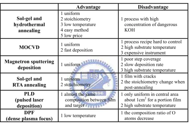
The advantages and drawbacks for the fabrication of the PZT thin film are showed in Table 2-1.
Table 2-1 Comparison of the various fabrication methods of PZT thin films
Advantage Disadvantage Sol-gel and hydrothermal annealing 1 uniform 2 stoichiometry 3 low temperature 4 easy method 5 low price
1 process with high
concentration of dangerous KOH
MOCVD 1 uniform 2 fast deposition
1 process recipe hard to control 2 high substrate temperature 3 expensive instrument Magnetron sputtering
deposition 1 uniform
1 poor step coverage 2 slow deposition rate 3 high substrate temperature Sol-gel and
RTA annealing
1 uniform 2 stoichiometry
1 film with cracks
2 the stoichiometry change when post-annealing
PLD (pulsed laser
deposition)
1 almost the same
composition between film and target
1 only uniform in central area about 1cm2 for a portion film
2 high substrate temperature DPF
(dense plasma focus) 1 low temperature
1 the composition ratio of O atoms decrease
2.3 Microwave System[30-32]
Microwaves are well-known as the rapid heating instruments. They have been used in the chemical synthesis to achieve and sustain high degree of temperatures within a very short time. However, chemists soon discover the additional advantages of tremendous rate enhancements and higher product yields. These rate enhancements have been found to increase the rate of reaction, even when run at the same temperature as a conventional reaction.
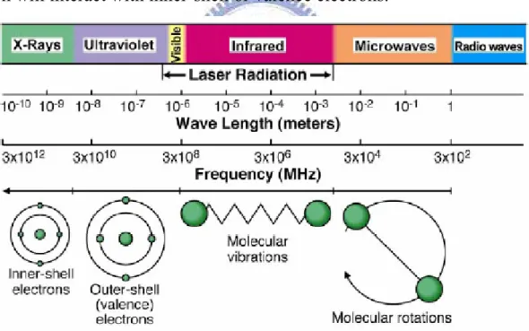
In the electromagnetic spectrum (~300Hz -300GHz), the microwave irradiation is a form of energy that falls in the low EM spectra in Fig. 2-1. This type of energy will only affect molecular rotations, unlike other forms of energy that you may be familiar with – IR, which will induce molecular vibrations; UV, which will interact with outer-shell electrons; and x-rays, which will interact with inner-shell or valence electrons.
The temperature of materials will rise up as the molecular rotation after irradiated by microwave. The rising rate of the temperature is relation to the dissipation factor of the materials, tangent δ, and defined as eq. (3)
(3)
where ε” is dielectric loss factor, ε’ is dielectric constant. From eq. (3), it can be seen that the dissipation factor (tangent δ) is proportional to the dielectric loss factor (ε”). So, the dielectric loss factor can be defined the ability of materials to absorb a specific frequency of the microwave under a specific temperature, and can also defined as the dissipation ratio of the microwave when penetrating materials. Table 2-2 shows the dissipation factor for several materials.
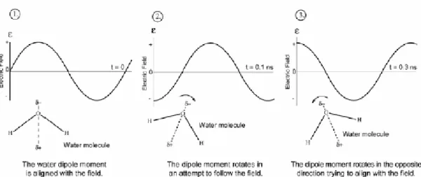
The microwave absorption for liquid phase can divide into two ways: dipole rotation and ionic conductance. Dipole rotation is an interaction in which polar molecules try to align themselves with the rapidly changing electric field of the microwave. The rotational motion of the molecule as it tries to orient itself with the field results in a transfer of energy, as depicted in Fig. 2-2. There are a number of factors that will ultimately determine the dipole rotation of coupling efficiency; however, any polar species (solvent and/or substrate) present will encounter this mechanism of energy transfer. The second way to transfer energy is ionic conduction, which occurs if there are free ions or ionic species present in the substance being heated. The electric field generates ionic motion as the molecules try to orient themselves to the rapidly changing field. This observation is similar with the dipole rotation and is shown in Fig. 2-3.
Table 2-2 The dissipation factor for several materials.
Materials Temperature(◦C) Tangent [δa×(10)b]
water 25 1570.0 fused quartz 25 0.6 ceramic F-66 25 5.5 porcelain No. 4462 25 11.0 phosphate glass 25 46.0 borosilicate glass 25 10.6
corning glass No. 0080 25 125.0
plexigalss 25 57.0 nylon66 25 128.0 polyvinyl chloride 25 55.0 polyethylene 25 3.1 polystyrene 25 3.3 teflon PFA 25 1.5
adissipation factor ( represented in tangent δ) ε”: dielectric loss factor
ε’ : dielectric constant
bthe frequency of microwave is 300Hz
Fig. 2-2 Three steps for dipole rotation.
Traditionally, the conductive heating is that the plate must heat the surface of the container before the heat can be transferred to the liquid. Then through the heat conduction of liquid provides the desired temperature. Because the center of the liquid is much cooler than the liquid near the glass, thermal currents are generated, which aids to the mixing of the liquid. This method of conventional heating requires couples of time. Fig. 2-4 shows the schematic diagram of the conductive heating.
Fig. 2-4 Schematic diagram of the conductive heating.
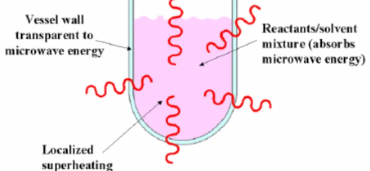
A microwave, however, activates the molecules directly, transferring energy to the reacting molecules themselves see in Fig. 2-5. All portions of the liquid phase in the vessel are simultaneously heating. This heating mechanism based on dipole rotation and ionic conductance is a very efficient way to heating in a short period. As mentioned previously, energy is added to the solution every nanosecond, causing a non-equilibrium condition where the molecules are constantly activated by the microwave energy.
2-4 The PZT Resonant Piezo-Layer Sensor[33]
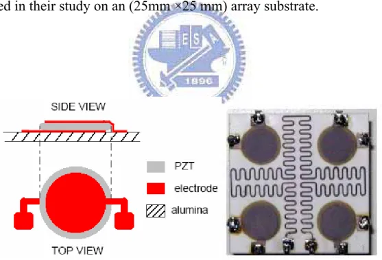
Recently, bulk acoustic-wave resonant piezo-layer (RPL) sensors made by lead zirconate titanate (PZT) thick films of screen-printed on alumina substrate have been proposed as gravimetric sensors for chemical detection in air matrix. Comparative experiments on cavitand-coated RPLs and QCMs are here firstly reported on the response to organic analytes of environmental interest. As shown in Fig. 2-6, the structure of a RPL sensor is fabricated by the superposition of non-piezoelectric substrate, specifically alumina, a bottom-electrode layer, a PZT layer poled along its thickness, and a top-electrode layer. RPLs offer similar mass sensitivity at parity of frequency with respect to QCMs and they can be easily manufactured as multisensor arrays on the same substrate. Four-sensor RPL arrays, as shown in Fig. 2-7, are reported in their study on an (25mm ×25 mm) array substrate.
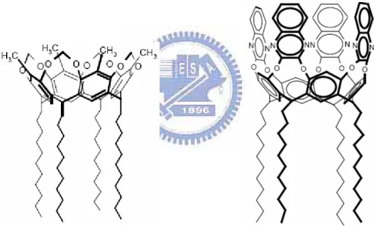
Cavitands used in this study exhibit supramolecular host properties which permit the incorporation of guests with a suitable polarity and shape. The Me-Cav illustrated in Fig. 2-8 has a more accessible and electron-rich cavity and can interact preferentially with analytes having ‘acidic’ methyl groups. The Qx-Cav shown in Fig. 2-9 presents a larger and deeper cavity formed by four quinoxalines. It is more adapted to interact with liphophilic organic guests, especially of aromatic origin. For RPLs, the sensors in the arrays have an electrode diameter of 5.5mm and a frequency of around 7 MHz. For both cavitands Me-Cav and Qx-Cav, 1 wt.% solutions were prepared in methylene dichloride.
Fig. 2-8 Host molecule of Me-Cav. Fig. 2-9 Host molecule of Qx-Cav.
Based on the reports, both RPL and QCM sensors immobilized with cavitand coatings exhibit the capability to detect organic vapors such as toluene and acetonitrile down to the concentration level of the order of 100 ppm.
2.5 Motivation
AT-cut thickness-shear mode quartz crystal microbalance (QCM) sensors are commonly used as gravimetric devices due to their good mass resolution at comparatively low operation frequency. From Sauerbrey equation, it can be seen obviously that sensitivity is improved when the surface area (A) is decreased and the resonance frequency of the unloaded resonator (fro) is
increased.
In this article, we proposed a piezoelectric material, PbZrxTi(1-x)O3 (PZT),
as a resonator to replace the quartz crystal. Although the dissipation factor (D) of PZT (10-3 –10-2) is more than that of quartz (10-6–10-4), the resonance frequency of PZT is higher and better. PZT also offers similar mass sensitivity at parity of frequency with respect to QCMs and it can be easily scale-down by photolithography as multisensor arrays and to improve the sensitivity.
As shown above, sol-gel and hydrothermal annealing under microwave system can provide a convenient method to deposited PZT thin films, and to reduce the post-annealing time to only several minutes. Besides, it can control the condition of both temperature and pressure during annealing. For example, the 13 vessels can be put simultaneously in the microwave system for processing at the same time. Especially, the microwave method utilizes the very low cost tool than other deposition tools and the cheap precursors.
From literatures[28,29], the reaction equation of hydrothermal annealing is in the following,
2Pb2+ + 2Zr4+ + 2Ti4+ + 6OH− → 2Pb(Zr, Ti)O3 + 3H2
but we find that it appears several obvious mistakes. The electrovalence is not equivalent and the production of hydrogen is not reasonable. We will pay more attention to deduce a reliable mechanism on hydrothermal annealing in this research.
Chapter 3 Experiments
3-1 Process of PZT Thin Films
The sol-gel solution of PZT obtained from Alfa Aesar (A Johnson Mattey Company) was spin-coated (WS-400 from Laurell Technology Corporation) on Pt/Cr/SiO2/Si wafer at 1000rpm for 10s and at 3000 rpm for
30s. The PZT films were subsequently prebaked at 150◦C for 10 min and at 350◦C for 30 min on a hot plate. The SiO2 layer, as a barrier layer, is deposited
by furnace to prevent the diffusion of Cr and Pt. Cr and Ti are both candidates for adhesion layer. However, the Ti is ruled out due to the possible etching away, while lithographic process of the device. Pt/Cr film was deposited by the dual e-gun evaporation system (Ulvac EBX-10C) and then annealed by RTA (HEATPLUSE 610) at 650◦C for 5 min.
The Hydrothermal treatment was carried out in a microwave reactor (CEM MARS-5) by immersing the substrate in 30 ml KOH + Pb(NO3)2 solution of
various concentrations. The concentration of KOH was varied from 0.5M, 1M to 2M, and Pb(NO3)2 was varied from 0.05M, 0.1M, 0.15M and 0.2M. The
substrate with PZT film was put in a Teflon beaker and covered by working solution in the microwave vessel. Prior to microwave heating, the vessel was purged under N2 atmosphere. The Teflon beaker was open with 3 holes to
afford the paths for ions and to prevent the reaction between the films and with the precipitation of the solution. It should be noted the PZT film would be oxidized to PbO2 and lost if the hydrothermal annealing was not under N2
atmosphere. The setup of the hydrothermal annealing is shown in Fig. 3-1. For each experiment, the microwave reactor was sealed and heated to the working temperature of 160◦C in 10min, and the system was maintained for 30min. The system was cooled after the hydrothermal treatment, and the samples were
rinsed in boiling deionized water. Finally the sample is and dried by a hot plate.
The film quality was analyzed by SEM (HITACHI S-4000), AFM (Veeco Dimension 5000 Scanning Probe Microscope), XRD (Shimadzu XD-5), and EDX (JEOL JEM 3000F).
Fig. 3-1 The setup of hydrothermal annealing in microwave system: (a) substrate, (b) solution, (c) Teflon beaker, (d) vessel (e) N2.
The Scanning Electron Microscope (SEM) is a microscope that uses electrons rather than light to form an image. The SEM uses electrons instead of light to form an image. A beam of electrons is produced at the top of the microscope by heating the metallic filament. The electron beam follows a vertical path through the column of the microscope. This design makes a better way through electromagnetic lenses which focus and direct the beam down towards the sample. Once it hits the sample, other electrons (backscattered or secondary) are ejected from the sample. Detectors collect the secondary or backscattered electrons, and convert them to a signal that is sent to a viewing screen similar to the one in an ordinary television, producing an image.
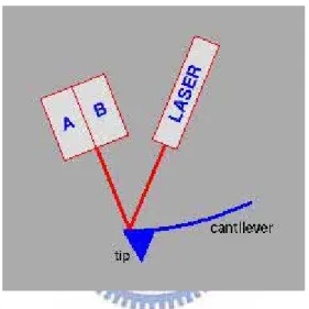
invented in 1986 by Binnig, Quate and Gerber. Like all other scanning probe microscopes, the AFM utilises a sharp probe moving over the surface of a sample in a raster scan. In the case of the AFM, the probe is a tip on the end of a cantilever which bends in response to the force between the tip and the sample. Figure 3-2 illustrates the working principle of AFM work. As if the cantilever flexes, the light from the laser is reflected onto the split photo-diode. By measuring the signal difference (A-B), various changes in the bending of the cantilever can be measured.
Fig. 3-2 The working principle of AFM.
There exist three main types of interaction, such as contact mode, tapping mode and non-contact mode. Contact mode is the most common method of operation for the AFM technique. As the name implies, the tip and the sample remain in close contact as the scanning proceeds. The so-called "contact" means the repulsive regime of the inter-molecular force curve. One of the drawbacks of remaining in contact with the sample is that there exist large lateral forces on the sample as the drip is "dragged" over the specimen.
Tapping mode is the next most popular mode used in AFM. When operated in air or other gases, the cantilever is oscillated at its resonant frequency (often hundreds of kilohertz) and positioned above the surface.
Therefore, it only taps the surface for a very small fraction of its oscillation period. When the imaging of contact mode is restricted by the unstable or soft samples, tapping mode may be a second choice than contact mode for imaging.
Non-contact operation is another method which may be employed when imaging by AFM. The cantilever must be oscillated above the surface of the sample at such a distance that we are no longer in the repulsive regime of the inter-molecular force curve. This is a very difficult mode to operate in ambient conditions with the AFM.
X-ray Powder Diffraction (XRD) is an efficient analytical technique used to identify and characterize unknown crystalline materials. Monochromatic x-rays are used to determine the interplanar spacings of the unknown materials. Samples are analyzed as powders with grains in random orientations to insure that all crystallographic directions are "sampled" by the beam. When the Bragg conditions for constructive interference are obtained, a "reflection" is produced, and the relative peak height is generally proportional to the number of grains in a preferred orientation. The x-ray spectra generated by this technique, thus, provide a structural fingerprint of the unknown. Mixtures of crystalline materials can also be analyzed and relative peak heights of multiple materials may be used to obtain semi-quantitative estimates of abundances. A glancing x-ray beam may also be used to obtain structural information of thin films on surfaces. In addition, changes in peak position that represent either compositional variation (solid solution) or structure-state information (e.g. order-disorder transitions, exsolution, etc.) are readily detectable. Peak positions are reproducible to 0.02 degrees of glancing angle.
SEM or TEM and is an efficient surface science technique. An electron beam strikes the surface of a conducting sample. The energy of the beam is typically in the range 10-20keV. This causes X-rays to be emitted from the point where the material is irradiated by the primary electron beam. The energy of the X-rays emitted depends on the material for examination. The X-rays are generated in a region about 2µm in depth, and thus EDX is not an actual surface science technique. The detector used in EDX is the Lithium drifted Silicon detector. This detector must be operated at liquid nitrogen temperatures. When an X-ray photon strikes the detector, it will generate a photoelectron within the body of the Si. As this photoelectron travels through the Si, it generates electron-hole pairs. The electrons and holes are attracted to opposite ends of the detector with the aid of a strong electric field. The size of the current pulse thus generated depends on the number of electron-hole pairs created, which in turn depends on the energy of the incoming X-ray. Thus, an X-ray spectrum can be used to acquire the giving information on the elemental composition of the interest material under examination.
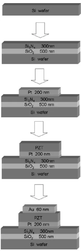
3-2 Process of PZT Sensors
Figure 3-3 shows the process of a PZT sensor. The SiO2 500nm and Si3N4
300nm were deposited on Si wafer by a furnace. The purpose of Si3N4 layer is
to prevent the possibility of device damage by KOH while the hydrothermal annealing. The adhesion layer (Cr) and the bottom electrode (Pt) were sequentially deposited on the lithographic pattern of SiO2/Si3N4/Si wafer. Then,
the resist is removed by the specific solvents. The sample is annealed by RTA (HEATPLUSE 610) at 650◦C for 5min. The sol-gel solution of PZT obtained from Alfa Aesar (A Johnson Mattey Company) was coated on the Pt/Cr/Si3N4/SiO2/Si wafer by spin-coater (WS-400 from Laurell Technology
Corporation) at 1000rpm for 10s and at 3000rpm for 30s. This pattern is designed by the exposure on photoresist, and etched away by HCl. The PZT films then were treated by the specific hydrothermal annealing in the microwave system. Finally, we also use the lift-off process to define the the top electrode (Au) and adhesion layer (Cr) prior to deposite the electrode by thermal coater, the photoresist pattern is defined. The developed PZT sensors were used to detect the organic vapor, including of the alcohol, toluene and acetone. The gas molecules were adsorbed on the sensors by only the physical adsorption. The frequency shifts were detect by the frequency counter (Agilent 53132A) and recorded by computer in real-time.
Chapter 4 Results and discussion
4-1 The Mechanism of Hydrothermal Annealing
There is a white precipitation while Pb(NO3)2 is added into the KOH
solution. We suppose the formation of Pb(OH)2 due to the similar report of
using Pb(NO3)2 in the literature[25,26]. The PZT thin film is composed of PbO,
ZrO2 and TiO2. The hydrothermal annealing is the best way to precipitate the
PbO on the porous ZrO2+TiO2 network from the solution. The possible
chemical reaction is shown in the following, Pb(OH)2 → PbO + H2O
As shown in Fig. 4-1, the portion of PZT film is lost due to the contact with the precipitation of the solution. We design a special teflon beaker with 3 holes for avoiding the damage of PZT film. The hole only allows the reactive ions to pass in and out. This design can avoid the PZT film reacting with the precipitation and get lost. The possible chemical reaction is shown in the following,
Pb(OH)2 → Pb2+ + 2OH
-Pb2+ + 2OH- → PbO + H2O
Besides, PbO is an active compound. The reaction must be controlled in N2
atmosphere, otherwise the film would be lost as if PbO oxidizing to PbO2.
Fig. 4-1 The morphology of PZT film after hydrothermal annealing. Δ
4-2 Characterization of PZT Thin Films 4-2.1 SEM Analysis
Figure 4-2 shows the SEM micrographs for PZT thin films with different recipes of the hydrothermal annealing. Figure 4-2 (a) is the morphology of the PZT film without annealing, and some significant cracks is appeared ton the surface. These cracks are originated from the vaporization of the organic precursor during the sol-gel synthesis. From the above mechanism of hydrothermal annealing, the PZT films will become rough either at low concentration of KOH or at insufficient amount of Pb(NO3)2. Since the leakage
of reactants would induce the lack of Pb2+ or OH- ions, it would affect the nucleation and growth of the film. The PZT film will be dissolved by KOH and be removed when the concentration of solution is 0.5M KOH + 0.05M Pb(NO3)2. Figure 4-2 (b) to (d) shows the PZT films after annealing under
0.5M KOH, and Pb(NO3)2 of 0.1M, 0.15M and 0.2M. The morphology are
very rough for the PZT films using 0.5M KOH. There are only few dispersive regions with PZT nucleation and growth. When the PZT films are treated in 1M KOH + 0.05M Pb(NO3)2 and 1M KOH + 0.1M Pb(NO3)2 solution, the
surfacecoverage of the film is found due to the higher extent of nucleation and growth. The film is still rough shown in Fig. 4-2 (e) and (f). In Fig. 4-2 (g) and (h), although there are also several cracks, the roughness of the film seems to be better at the concentration of 1M KOH + 0.15M Pb(NO3)2 or 1M KOH +
0.2M Pb(NO3)2. As increasing the solution concentration to 2M KOH + 0.05M
Pb(NO3)2 and 2M KOH + 0.1M Pb(NO3)2, the surface film are still not suitable
coverage with nucleation and growth, illustrated in Fig. 4-2 (i) and (j). When the solution are optimized to 2M KOH + 0.15M Pb(NO3)2 and 2M KOH +
0.2M Pb(NO3)2, the quality of the films seems to become better, and the
saturation of Pb(NO3)2 is near 0.15M. This observation are just similar with
Fig. 4-2 The SEM micrographs of PZT thin film with hydrothermal annealing: (a) before annealing
(c) KOH=0.5M, Pb(NO3)2=0.15M
(e) KOH=1M, Pb(NO3)2=0.05M
(g) KOH=1M, Pb(NO3)2=0.15M
(i) KOH=2M, Pb(NO3)2=0.05M
(k) KOH=2M, Pb(NO3)2=0.15M
4-2.2 AFM Analysis
Figure 4-3 shows the AFM micrographs of the surface of PZT thin films. The morphology is also helpful to observe the nucleation and growth of the films from roughness. Figure 4-3 (a) is the PZT film without annealing which can be observed that the film is amorphous and with several cracks on it. When the solution concentration are 0.5M KOH + Pb(NO3)2 (0.1M, 0.15M
and 0.2M), no obvious nucleation and growth on the films are observed. But the films are rougher than that without annealing, as depicted in Fig. 4-3 (b) to (d). From Fig. 4-3 (e) to (g) at 1M KOH + Pb(NO3)2 (0.1M, 0.15M and 0.2M)
solution, it can be apparently seen that the PZT nucleation can have small grain sizes. However, the films are still rough because of not growth yet. Interestingly, as shown in Fig. 4-3 (h) and (i), when the concentration is 2M KOH + 0.15M Pb(NO3)2 or 2M KOH + 0.2M Pb(NO3)2, the crystallization are
obviously and the surface roughness can be avoided than that without annealing. Besides, when the concentration is 0.05M Pb(NO3)2 and 2M KOH
+ 0.1M Pb(NO3)2, the films is seriously crack, even can be seen by naked eyes.
Fig. 4-3 The AFM micrographs of PZT thin film with hydrothermal annealing: (a) before annealing
(b) KOH=0.5M, Pb(NO3)2=0.1M
(d) KOH=0.5M, Pb(NO3)2=0.2M
(e) KOH=1M, Pb(NO3)2=0.1M
(g) KOH=1M, Pb(NO3)2=0.2M
(h) KOH=2M, Pb(NO3)2=0.15M
4-2.3 XRD Analysis
XRD patterns of the samples treated by hydrothermal annealing are shown in Fig. 4-3. These patterns are all analyzed by JCPDS (Joint of committee on powder diffraction standards) data base. Only the amorphous structure is observed in the as-deposited PZT films, prior to the hydrothermal treatment. When the reaction solutions are operated in 0.5M KOH, there are still amorphous structures, as shown in Fig. 4-3 (a). Whereas the weak perovskite phase was observed in the films after typical run of the hydrothermal treatments under 1M KOH + 0.15M Pb(NO3)2 and 1M KOH +
0.2M Pb(NO3)2 solutions, of which shown under Fig. 4-3 (b). However the
perovskite phase with a preferred (111) and (003) orientations were clearly observed in these as-deposited PZT films after a typical run of the hydrothermal treatment in 2M KOH + 0.15M Pb(NO3)2 and 2M KOH + 0.2M
Pb(NO3)2 solutions, as shown in Fig. 4-3 (c). From the SEM and AFM
micrographs, it can be observed that there are crystallization and growth for PZT films. However, there are not strong peaks in XRD patterns. We suppose that the films are with random orientation.[31] Except for the peak of PbO2 in
Fig. 4-3 (c) at concentration of 2M KOH + 0.05M Pb(NO3)2 and 2M KOH +
0.1M Pb(NO3)2 solutions, we think the films would be oxidized to produce
(a)
2 0 2 5 3 0 3 5 4 0 4 5 5 0 5 5 6 0 2 θ(d eg ree) In te n si ty( a .u. ) P t ( 111 ) (v) KOH=0.5M, Pb(NO3)2=0.2M PbO ( 003 )(iv) KOH=0.5M, Pb(NO3)2=0.15M
(iii) KOH=0.5M, Pb(NO3)2=0.1M
(ii) KOH=0.5M, Pb(NO3)2=0.05M
(i) before annealing
Fig. 4-4 The XRD patterns of PZT thin films with hydrothermal annealing: (a) KOH=0.5M
(b)
20 25 30 35 40 45 50 55 60 2θ(degree) In ten sity (a .u .) P t ( 111 ) (v) KOH=1M, Pb(NO3)2=0.2M(iv) KOH=1M, Pb(NO3)2=0.15M
PbO
2
(
200
) (iii) KOH=1M, Pb(NO3)2=0.1M
(ii) KOH=1M, Pb(NO3)2=0.05M
(i) before annealing
(c) 20 25 30 35 40 45 50 55 60 2θ(degree) In ten sity (a .u .) PbO (1 11 ) P t ( 111 ) (v) KOH=2M, Pb(NO3)2=0.2M PbO ( 003 )
(iv) KOH=2M, Pb(NO3)2=0.15M
PbO 2 ( 200 ) (iii) KOH=2M, Pb(NO3)2=0.1M
(ii) KOH=2M, Pb(NO3)2=0.05M
PbO
2
(
200
)
(i) before annealing
PbO (1
11
)
4-2.4 EDS Analysis
From the mechanism of the hydrothermal annealing, the treatment is aimed to control the dissolution-reaction-crystallization. Since the piezoelectric property of PZT is related to the morphology phase boundary (MPB) as the competition, we characterize the PZT films by EDS to see whether the competition is changed during the hydrothermal annealing. Table 4-1 shows the analysis of PZT films with the hydrothermal treatments by EDS. When the working solution is adjusted to 2M KOH + 0.15M Pb(NO3)2 and 2M
KOH + 0.2M Pb(NO3)2 , the competition of the films are also similar to that
without annealing. However, the ratios of the elements analyzed by EDS are different with the source, Pb(Zr0.52Ti0.48)O3. The films are only about 750nm
which could be transmitted by the electron of EDS and make the analysis more difficult. But, it can still provide the evidence that the competition of the films are almost the same after hydrothermal annealing with 2M KOH + 0.15M Pb(NO3)2 and 2M KOH + 0.2M Pb(NO3)2 solutions.
Table 4-1 The analysis of PZT thin films by EDS with hydrothermal annealing.
2M KOH before annealing 0.05M Pb(NO3)2 0.1M Pb(NO3)2 0.15M Pb(NO3)2 0.2M Pb(NO3)2 Pb 18.37% 41.95% 59.62% 16.83% 17.78% Zr 77.35% 56.15% 37.56% 73.37% 77.35% Ti 4.28% 1.90%* 2.82% 9.80% 4.87% 1M KOH befroe annealing 0.05M Pb(NO3)2 0.1M Pb(NO3)2 0.15M Pb(NO3)2 0.2M Pb(NO3)2 Pb 18.37% 71.52% 24.68% 24.34% 23.44% Zr 77.35% 21.70% 70.38% 72.19% 70.69% Ti 4.28% 6.27% 4.94% 3.46% 5.88% 0.5M KOH before annealing 0.05M Pb(NO3)2 0.1M Pb(NO3)2 0.15M Pb(NO3)2 0.2M Pb(NO3)2 Pb 18.37% 57.14% 25.55% 24.41% 22.95% Zr 77.35% 37.86% 70.36% 68.04% 71.68% Ti 4.28% 4.99% 3.53% 7.56% 5.37%
4-3 Application of PZT Sensors for Chemical Analysis
In previous sections, we have successfully identified the film quality by SEM, AFM, XRD and EDS. The most appropriate hydrothermal annealing is chosen by 2M KOH + 0.2M Pb(NO3)2 solution. The PZT thin film is applied to the
chemical sensor. Figure 4-5 shows the top view of the PZT sensor with 4 × 4 array. Each array is about 3cm × 1cm and with 16 PZT sensors with radius of 600μm. The structure of a PZT sensor is just similar to a common QCM which is also a piezoelectric material between two electrodes. The bottom electrode is Pt in order to get crystallized PZT thin films, and the top electrode is Au to prepare for the advanced application in biosensor and bonding with DNA or proteins.
4-2.1 The Qualitative Analysis by PZT Sensors
Typical experiments consisted of the following sequences. The sensors were put in a closed system, and the resonant frequency of the sensors reached the steady state. The frequency output of all the sensors was recorded every second. The PZT sensors were first used to characterize the spraying solutions such as alcohol, acetone and toluene. The qualitative analysis is established in order to see whether the sensor could work as using PZT instead of quartz crystal. Figure 4-6 shows the frequency shifts of alcohol, acetone and toluene. Although the noise signal is still significant, it can apparently observe the frequency shifts after the solution sprayed on the sensors. The frequency shifts of spray alcohol, acetone and toluene are 27kHz, 8.6kHz and 4.7kHz. However, the differences of the frequency shifts may come from the different quantity on the sensor. It provides a preliminary success of the PZT sensor.
(b) The spray of acetone.
4-2.2 The Quantitative Analysis by PZT sensors
Although the experiments reported here are following with the quantitative analysis of PZT sensors with vapors of alcohol and toluene. The sensors and a beaker were both put in a closed system until the resonant frequency of the sensors reached the steady state. Then, we injected the solution into the beaker. The solution would be vaporized and saturated with vapor in the closed system. The molecules of the vapor would diffuse and be adsorbed on the Au electrode. Since it is only a physical adsorption of the molecules, the PZT sensor can be recycled without any damage. The saturated vapor pressures are different under various temperatures. As we know the theoretical values of saturated vapor pressures, we can multiply the area of the electrode and achieve the quantitative analysis. The frequency shifts of alcohol vapor in Fig.4-6 are 8.3kHz, 23.7kHz, 42kHz and 66.7kHz in 30℃, 40℃, 50℃ and 60℃, respectively. The noise is not ignored since affected by the fan oven, but the frequency shifts also can be seen obviously. The frequency shifts of toluene vapor are in Fig. 4-7 6.6kHz, 11.8kHz, 15.5kHz and 18.9kHz at 30℃, 40℃, 50℃ and 60℃, respectively.
Fig. 4-7 The shift frequency of a PZT sensor: (a) by vapor of alcohol at 30℃.
(c) by vapor of alcohol at 50℃
Fig. 4-8 The shifted frequency of a PZT sensor: (a) by vapor of toluene at 30℃.
(c) by vapor of toluene at 50℃
However, there would be no frequency shift without any vapor pressure. Hence, we plotted the frequency shifts and saturated vapor pressures of alcohol and toluene with respect to temperatures as shown in Fig. 4-8, of which combined the experimental and theoretical values. The black points are the frequency shifts of the solutions from the experimental values, while the white points are the saturated vapor pressures of the solutions from the theoretical values. From Fig. 4-8 (a), the experimental and theoretical values almost fit in the same trend. Hence, the sensitivity of the PZT sensors is quite reliable for sensing the vapor of alcohol. Interestingly, the experimental and theoretical values do not match together while sensing the vapor of toluene, as depicted in Fig. 4-8 (b). The errors may be attributed to the noise produced by the sensing environment. Because toluene is a kind of solution with low vapor pressure, we supposed that the noise would be bigger relative to the frequency shifts. But, it is still behaved in the same tendencies for the two curves. Therefore, the sensitivity of the PZT sensor is also reliable when sensing toluene. From the results of quantitative analysis, we can also calculate the theoretical value of the sensing limit to be about 1ppm without coating anything on the sensor.
Fig. 4-9 The shift frequency of a PZT sensor with the vapor pressure: (a) alcohol, (b) toluene.
Chapter 5 Conclusions
The combination of the sol-gel method and the hydrothermal process in microwave system can be successfully used to prepare polycrystalline PZT thin films at the temperature of 160◦C in 30ml 2M KOH + 0.2M Pb(NO3)2 solution. The hydrothermal annealing in microwave system can
shorten the reaction time and improve the efficiency. Because the reaction in each vessel uses only 30ml solution, the annealing method can also be attributed to fit the requirement of green energy. The hydrothermal treatment mechanism, for the first time, is proposed to follow dissolution-reaction-crystallization below.
Pb(OH)2 → PbO + H2O
Pb(OH)2 → Pb2+ + 2OH -Δ
Pb2+ + 2OH- → PbO + H2O
The PZT sensors, without coating anything, showed the ability to detect organic vapors like alcohol and toluene. The curve of the frequency shifts and the saturated pressure almost match together for alcohol. The toluene gas can also be detected in the similar way. The sensing performance of the PZT sensor is quite reliable. The resonant frequency of the sensor is about 30MHz and the sensing limit is estimated to be about 1ppm.
Δ
Since the PZT sensors are sensitive and reliable in sensing volatile vapor, we plan to improve the efficiency by the array design. The developed PZT sensor can be extended to detect other biomolecules like DNA or proteins in the future.
Reference
[1] J. F. Tressler, S. Alkoy and R. E. Newnham, “Piezoelectric Sensors and Sensor Materials”, Journal of Electroceramics, 2, 257-272 (1998)
[2] C.K. O’Sullivan and G.G. Guilbault, “Commercial quartz crystal microbalances – theory and applications”, Biosensors & Bioelectronics, 14, 663-670, (1999)
[3] http://www.txc.com.tw/in04/in4_01.html
[4] M. Rodahl, F. Höök, A. Krozer, P. Brzezinski and B.Kasemo, “Quartz crystal
microbalance setup for frequency and Q-factor measurements in gaseous and liquid environments”, Review of Scientific Instruments, 66, 3924-3930, (1995)
[5] M. Rodahl and B. Kasemo, “A simple setup to simultaneously measure the resonant frequency and the absolute dissipation factor of a quartz crystal microbalance”, Review of Scientific Instruments, 67, 3238-3241, (1996)
[6] B. D. Vogt, E. K. Lin, W. L. Wu and C. C. White, “Effect of Film Thickness on the Validity of the Sauerbrey Equation for Hydrated Polyelectrolyte Films”, Journal of Physical Chemistry B, 108, 12685-12690, (2004)
[7] T. D. Hadnagy, “Materials and production characterization requirements for the
production of FRAM(R) memory products”, Integrated Ferroelectrics, 18, 1-17, (1997) [8] B. Noheda, J. A. Gonzalo, L. E. Cross, R. Guo, S. E. Park, D. E. Cox and G. Shirane,
“Tetragonal-to-monoclinic phase transition in a ferroelectric perovskite: The structure of PbZr0.52Ti0.48O3”, Physical Review B, 61, 8687-8689, (2000)
[9] P. Birounvand, M. H. Berntsen, J. Penttilä, S. Shokatloo and M. Wahlqvist, “Biosensors based on piezoelectric materials: Indoor air monitoring and detection of bacterial spores”, Royal Institute of Technology, (October 2005)
[10] R. E. Alonso, A. L. García, A. Ayala and P. de la Presa, “Temperature dependence of the nuclear quadrupole interaction at Zr–Ti sites in PbZrxTi.1−xO3 in the Zr-rich
(1998)
[11] P. Muralt, “Ferroelectric thin films for micro-sensors and actuators: a review”, Journal of Micromechanics and Microengineering, 10, 136-146, (2000)
[12] C. M. Foster, G. R. Bai, R. Csencsits, J. Vetrone, R. Jammy, L. A. Wills, E. Carr and J. Amano, “Single-crystal Pb(ZrxTi1-x)O3 thin films prepared by metal-organic chemical
vapor deposition: Systematic compositional variation of electronic and optical properties”, Journal of Applied Physics, 81, 2349-2357, (1997)
[13] Y. Sakashita, H. Sagawa, K. Tominaga and M. Okada, “Dependence of
electrical-properties on film thickness in Pb(ZrXTi1-X)O3 thin-films produced by
metalorganic chemical-vapor-deposition”, Journal of Applied Physics, 73, 7857-7863, (1993)
[14] K. Nagashima and H. Funakubo, “Composition control of Pb(ZrxTi1-x)O3 thin films
prepared by metalorganic chemical vapor deposition”, Japanese Journal of Applied Physics Part 1, 39, 212-216, (2000)
[15] B. S. Kwak, E. P. Boyd and A. Erbil “MOCVD of PbTiO3 thin films”, Applied Physics
Letters, 53, 1702–1704, (1988)
[16] I. Kanno, S. Fujii, T. Kamada and R. Takayama, “Piezoelectric properties of c-axis oriented Pb(Zr,Ti)O3 thin films”, Applied Physics Letters, 70, 1378-1380, (1997)
[17] I. Taguchi, A. Pignolet, L. Wang, M. Proctor, F. Lavy and P. E. Shmid, “Raman-scattering from PbTiO3 thin-films prepared on silicon substrates by
radio-frequency sputtering and thermal-treatment”, Journal of Applied Physics, 73, 394-399, (1993)
[18] T. Hase, T. Sakuma, Y. Miyasaka, K. Hirata and N. Hosokawa, “Preparation of Pb(Zr, Ti)O3 thin-films by multitarget sputtering”, Japanese Journal of Applied Physics Part 1,
32, 4061-4064, (1993)
sputtering and characterization of ferroelectric PZT films”, Journal of Applied Physics,
54, 6601–6609, (1983)
[20] K. Sreenivas, M. Sayer and P. Grarett et al, “Properties of dc magnetron-sputtered PZT thin films”, Thin Solid Films, 172, 251–267, (1989)
[21] T. Nakamura, Y. Nakao, A. Kamisawa and H. Takasu, “Preparation of Pb(Zr,Ti)O3
thin-films on Ir and IrO2 electrodes”, Japanese Journal of Applied Physics Part 1, 33,
5207-5210, (1994)
[22] T. Astuki, N. Soyama, G. Sasaki, T. Yonezawa, K. Ogi, K. Sameshima, K. Hoshiba, Y. Nakao and A. Kamisawa, “Surface-morphology of lead-based thin-films and their properties”, Japanese Journal of Applied Physics Part 1, 33, 5196-5200, (1994)
[23] C. J. Kim, D. S. Yoon, J. S. Lee, C. G. Choi and K. S. Nol, “Effects of substracte effect of substracte and bottom electrodes on the phase-formation of lead-zirconate-titanate thin films prepared by the sol-gel method”, Japanese Journal of Applied Physics Part 1,
33, 2675-2678, (1994)
[24] Y. C. Zhou, Z. Y. Yang and X. J. Zheng, “Residual stress in PZT thin films prepared by pulsed laser deposition”, Surface & coatings technology, 162, 202-211, (2003) [25] M. C. Kim, J. W. Choi, S. J. Yoon, K. H. Yoon and H. J. Kim, “Thickness dependence
of Pb(Zr0.52Ti0.48)O3 films prepared by pulsed laser deposition”, Japanese Journal of
Applied Physics Part 1, 41, 3817-3821, (2002)
[26] Y. Masuda, T. Nozaka , “The influence of various upper electrodes on fatigue
properties of perovskite Pb(Zr,Ti)O3 thin films”, Japanese Journal of Applied Physics
Part 1, 42, 5941-5946, (2003)
[27] R. Gupta, M. P. Srivastava, V. R. Balakrishnan, R. Kodama and M. C. Peterson, “Deposition of nanosized grains of ferroelectric lead zirconate titanate on thin films using dense plasma focus”, Journal of physics D, 37, 1091-1094, (2004)
at low-temperature of less than 400◦C by hydrothermal treatment following sol-gel deposition”, Japanese Journal of Applied Physics Part 1, 40, 5539-5542, (2001) [29] Z. WEI, K. Yamashita and M. Okuyama, “low temperature preparation of sol-gel PZT
thin film annealed at 160°C by hydrothermal method”, Applications of ferroelectrics, 2, 921-924, ISAF 2000. Proceedings of the 2000 12th IEEE International Symposium, (2000)
[30] E. K. Barnhardt and B. L. Hayes, “Performing microwave-assisted reactions at low temperatures preliminary results”, the 226th ACS National Meeting New York, NY, (September 9, 2003)
[31] E. Nest, M. Collins, Introduction to microwave sample prearation theory and pratice, (1998)
[32] H. M. Kingston and S. J. Haswell, Microwave-Enhance Chemical,American Chemical Society, Washington DC, (1997)
[33] M. Ferrari, V. Ferrari, D. Marioli, A.Taroni, M. Suman and E. Dalcanale, “Cavitand-coated PZT resonant piezo-layer sensors: properties, structure, and comparison with QCM sensors at different temperatures under exposure to organic vapors”, Sensors and Actuators B, 103, pp. 240-246, (2004)
[34] Q. M. Wang, Y. Ding, Q. Chen and M. Zhao, “Crystalline orientation dependence of nanomechanical properties of Pb(Zr0.52Ti0.48)O3 thin films”, Applied Physics Letters,