Analysis and modelling
of
initial delay time and its
impact on propagation delay of CMOS logic gates
Y.-H. Yang c.-Y. wu
indexing term : Metal-Oxide-semiconductor structures, Modelling
Abstract: The initial delay times due to the capac- itive feedthrough effects in CMOS inverters are characterised and investigated. Based on the MOSFET large-signal model, the initial delay is modelled for a chain of CMOS inverters under step and ramp inputs. Optimal design that results in the minimum initial delay is obtained. Correla- tion between the initial delay and the propagation delay is constructed in the case of characteristic waveforms. The initial delays are found to deter- mine the propagation delay. Applying the model to evaluate the speed performance of a scaled- down CMOS, the delay improvements for various scaling laws are compared. It is found that the most effective law in reducing the initial delay for internal circuits is the constant voltage law, whereas that for the input stage is the constant electric field law. Comparisons to SPICE simula- tion results are also given and good agreement is achieved. List of symbols A,(,, CJ CJsw C,,,, Ces(d)o
C L =loading capacitance of chain of CMOS
Con,,) = oxide capacitance of n-(p-) channel MOSFET D E L T A = parameter of narrow width effect for thresh- L,,,, = effective channel length of n-(p-) channel
L,,, = effective channel length of MOSFET
MJ,(,, = bulk-junction bottom grading coefficient of M,,,,,,, = bulk-junction sidewall grading coefficient of Nsvb = substrate doping concentration
P B = bulk-junction potential P,(,,
4
= area of source (drain) region
= zero-bias bulk-junction bottom capacitance = zero-bias bulk-junction sidewall capacitance = bulk-drain (source) junction capacitance = gate-source (drain) overlap capacitance
per unit area per unit length
inverters in each stage
old voltage MOSFET
n-(p-) channel MOSFET n-(p-) channel MOSFET
= perimeter of source (drain) region = magnitude of electronic charge
~~ Paper 67686 (ElO), first received 26th September 1988 and in revised form 30th January 1989
The authors are with the Department of Electronics Engineering and Institute of Electronics, National Chiao Tung University, Hsin Chu, Taiwan, Republic of China
1 E E P R O C E E D I N G S , Vol. 136, Pt. G, No. 5, OCTOBER 1989
T,, = gate oxide thickness
Vmox = maximum drift velocity of carrier VTo = threshold voltage under zero bias
VTn(,) = threshold voltage of n-(p-) channel MOSFET
Vbs
= voltage drop between bulk and source regionsI:
= thermal voltageWnCp, =effective channel width of n-(p-) channel We, = dimension of source/drain regions in channel X , = metallurgical junction depth
E,(,, = geometrical factor of source (drain) junction with short-channel effect
= transconductance parameter of n-(p-) channel MOSFET
/In,,) = channel-length modulation parameter of n-(p-) channel MOSFET
= bulk threshold parameter of long channel n-(p-) channel MOSFET
MOSFET length direction
eSilox, = permittivity of silicon (silicon dioxide)
p, = surface mobility
p,,,, = mobility of n-(p-) channel MOSFET
pL,,it = critical field coefficient for mobility degradation p e x p = critical field exponent for mobility degradation pLtro = transverse field coefficient
4F
= Fermi potential1 Introduction
The advantages of low-power consumption and high- noise immunity make CMOS the main technology in
VLSI and ULSI [
11.
Ideally, the signal of a CMOS logic gate is rail-to-rail between the power supply (VDD) and ground ( G N D ) . However, transient simulations show that the actual transient voltage level at the output node of a CMOS logic gate is greater than VDD or smaller than G N D during certain periods. When this voltage over- shoot or undershoot occurs, a charging or discharging current, opposite in direction to the normal output device currents, is generated on the device capacitance and fed to the output node of the gate to increase the voltage above V,, or decrease it below GND. Owing to such a capacitive feedthrough effect, extra delay time, called the initial delay time, is needed to remove those excess feed- through charges at the output node and recover the signal to its normal level. It is found that this initial delay time usually dominates the total signal delay [2], espe- cially in the case that the input waveform has finite rise or fall time. The speed performance of a CMOS gate istherefore strongly affected by the initial delay times. However, it has not yet been well characterised in recent timing papers [2-71.
To obtain a better understanding of initial delays, and since the behaviour of other CMOS inverting logic gates can be understood from that of the basic inverter, initial delays of CMOS inverters are investigated and analysed in this paper. Taking the physical nature of transient waveforms into consideration, and using the analytical current equations [S-1 I] which consider the small- geometry effects, the initial delays of CMOS inverters under step and ramp input excitations are analytically modelled. Based on the developed analytical models, the dependence of initial delay on the input slope, device parameters and the loading capacitance is investigated. Optimal device dimension resulting in minimum initial delay can also be derived.
Comparisons between the model calculations and SPICE [SI simulations for wide ranges of device dimen- sions, input slope and loading capacitance are given for step and ramp inputs, respectively. Good agreement is obtained. The correlation between the initial delay and the propagation delay of C M O S inverters is observed in the characteristic waveform case 1123. The model devel- oped in Section 2 . 2 is modified to account for the depen-
dence of input slope on device parameters, in the characteristic waveform case, and is applied to investigate the initial delay or the propagation delay of CMOS inverters scaled down according to various scaling laws [13, 141. The experimental results of initial delay for various device dimensions and input ramp rates are also shown.
2 Models 2. I Step input
2.1.1 Initial fall delay: Consider a chain of p-well CMOS inverters as shown in Fig. 1. When a step input
VD D vOD VDD
P
P
- .
Fig. 1 Chain of identicul CMOS inuerters
voltage v4t) raises to Vo0 instantly, the output voltage F ( t ) first overshoots above V,, and then decreases back to V,, at t = t d / (the initial fall delay). The input-voltage waveform and part of the output waveform are shown in Fig. 2a by solid lines in an enlarged scale; the waveforms in the undershoot case are also shown.
T o determine the operating regions of MOSFETs, the drain-source saturation voltage
brat,
considering the velocity saturation effect, is calculated. The resultantbsor
curve for the NMOS M I , in the overshoot case is shown in Fig. 2a. It can be seen from Fig. 2a that M I , is oper- ating in the saturation region from t = 0 to t = t d / . During this period, however, the output node becomes the source node of the PMOS M , , because its voltage is greater than V,,. whereas the node connected to the power supply V', acts as the drain. This is opposite to the normal case and a positive substrate bias results, so that the magnitude of the PMOS threshold voltage is reduced [SI. M , , will be turned on in the saturation 246region for a sufficiently large voltage overshoot. It is found, however, that the time interval when MI, is
6 r (frnox*Vornux) VDD=5V
L
( t r n m k r n i n ) -1 I I I -0.2 0 0.2 0.4 0.6 0.8 time. ns a V,(t):Jm(t)
f I&) t Ip(t) - - b Fig. 2U Schematic diagram of Input and output voltage waveforms under step input h Large-signal equivalent circuil of CM OS mverter chain
turned on is rather short and the current generated by
M I , can be reasonably neglected, as compared with the
transient current of the bulk-source junction capacitance
C b , , . M I ? is therefore assumed to be off during the over-
shoot period. The DC current of the bulk-source junction can also be neglected, as compared with its capacitance transient current in this short period.
Since the voltage at the output node of the second stage remains unchanged during the overshoot period, the output node of the second stage can be effectively grounded. Thus, applying the MOSFET large-signal model t o the four devices in the first two stages [23, the overall equivalent circuit during the initial fall delay can be obtained as shown in Fig. 26. In Fig. 26, the current I , ( f ) and the DC current of the source-substrate junction of M , , are neglected, whereas I,(r) is the saturation current of M , , and can be written as [S, IO]
= f l A ( v g s n - - q n vdsotn/2)vdsan - 2?sm/3 [ ( 2 d ) F n
+
Vdsoin - vbsn)3'2 ~ ( 2 $ F n ~ v b s n ) 3 / 2 1 }x ( 1
+
2,Vdm)
(1)where the drain-source saturation voltage
bsotn
can be solved from [ 1 S ]Considering the velocity saturation effect, the channel- length modulation parameter 2, in eqn. 1 can be IEE PROCEEDINGS, Vol. 136. Pt G, N o 5 , O C T O B E R 19x9
The capacitances C , , C, and C, in Fig. 2h can be expressed as [S, 111
Ci = C p , + Cg,,p
+
2 C J 3c,
=cgdan
+
c,,,,
+
2c0,i3c,
=c,,,,
+
c,,,,
+
C,,,"+
Cgdan+
CO"+
CO,+
CL (4) ( 5 )(6) and the voltage-dependent p-n junction capacitances C,,, and C,,, can be written as [SI
C b d n ( C b s p ) = CJn(p) - b d m ( b s p ) / p B n < p ) ) M'"'n'
+
c J S W n ( p ) psn(p)(l - b n , b s p ) / p B n , p l ) -'M'SWn'u' (7)In eqns. &6, the loading capacitance C L and the gate- oxide capacitances CO, and CO, have larger effect on C, and C, than other capacitances.
To analytically solve the output voltage V,(t), neces- sary simplifications must be applied to linearise the current and capacitances. First, the channel-length modu- lation parameter I , and other V,,,- and V,,,-dependent parameters are all evaluated at V, = V , = VD,
.
This leads to the linear dependence of f , ( t ) onb,..
Secondly, the capacitances Cbdn and C,,, are assumed to be constant in solving L$(t). After the explicit expression of V,(t) is obtained, the voltage dependencies of C,,, and C,,, are incorporated into the expression of Vo(t) to form a non- linear equation. Iterations are then applied to get the final results.Based upon the above assumptions, V , ( t ) can be solved as
K(')
[(I+
+
c 3 f+
c b s p ) ) % D+
l/In]e-"' ~ (8)I E E P R O C E E D I N G S , Vol. 136, P i . C , N o . 5 , OCTOBER I989
K m a x = 'DD + ' 2 v D D / ( c 2
+
'3+
+
' h s p ) (lo)It can be seen from eqn. 10 that the voltage V,,,, is larger than VDD and the net voltage overshoot is just equal to the feedthrough voltage in the capacitance network of C , , in series with the output capacitances C,, C,,,, and C,,,. This is the cause of the initial delay.
At t = 0, the voltage V,,, and V,,, in eqn. 7 can be written as
Substituting eqns. 1 1 and 12 into eqn. 7 and then substi- tuting eqn. 7 into eqn. 10, one can solve V,,.,
.
Define the initial fall delay tp, as the time interval from
t = 0 to t = t,, at which Vo(t) I S lowered back to V D D . t d f
can be obtained from eqn. 8 as
where V,,,, is given in eqn. 10. I t is seen that the initial fall delay strongly depends on the device parameters as well as the power supply voltage. It should be noted that eqn. 13 is valid only for a finite I, which corresponds to
the case of short-channel devices.
2.1.2 lnitial rise delay: In the case of initial rise delay, the input is a falling step input. The input- and output- voltage waveforms are also shown in Fig. 2a by dashed lines. According to the modelling method in Section 2.1.1, the voltage magnitude V,,,, at the minimum point can be
similarly derived and expressed as
%mm = c2 LbD/(c2
+
c3+
Cbrn+
cbdp) (14)The initial rise delay t,, , defined as the time interval from t = 0 to t = t,, at which Vo(t) is raised back to 0 V, can be obtained
[ d r = c 2 vDD/(Pp V ; T p c m m )
I n
c1
+
K ~ Z ~ / ( ~ D D+
'/Ip)l (15)where
p,,
AP andV i r p
are all linearised by the same method in Section 2.1.1.2.2 Ramp input
2.2.7 lnitial fall delay: Fig. 3 shows the rising (falling) ramp input
F(t)
and the corresponding output waveform K ( t ) in solid (dashed) lines at the input and output nodes of the first stage in Fig. 1. In the case of rising ramp input, the displacement current flowing from the input node to output node is initially larger than the drain linear current I,([) of M , , , which has the output node as its source node. Therefore, a net charging current is presented at the output node so that K ( t ) increases above VDD. As v(t) increases to turn on the NMOS M I , in the saturation region, the increase of total drain current (I,([)+
Z,(t)) flowing out of the output node tends to decrease the net current charging to the output node. This reduces(‘min. Vornin) -1 1 ’ ‘ 1
’
I’
’
J 0 0. L 0.8 1.2 1.6 2.0 lime, ns Fig. 3 ramp input K = 2.5 x IOpSchematic diagram ofinput and output uoltage waueforms under v
, = 5 v
the rate of increase of V,(t). When V,(t) reaches the maximum value V,,, at t = t,,, the net current charg- ing to the output node is reduced to zero and q ( t ) begins to fall to ground after t,, .
Refering to the circuit in Fig. 2b, we have
(16)
where I&) is given in eqn. 1 and Zp(t) is the drain linear current of M,, and can be expressed as
Note that the capacitance C , is equal to (Cgdon
+
C,,,,+
C,,/2) and the capacitance Cbdn(Cbsp) is evaluated atAt t = t,,,, that the charging current at the output node is zero implies
bdn(vbsp) ‘ D D ( 0 ) .
.
\
‘.
With the ramp rate K , the input voltage is written as
F(t) = K t (19)
Substituting eqns. 1 , 17, 18 and 19 into eqn. 16, we have
where
and
In eqn. 20, V,,,, and I , are functions of V,,,, and t,,, and can be calculated from eqns. 2 and 3, respectively. 248
Since the currents must be continuous, eqn. 16 can be differentiated as
The detailed derivations of eqn. 24b are shown in the Appendix. From eqns. 20 and 23, V,,,, and t,, can be obtained. After solving V,,,, and ,,,t the initial fall delay t d , can be calculated as follows: since the output voltage V,(t) is equal to VDD at t = t,,, the drain linear current I p ( t ) is equal to zero and eqn. 16 can be simply written as K C , =
b m
v d s a t n ( K t d l - vl’En - ‘1. vds01n/2) ( l+
A n vDD)+
( C 2+
c3+
cbdn+
c b s p ) v b (25) where ‘TEn = ‘Tn +2Ysd(3
‘dsnrn) c ( 2 4 F n f 1 / , s a 1 m ) ~ ’ ~ -(26Fn)3’Z1
( 2 6 ~ ) andtd, can then be obtained from eqn. 25 with V,,, and t,,, known from eqns. 20 and 23. Note that, in the above calculation, the parameters fin and I , are evaluated at
V , s n = VDD.
Based upon eqns. 20, 23 and 25, the dependence of the initial fall delay on the input ramp rate, loading capac- itance and device parameters can be calculated.
2.2.2 lnirial rise delay: In the case of initial rise delay, the analysis proceeds in a manner similar to that in Section 2.2.1. The input voltage is a falling-ramp wave- form
K(t) = VDD - K t (27)
I d , can be obtained after solving V,,,,,, and t m i n , similar to
the case of t d ,
.
3 Comparison to SPICE simulation 3.1 Step input
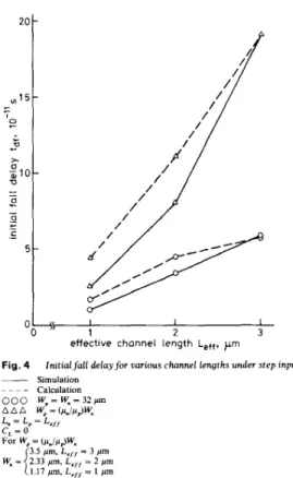
Fig. 4 shows the calculated initial fall delay t,, together with SPICE simulation results. The effective channel length for both NMOS and PMOS varies from 3 pm to 1 pm. For simplicity, the device parameters for Le,, = 1 pm are assumed to be the same as those for Le,, = 2 pm. The ratio of the aspect ratio (width/length) of
PMOS to that of NMOS is equal to unity or the ratio of their carrier mobilities. To calculate the source/drain areas, the dimension We, of the source/drain regions in the channel-length direction is assumed to be 8.5 pm for both PMOS and NMOS. We, is proportionally scaled for devices with smaller effective channel lengths. In all these cases, a general agreement between model calculations and SPICE simulations is obtained.
-
P
0.2 Y) Cf
I > U al U 0 C - - -0.1e
- / / A I I I I II
2 3effective channel length Left, prn Fig. 4 __ Simulation Calculation 000 W, = W, = 32 pm A A 4 WO = WfiPJWn L, = L, = L S f I e, = 0 For W, = (PJP~)K
Initialfall delayfor various channel lengths under step input
~ ~ _ _
3.5 pm, L,, = 3 pm
1.17 pm, L,,, = I pm
When the device dimensions are scaled down, both C , and C, of N M O S and PMOS are decreased, while I , is increased. The resultant t,, is decreased as predicted by eqn. 13 and is shown in Fig. 4. In general, a large tdJ
leads to large gate delay in CMOS logic gates.
Fig. 5 shows both calculated and SPICE-simulated initial rise delay t,,
.
A satisfactory agreement is achieved. As shown in Fig. 5, t,, is larger for L,,, = 2 pm than forLe,, = 3 pm. This is a special case due to the inherent transconductance degradation of PMOS in the adopted 2 p m CMOS process. Generally, td, decreases with a decrease in the channel length. as one compares the case of L,,, = 2 pm to that of Le,, = 1 pm.
It can be seen from Figs. 4 and 5 that the initial delays vary with the channel-width ratio Wp/Wn. Fig. 6 shows the variations of the initial fall delay, the initial rise delay
and total initial delay (t,,
+
t,,) with channel-width ratio Wp/Wn for W, = 2 pm. It is seen from Fig. 6 that the minimum initial delay of a CMOS inverter can be achieved with a suitable value of Wp/Wn. According toI
2 3
effective channel length Let,, prn
Fig. 5 Initial rise delay for various channel lengths under step input Simulation . _Calculation ~ ~ .- 000 W D = W m = 3 2 p m 4 4 A W, = IP./P,JW L, = L , = Lcf, c, = 0 For W, = Ip./p,JW. 3.5pm.Leff = 3 pm W. =
i
2.33 pm, L,,, = 2 pm 1.17 pm, Lef, = I pm I 10.3 Fig. 6different loading capacitance under step input
c, = 0.2 P
W" = 2 pm
Variations of initial delays with channel-width ratio W,/W.for
0 P . ~~~
i-.-
0 8 P L, = Ln = 2 pm 249 I E E P R O C E E D l N C S , Vol. 136, Pt. G, No. 5 , O C T O B E R 1989eqn. 13 and 15, if the variations of V,,,, and V,,,, are negligible, the optimal width ratio W,/W,, which results in the minimum total initial delay, can be approximately obtained as (WP/W",,,, 4 - VI C c $ 3 - A 0 m U - - 2 2 - f - 1 - (28) As can be seen from eqn. 28, the optimal ratio WJW. is proportional to the square root of the mobility ratio p,,/p,. This is consistent with the results of previous work 13,71.
3.2 Ramp input
Fig. 7 a shows the calculated and SPICE-simulated dependence of t,,. and t,, on W,/W, with the ramp rate K as a parameter. Good agreement is obtained. As can be seen from Fig. 7a, t d f increases, whereas t,, decreases, with the increase of WJW.. The negative dependence of
t,, on W,/W, results from the increase of Wp increasing the the drain current of MI, charging to the output node. Therefore, for a fixed value of K , there exists an optimal W&Wn such that the total initial delay (t,,.
+ rdr)
achieves a minimum value, similar to the case of step input. The resultant (t,,,.+
t d , ) is shown in Fig. 76 for different values of K . It is seen from Fig. 76 that the optimal W'/W,, resulting in the minimum (tdf+
t,,), is equal to 1.75 for all K , which is close to the value 1.78 calculated from eqn. 28. This reveals that the optimal channel-width ratio is independent of input excitations and is determined only by the device parameters as approximately expressed in eqn. 28. 5 - 4 OOL-L-+d-
2 channelwidth ratio W p l W , Fig. 78 L , = L p = 2 p m W " = 2 p m c, = I1Variations @initial fall and initial rise delays
The effect of loading capacitance C , on the initial delay is shown in Fig. 8, where SPICE-simulation results are also given for comparison. As can be seen from Fig. 8,
/
K = l x 1 0 9 V / s
-
K = 2 . 5 x 1 0 9 V / sU 2 4 6
Variations of initial delay (t
channelwidth ratio WplW, Fig. 7 8
W,,:W, Jor different ramp rate under rampd:nput
L, = Lp = 2 pm
W m = 2 s m c, = o
+ Id,) rvith channel-width ratio
U 0
_ _ _ _ _ _ _ _ - -
_ _ _ _ _ _ _ _ _ _
0 I 1 I I L 0 1 2 3 L 5 loading capacitance C,, pf Fig. 8rump rule under ramp input
Dependence of inltial deluys on loading capacitance for different
L , = Le = 2 p m W . = Z p m
w, = 4 ,cm
both t,/ and t,, increase with the increase of loading capacitance. However, the rate of increase oft,/ or t,, is not linearly proportional t o the loading capacitance. As the loading capacitance increases, the net current charg- ing to the output node is reduced, due to the increased transient current across C , , so that the output voltage overshoot
Fmox
is decreased. However, the decrease of V,,,, in turn decreases the device current I,(t) flowing out of the output node. Thus the resultant effects lead to a small increase of the initial delays when increasing the loading capacitance.It can be seen from Figs. 7 and 8 that the dominant factor in affecting the initial delays is the input ramp rate K . Fig. 9 shows the calculated and simulated variations oft,, and t,, with the value VDD/K for different values of K . Also shown in Fig. 9 are the corresponding values of input voltage
F,(q,.)
calculated from eqn. 19 (eqn. 27) at t = t,,(t,,). The initial delays increase drastically and tend to be linearly proportional to VDD/K as K decreases. However, the linear dependence of t,, and t,, on VDD/K occurs only for small values of K (slowly ramped input), as shown in Fig. 9, When the ramp rate becomes large, the feedthrough currents from input node to the output node are so large that more current I n ( t ) or I , ( t ) is needed to draw the output node to its normal state. Thus, the input must take more time to increase to a sufficient value above the threshold voltage of M I , or M I , to increase I,(tj or I p ( t ) . This can be seen from the value ofq,(y,j in Fig. 9, where Fr(VDD - V,,j increases mono- tincially beyond the threshold voltage VTn( VT,) of A410(A41p) for a large ramp rate. Therefore, only when the rising or falling time of the input voltage is very long, can the initial delays be calculated as the time at which the
I 1 I
VDD/K. ns
1 1 10
102 1
Fig. 9
corresponding input voltages w t h diferenr ramp rate under ramp input
000 simulation calculation L = L - 2 W m = 2 p m W D = 4 p m c , = o
Calculated variations of initialfall and initial rise drlars and
~~
I I p m
input voltage reaches the threshold voltage of N M O S or PMOS. Otherwise, the capacitance feedthrough effects
should be taken into account in calculating the initial delay time as considered in Section 3.1.
4 Propagation delay
In the delay time evaluation, the commonly used param- eter is the propagation delay or pair delay of a logic gate. In the characteristic waveforms [12], as shown in Fig. 10, the successive waveforms at the output nodes of interme- diate stages in a chain of identical CMOS inverters are plotted. The propagation delay t, is defined as the time interval between the successive rising or falling wave- forms at the voltage level of half-signal swings (VDD/2). Owing to the capacitive feedthrough effect, the voltage overshoot and undershoot can be clearly observed. In the characteristic waveforms, the initial fall delay t,, is defined as the time interval from the point of v(t) at which v(t) = 0 V (point A) to the point of V,,(t) at which V,,(tj = 5 V (point B). Whereas, the initial rise delay t,, is defined as the time interval from the point of Vol(t) at which K l ( t j = 5 V (point B) to the point of & ( t ) at which VJt) = 0 V (point C ) . 5 4 > 3 Q- OI
-
- P Z 1 0 time. nsFig. 10 Typical rharacteriatic wme/orms of chain of identical C M O S invrrfers together with the definilions of propagation delay and gate inilial
delar
With the specified initial delays, the sum of the initial fall delay and the initial rise delay, defined as the gate initial delay t,,, is just equal to the propagation delay t,, as verified in Fig. 11, where the propagation delay against the gate initial delay is plotted from SPICE
results for several chains of identical CMOS inverters. It
is not surprising, as shown in Fig. 11, that the propaga- tion delay is equal to the gate initial delay. When K(tj in Fig. 10 increases from 0 V, an initial fall delay is taken before the output voltage
yl(t)
decreases below V D D . Meanwhile, as V,,(t) decreases from VDD a second time, the initial rise delay is spent before Vo2(tj increases above 0 V. Since V,(tj and K2(t) are duplicate waveforms with equal rise times, the propagation delay fromy(t)
to V,,(t) therefore results from the sum of the initial fall and the initial rise delays. The smaller the gate initial delay, the smaller the propagation delay will be.Since the model developed in Section 2.2 considers the small-geometry effects in short-channel devices, it is used to calculate the delay performance of a chain of scaled CMOS inverters. In the calculations, a set of 3 gm device 251 I E E PROCEEDINGS, Vol 136, Pt G , N n 5 , OCTOBER 1989
parameters in Table 2, for both NMOS and PMOS, are scaled simultaneously in accordance with the three
1
propagation delay tp, ns Fig. 11
ohtainedfrnrn S P I C E simulations Jor various device dimensions Correlarion between gate initial delay and propagation delay
V Ipm
f P= I d s ~~.~
scaling laws: the constant-electric-field (CE), the constant-voltage (CV) and the quasiconstant-voltage
(QCV) laws [13, 141 as shown in Table 3, where s is the scaling factor. The zero-biased threshold voltages for both NMOS and PMOS are scaled in the same way as that for the power supply voltage.
Table 2 : Device parameters t o be scaled according t o scaling laws in Table 3
Parameter N M O S PMOS 3.0 3.0 0.725 7.01 E-8 0.775 2.OE16 8.7E4 0.5 0.997 820E-4 0.113 6.377E6 0.2 0.543 0.34 3.8E-4 3.6E-10 1.23E-10 1.23E-10 8.5 3.0 6 0 0.725 6.48E-8 0.85 1.75E15 6.4E4 0.5 0. 250E-4 0.295 6.024E6 0.3 0.51 5 0.341 1.2E-4 3 6E-10 1.33E-10 1.33E-10 8.5 v,,=5v
Table 3 : Three scaling laws for scaling of device parameters Scaling Constant Constant Quasi
law field voltage constant
Dimension s - ‘ s - ‘ 5-1 Voltage s - ‘ / s.o 5 S - ‘ Oxide s-’ Dopant s s s 252 voltage s - o 5 thickness
Two cases, the constant ramp rate and the scaled ramp rate, are considered. In the case of constant ramp rate, the initial delay of the first stage in Fig. 1 is calcu- lated under a fixed ramp-input excitation. In the case of scaled ramp rate, the input waveform in the characteristic waveforms case is simulated by a ramp waveform, with an appropriate ramp rate [7], to calculate the gate initial delay or propagation delay. In this case, the ramp rate of the input waveform of the present stage is also affected by the parameters of the previous stage. According to the expression of eqn. 9a, the ramp rate of the falling wave- form can be approximately expressed as
whereas that for the rising waveform is
01 I I I 1 I 0 0.2 0.4 0.6 0.8 1.0 scaling factor s-1 Fig. 12A rare K = 2 5 Y IO*V.s
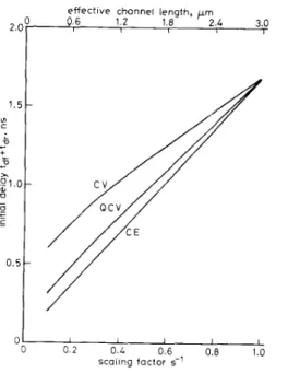
Predictions oJ initial delay ( I d ,
+
rdr) under constant rampshow the calculated dependence of the initial delay ( t d j
+
t,,) and gate initial delay t,, on the scaling factor s for constant ramp rate and scaled ramp rate, respectively. As can be seen from Fig. 12, the initial delay decreases with an increasing scaling factor s for all three scaling laws, Moreover, the linear dependence of the delays (tdJ+
td,)and t,, occurs for the CE law, which agrees with the results predicted by the conventional first-order analysis.
When the input is driven by a waveform with a con- stant ramp rate, the scaling of devices with the CE law
leads to the greatest improvement in the delay of the first stage than that with the other two laws, as can be seen IEE P R O C E E D l N G S . Vol. 136. P t . G , No. 5 , OCTOBER 1989
from Fig. 12a. Furthermore, because the large driving capability of CMOS devices is offset by the effects of a large voltage swing in the CV law, the CV law leads to the least delay improvement for constant ramp rate.
T o investigate the initial delay, a ramp input with rising or falling ramp rate equal to VDD/10 ns, VDD/20 ns,
e f f e c t i v e c h a n n e l l e n g t h . p m
0.6 1.2 1.8 2.L 3.0
1 I I I I
Fig. 13
chain o / C M O S inverters under ramp input
Experimentul output wuveform at output node of first stuge of
501
V1 I I I I
0 0.2 0.L 0.6 0.8 1.0
scaling f a c t o r 6' Fig. 12B
inoerters us function of sculrngfuctor sfor C E , CV and Q C V l a w
Cure initial delay under scaled rump rnte in chum oj CMOS
I = 1 @ d*
In the case of the characteristic waveform, however, the ramp rate of the input waveform is also affected, through eqns. 29a and 29b, by the scaling laws applied to the previous stage. Thus, in contrast to those in the con- stant ramp rate case, the reduction of gate initial delay for the QCV law is larger than that for the CE law but smaller than that for the CV law, as shown in Fig. 12h. This reveals that as one tries to improve the speed of internal circuits by the CV law, one will obtain less delay improvement in the input stage by the CV law than that by the other two laws. Therefore, the most effective manner in which to apply the scaling laws for delay improvement is to apply the CV law to the internal cir- cuits. whereas the CE law is applied to the input stage of internal circuits.
5 Experiment
Three chains of CMOS inverters were fabricated with 3 pm p-well technology. The channel lengths of both NMOS and PMOS are 3 p m , 5 p m and 8pm for the three chains. The channel width of the N M O S is 4 pm, I O pm and 16 pm and that of the corresponding PMOS is 8 pm, 20 pm or 16 pm for the three chains. Each output node of the inverter chains is connected, through a two-stage buffer, to an output pad. The dimension of the first stage of the output buffer is the same as that of the corresponding inverter chain. With a 5 V power
supply, Fig. 13 shows the measured waveform at the
output node of the first stage. It is clearly seen that the voltage overshoot and undershoot indeed occur during the transitions of input waveform.
I E E P R O C E E D I N G S , Vol. 136, P l . C , N o . 5, O C T O B E R I989 0 0 10 20 30 40 VDDIK, n s a 30
1
5 20!I
///
0 0 10 20 30 40 b VDDIK. ns Fig. 14U initial fall delay
h initial rise delay lor Y ~ O U S input ramp rates
0 ( W L), = 8,3.5 ( W . L)" = 4,3.5 ipm:pm) V I W L ) p = 16j8iW;lJn= I h ~ R ( / u m u m )
Comparisons hetween theorztrial and experimental result3
calculatmn
A ( w
up
~ 2 n i 5 w L ) n = io,5(fim,Irm)1
experiment c,, = 5 v
VDD/30 ns or VD,/40 ns was applied to the input node of the first stage, separately. The voltage waveform at the output node of the first stage was then picked up by the FET probe with 2 p f input capacitance. The parasitic capacitance between the input and output terminals due to wirings was estimated to be 0.08 pf. Taking all the factors into considerations, Figs. 14a and 146 show the calculated and experimental results of the initial fall and initial rise delays under various ramp inputs, respectively. Satisfactory agreement is obtained between the theory and experiment.
6 Conclusion
The initial delays in a C M O S inverter under step- and ramp-input excitations are characterised in detail. It is found that both the initial rise and initial fall delays determine the propagation delay of CMOS logic gates. Thus, the initial delay actually determines the speed of a logic gate. From this point of view, the initial delays are modelled for inverters with different dimensions. Optimal device dimension that results in minimum initial delay is obtained. The results are compared to those from SPICE simulations and good agreement between theoretical and SPICE-simulated results is obtained. It is shown that the capacitive feedthrough effect and thus the input slope are important factors in determing the initial delay.
Based on the model, the delay time for scaled-down CMOS inverters is calculated. As the channel length is scaled, the delay is decreased as expected. Moreover, the calculations show that the constant-voltage-scaling law is the best choice of scaling laws in reducing the propaga- tion delay of characteristic waveforms. However, for the delay response of the input stage, the constant-electric- field law is found t o be the most effective law in reducing the initial delays.
Although the analysis concentrates on CMOS
inverters only, other logic gates such as NAND, NOR, and transmission gate also have initial delays and similar modelling method can be applied accordingly.
7 References
1 MDINDL, J.D.: ‘Theoretical, practical and analogical limits in ULSI’, Int. Electron Devices Meet Tech. Dig., 1983, pp 8-13 2 WU, C.-Y., HWANG, J.-S., CHANG, C., and CHANG, C.-C.: ‘An
efficient timing model for combinational logic gates’, / E E L Trans., 1985, C A D 4 pp. 63C650
3 KUNAMA, A.: ‘CMOS circuit optimization’, Solid-state Electron., 1983.26. pp. 47-58
4 TOKUDA, T., OKAZAKI, K., SAKASHITA, K., OHKURA, I., and ENOMOTO, T.: ‘Delay-time modelling for E D MOS logic LSI’, IEEE Trans., 1983, CAD-2, pp. 129-134
5 SIMMONS, J.G., and TAYLOR, G.W.: ‘An analytic treatment of the performance of submicrometer FET Iazic’, IEEE .I.Solid-State Circuits, 1985, SC-20, pp. 1242-1251
6 AUVERGNE, D., CAMBON, G , DESCHACHT, D., ROBERT, M.. SAGNES. G.. and TEMPIER. V . : ‘Delav-time evaluation in E D MOS logic LSI’, IEEE J. Solid-state Circuits, 1986, SC-21, pp. 337-343
7 HEDENSTIERNA, N., and JEPPSON, K.O.: ‘CMOS circuit speed and buffer optimization’, IEEE Trans., 1987, CAD-6, pp. 27CL281 8 NAGEL, L.W.: ‘SPICE 2’ a computer program to simulate semi-
conductor circuits’. University of California, Berkeley, CA, USA, 1975
9 RICHMAN, P.: ‘MOS field-effect transistor and integrated circuits’ (John Wiley Inc., New York, 1973)
10 YAU, L.D.: ‘A simple theory to predict the threshold voltage of short-channel IGFETs’, Solid-State Electron., 1974, 17, pp. 1059- I063
I I ELMASRY, M.I ‘Digital MOS integrated circuits: A Tutorial’, in ‘Digital MOS Integrated Circuits’ (IEEE Press, 1981), pp. &27 12 BURNS, J.R.: ‘Switching response of complementary-symmetry
MOS transistor logic circuit’, RCA Reo., 1964, pp. 627-661 13 DANNARD, R.H., GAENSSLEN, F.H., YU. H.-N., RIDEOUT,
V.L., BASSOUS, E., and LABLANE, A.R.: ’Design of ion-implanted MOSFETs with very small physical dimensions’, IEEE J . Solid-
Stare Circuits, 1974, SC-9, pp. 256267
14 VLSI Lab., T.I. Inc.. ‘Technology and design challenges of MOS VLSI’, IEEE J. Solid-Stair Circuits, 1982, SC-17, pp. 4 4 2 4 8 15 VLADIMERSCU, A., and LIU, S.: ‘The simulation of MOS inte-
grated circuits using SPICE 2’. UCB/ERL M8017. Electronics Research Lab, University of California, Berkeley, CA, USA, 1980
8 Appendix
The Taylor’s expansion of
E(t)
around t = t,,, can be written asVAt) = K m o x
+
( t - t m , J Vb(tmax)+
( 1 - tmaJ2Vbl(t,,,)/2+
H ( t - L A (30) where H ( t - t,,,) are those of higher order terms. The boundary condition of K ( t ) is given by= VDD (31)
v b ‘ ( t m a x ) 2CVDD - % m m H ( t m a x ) I / t L z (32) Substituting eqns. 31 and 18 into eqn. 30, the second derivative of Vo(t) at I = t,,, can be written as
By neglecting the higher order terms in eqn. 32, eqn. 24b can be obtained.