IEEE ELECTRON DEVICE LETTERS, VOL. 29, NO. 11, NOVEMBER 2008 1249
Anomalous Gate-Edge Leakage Induced by
High Tensile Stress in NMOSFET
Po-Tsun Liu, Senior Member, IEEE, Chen-Shuo Huang, Peng-Soon Lim, Da-Yuan Lee,
Shueh-Wen Tsao, Chi-Chun Chen, Hun-Jan Tao, and Yuh-Jier Mii
Abstract—Anomalously high gate tunneling current, induced
by high-tensile-stress memorization technique, is reported in this letter. Carrier-separation measurement method shows that the increased gate tunneling current is originated from the higher gate-to-source/drain (S/D) tunneling current, which worsens when channel length is getting shorter. Also, the device with enhanced tensile strain exhibits 9% higher gate-to-S/D overlapping capac-itance. These data indicate that the anomalously high gate tun-neling current could be attributed to the high tensile strain that induces the effects of excessive lightly doped dopant diffusion and higher gate-edge damage. The proposed inference is confirmed by channel hot-electron stress.
Index Terms—Gate leakage current, MOSFETs, stress
memo-rization technique (SMT).
I. INTRODUCTION
T
HE INTRODUCTION of stressors to boost mobility has received a lot of attention in recent years. Stressors can be introduced in two key forms, namely, the bases of the substrate strain and the process-induced strain. The substrate-strain-based method makes use of materials with different lattice constants, such as SiGe/Si epitaxial stack to generate biaxial strain in the channel. This method introduces a global strain to the substrate. It effectively boosts mobility at the expense of higher cost [1]. On the other hand, the process-induced strain-based method provides a lower cost solution. It could appear in the forms of shallow trench isolation, contact etch-stop layer, and stress memorization technique (SMT), which introduce uniaxial strain to boost mobility [2]–[5].The introduction of strain into the channel region not only enhances the mobility of electrons and holes by altering the in-plane mass but also changes the gate tunneling current by altering the out-plane mass and SiO2/Si barrier height. How-ever, the change of strain will make a great impact on the gate tunneling current [1]. Previous articles have reported the
reduc-Manuscript received January 18, 2008; revised August 22, 2008. First published October 3, 2008; current version published October 22, 2008. This work was supported in part by the National Science Council (NSC) under Contract NSC 96-2221-E-009-130-MY3, by the MOE ATU Program, and by MOEA Technology Development for Academia Project 94-EC-17-A-07-S1-046. The review of this letter was arranged by Editor C. Bulucea.
P.-T. Liu is with the Department of Photonics and Display Institute, National Chiao Tung University, Hsinchu 30010, Taiwan, R.O.C. (e-mail: [email protected]).
C.-S. Huang is with the Institute of Electro-Optical Engineering, National Chiao Tung University, Hsinchu 30010, Taiwan, R.O.C.
P.-S. Lim, D.-Y. Lee, S.-W. Tsao, C.-C. Chen, H.-J. Tao, and Y.-J. Mii are with Taiwan Semiconductor Manufacturing Company, Hsinchu 300, Taiwan, R.O.C.
Digital Object Identifier 10.1109/LED.2008.2005518
tion of gate tunneling current by introducing the tensile strain in N-type metal–oxide–semiconductor field-effect transistor (NMOSFET) [2], [6]. In the course of boosting NMOSFET mobility using SMT with high tensile strain, the gate tunneling current was also found to be increased at the same time. This is particularly evident when the channel is driven into the accumulation mode. This observation is rather different from previous reports. In this letter, two possible factors will be investigated to analyze the anomalously high gate tunneling currents. One is the strain-induced excessive lateral dopant diffusion, and the other is the strain-induced polysilicon gate damage at the edges.
II. EXPERIMENT
The NMOSFET used in this letter was fabricated using state-of-the-art CMOS processes. The device went through the gate dielectric, gate poly, and spacer and source/drain (S/D) forma-tion [7]–[9]. The lightly doped diffusion (LDD) and S/D regions were implanted with arsenic and phosphorous, respectively. High-tensile-SMT film is then deposited, followed by high-temperature activation treatment. Process details can be found elsewhere [5]. Two NMOSFETs (Sample A and Sample B) with different strain levels were compared to investigate the effect of strain on gate tunneling current. Sample A is having a higher tensile strain than Sample B. Keithley 4200 Semi-conductor Characterization System and Agilent 4294 Precision Impedance Analyzer are the key instruments used to extract various device parameters.
III. RESULTS ANDDISCUSSION
The electrical characteristics of NMOSFET devices studied in this letter show that Sample A (with higher tensile strain) has approximately 4% higher mobility than Sample B (with lower tensile strain). The sample with higher strain also exhibits a higher drain leakage current (Id-off) at the OFF state. This is
particularly evident when the device is biased at a linear mode (Vd= 0.05 V). Electrical measurement shows that the higher Id-off is mainly contributed from the higher gate tunneling
current.
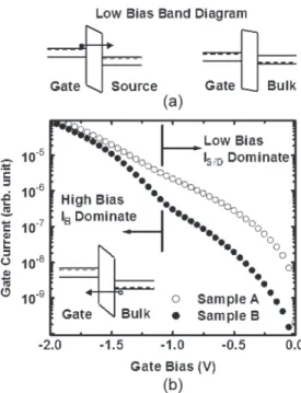
Carrier-separation measurement was performed to identify the source and the type of carriers tunneling through the gate dielectric [10]. The gate tunneling current is plotted as a func-tion of gate bias (Vg) in Fig. 1. From this plot, the measured
gate current could be divided into two distinctive regions. For the low Vg region, Sample A exhibits a much higher Jg than
Sample B. As Vg increases, the difference in Jg diminishes.
1250 IEEE ELECTRON DEVICE LETTERS, VOL. 29, NO. 11, NOVEMBER 2008
Fig. 1. Plot of gate current density (Jg) against the gate biases, extracted from
carrier-separation measurement. Sample A with higher tensile strain exhibits an anomalously high electron tunneling current (IS/D) at the low Vgregion.
(a) Gate-to-S/D is having a greater band bending than gate-to-bulk under low
Vg biasing. This explains the dominance of electron current under the low Vg region. The inset of (b) shows band bending under the higher Vg region.
The hole current from the bulk region dominates the gate current.
Fig. 2. Dependence of Jg on device channel length. The gate tunneling
current increases as channel length becomes shorter. This result could be attributed to the increase of IS/Dcomponent as the channel length is getting
shorter. The insert shows the gate-to-S/D overlap capacitance. It could be attributed to the strain-induced excessive lateral diffusion of dopants in the LDD region.
Carrier-separation measurement shows that electron and hole tunneling currents dominate at low and high gate biasing re-gions, respectively. At the low biasing region, the gate tunneling current flows primarily to the S/D regions. Sample A is found to exhibit a higher gate tunneling current than Sample B. This could be originated from the different tensile strain. It has been reported that tensile strain from an SMT is obvious, specifically at the gate edge [6], [11]. Therefore, it is reasonable to deduce that the anomalously high gate tunneling current in Sample A is a result of higher tensile strain.
Fig. 2 shows the gate tunneling current of NMOSFET de-vices as a function of channel lengths. Dede-vices were biased
Fig. 3. Linear-mode transfer characteristics for both Sample A and Sample B. Sample A with a higher tensile strain exhibits a higher Id-off. Sample B
subjected to 1000-s CHE stress (at Vg= Vd= 2.2 V) has a Id-off increase
to a level similar to that of Sample A. The results indicate that theOFF-state drain current will be increased by mechanical and electrical stresses.
at an accumulation mode. For simplicity, the gate tunneling current density was extracted at Vg=−0.75 V and shown
in Fig. 2. The results show that the gate tunneling current is a strong function of channel length. As the channel length is decreased, the impact from strain becomes more evident. The mechanical stress induced by SMT is not only originated from the vertical compressive strain or restraining polysilicon gate from the regrowth process, but it also comes from the tensile strain experienced by the S/D regime (SMT). This means that the tensile strain effect can be enhanced by both the high level of strained SMT film and channel length scaling [12], [13]. According to the experimental results, as shown in Fig. 2, the impact of SMT on gate tunneling current is signif-icant for the NMOSFET with high-tensile-SMT film and short channel.
On the other hand, it is also observed that Sample A is having approximately 9% higher gate-to-S/D overlapping capacitance than Sample B, as shown in the inset of Fig. 2. Excessive strain was reported to induce point defects, such as interstitials and vacancies in silicon. The presence of these defects assists dopant diffusion. Hence, both the tensile and compressive strain would influence the dopant diffusion behavior [14], [15]. In our samples, the LDD was implanted with arsenic. The presence of higher tensile strain in Sample A could enhance the lateral arsenic diffusion. This reasonably explains why Sample A is having a higher gate-to-S/D overlapping capacitance. The change in overlapping capacitance also increases gate tunneling current at the gate edge.
Fig. 3 shows the transfer characteristics of Sample A and Sample B in the linear mode, at a drain voltage of 0.05 V. The drain current of Sample A is higher than that of Sample B in theOFFstate. The threshold voltage of Sample A is slightly lower than that of Sample B. These results could be attributed to the effects of induced mobility increment and strain-induced lateral LDD dopant diffusion, which shortens the ef-fective channel length further. In Fig. 3, Sample B was also intentionally subjected to 1000-s channel hot-electron (CHE) stress to create damage at the proximity of the gate edge.
LIU et al.: ANOMALOUS GATE-EDGE LEAKAGE INDUCED BY HIGH TENSILE STRESS IN NMOSFET 1251
Following the CHE stresses, threshold voltage shifts positively with degradation in subthreshold swing. During hot-carrier stress, hot electrons were injected into the gate dielectric and create interface traps [16], [17]. Compared with the fresh Sample A without stress, the stressed device produces an in-creasedOFF-state drain current (Id-off), indicating that Id-off
increases when the gate edge is damaged. This verifies our inference that an excessive tensile strain at the gate edge will damage the gate edge and cause higher Id-off.
IV. CONCLUSION
This letter has shown that SMT boosts the electrical perfor-mance of NMOSFET, but the gain was achieved at the expense of a higher gate tunneling current at the OFF state. Carrier-separation measurement shows that the increased gate tunneling current is originated from the higher gate-to-S/D tunneling current, which worsens as the channel length is scaling down. Excessive strain degrades gate tunneling current via the fol-lowing two factors: 1) excessive lightly doped dopant diffusion and 2) gate-edge damage. This was verified from the higher gate-to-S/D overlapping capacitance and the hot-carrier stress study.
REFERENCES
[1] S. E. Thompson, G. Sun, Y. S. Choi, and T. Nishida, “Uniaxial-process-induced strained-Si: Extending the CMOS roadmap,” IEEE Trans.
Electron Devices, vol. 53, no. 5, pp. 1010–1020, May 2006.
[2] S. Ito, H. Namba, K. Yamaguchi, T. Hirata, K. Ando, S. Koyama, S. Kuroki, N. Ikezawa, T. Suzuki, T. Saitoh, and T. Horiuchi, “Mechan-ical stress effect of etch-stop nitride and its impact on deep submicron transistor design,” in IEDM Tech. Dig., 2000, pp. 247–250.
[3] K. Ota, K. Sugihara, H. Sayama, T. Uchida, H. Oda, T. Eimori, H. Morimoto, and Y. Inoue, “Novel locally strained channel technique for high performance 55 nm CMOS,” in IEDM Tech. Dig., 2002, pp. 27–30.
[4] G. Scott, J. Lutze, M. Rubin, F. Nouri, and M. Manley, “NMOS drive current reduction caused by transistor layout and trench isolation induced stress,” in IEDM Tech. Dig., 1999, pp. 827–830.
[5] C. H. Chen, T. L. Lee, T. H. Hou, C. L. Chen, C. C. Chen, J. W. Hsu, K. L. Cheng, Y. H. Chiu, H. J. Tao, Y. Jin, C. H. Diaz, S. C. Chen, and M.-S. Liang, “Stress memorization technique (SMT) by selectively strained-nitride capping for sub-65 nm high-performance strained-Si device application,” in VLSI Symp. Tech. Dig., 2004, pp. 56–57.
[6] A. Eiho, T. Sanuki, E. Morifuji, T. Iwamoto, G. Sudo, K. Fukasaku, K. Ota, T. Sawada, O. Fuji, H. Nii, M. Togo, K. Ohno, K. Yoshida, H. Tsuda, T. Ito, Y. Shiozaki, N. Fuji, H. Yamazaki, M. Nakazawa, S. Iwasa, S. Muramatsu, K. Nagaoka, M. Iwai, M. Ikeda, M. Saito, H. Naruse, Y. Enomoto, Kitano, S. Yamada, K. Imai, N. Nagashima, T. Kuwata, and F. Matsuoka, “Management of power and performance with stress memorization technique for 45 nm CMOS,” in VLSI Symp.
Tech. Dig., 2007, pp. 218–219.
[7] C. H. Chen, Y. K. Fang, S. F. Ting, W. T. Hsieh, C. W. Yang, T. H. Hsu, M. C. Yu, T. L. Lee, S. C. Chen, C. H. Yu, and M. S. Liang, “Downscaling limit of equivalent oxide thickness in formation of ultrathin gate dielectric by thermal-enhanced remote plasma nitridation,” IEEE Trans. Electron
Devices, vol. 49, no. 5, pp. 840–846, May 2002.
[8] A. E. Islam, G. Gupta, S. Mahapatra, A. T. Krishnan, K. Ahmed, F. Nouri, A. Oates, and M. A. Alam, “Gate leakage vs. NBTI in plasma nitrided oxides: Characterization, physical principles, and optimization,” in IEDM
Tech. Dig., 2006, pp. 1–4.
[9] K. L. Cheng, C. C. Wu, Y. P. Wang, D. W. Lin, C. M. Chu, Y. Y. Tarng, S. Y. Lu, S. J. Yang, M. H. Hsieh, C. M. Liu, S. P. Fu, J. H. Chen, C. T. Lin, W. Y. Lien, H. Y. Huang, P. W. Wang, H. H. Lin, D. Y. Lee, M. J. Huang, C. F. Nieh, L. T. Lin, C. C. Chen, W. Chang, Y. H. Chiu, M. Y. Wang, C. H. Yeh, F. C. Chen, C. M. Wu, Y. H. Chang, S. C. Wang, H. C. Hsieh, M. D. Lei, K. Goto, H. J. Tao, M. Cao, H. C. Tuan, C. H. Diaz, and Y. J. Mii, “A highly scaled, high performance 45 nm bulk logic CMOS technology with 0.242 μm2 SRAM cell,” in IEDM Tech. Dig., 2007,
pp. 243–246.
[10] Y. Shi, T. P. Ma, S. Prasad, and S. Dhanda, “Polarity dependent gate tun-neling currents in dual-gate CMOSFETs,” IEEE Trans. Electron Devices, vol. 45, no. 11, pp. 2355–2360, Nov. 1998.
[11] L. S. Adam, C. Chiu, M. Huang, X. Wang, Y. Wang, S. Singh, Y. Chen, H. Bu, and J. Wu, “Phenomenological model for ‘stress memorization’ effect from a capped-poly process,” in Proc. SISPAD, 2005, pp. 139–142. [12] C. Ortolland, P. Morin, C. Chaton, E. Mastromatteo, C. Populaire, S. Orain, F. Leverd, P. Stolk, F. Boeuf, and F. Arnaud, “Stress memo-rization technique (SMT) optimization for 45 nm CMOS,” in VLSI Symp.
Tech. Dig., 2006, pp. 78–79.
[13] X. Z. Bo, L. Kang, T. Luo, K. Junker, S. Zollner, G. Spencer, V. Kolagunta, and J. Cheek, “High performance NMOS transistors for 45 nm SOI technologies,” in Proc. IEEE Int. SOI Conf., 2007, pp. 15–16. [14] Y. M. Sheu, S. J. Yang, C. C. Wang, C. S. Chang, L. P. Huang, T. Y. Huang, M. J. Chen, and C. H. Diaz, “Modeling mechanical stress effect on dopant diffusion in scaled MOSFETs,” IEEE Trans. Electron Devices, vol. 52, no. 1, pp. 30–38, Jan. 2005.
[15] P. R. Chidambaram, C. Bowen, S. Chakravarthi, C. Machala, and R. Wise, “Fundamentals of silicon material properties for successful exploitation of strain engineering in modern CMOS manufacturing,” IEEE Trans.
Electron Devices, vol. 53, no. 5, pp. 944–964, May 2006.
[16] T. Wang, L. P. Chiang, N. K. Zous, C. F. Hsu, L. Y. Huang, and T. S. Chao, “A comprehensive study of hot carrier stress-induced drain leakage current degradation in thin-oxide n-MOSFETs,” IEEE Trans.
Electron Devices, vol. 46, no. 9, pp. 1877–1882, Sep. 1999.
[17] E. Li, E. Rosenbaum, L. F. Register, J. Tao, and P. Fang, “Hot carrier induced degradation in deep submicron MOSFETs at 100◦C,” in Proc.