Compact Planar Quasi-Elliptic Function Filter With
Inline Stepped-Impedance Resonators
Jen-Tsai Kuo, Senior Member, IEEE, Ching-Luh Hsu, and Eric Shih
Abstract—Compact microstrip bandpass filters of orders = 4 6 and 8 with quasi-elliptic function responses are synthesized with inline stepped-impedance resonators. The filters have enhanced transition responses since two transmission zeros are generated on both sides of the passband. Existence of these two zeros is investigated by formulating the -matrix of the equiv-alent circuit for the filter and taking adjacent and nonadjacent coupling into account. Some matrix elements +2representing coupling between two nonadjacent resonators are shown to have the opposite signs in both the lower and upper sides of the center frequency. This property leads to creation of the two transmission zeros on both sides of the passband. It is demonstrated that one more zero can be created in the rejection band by the tapped-line input/output scheme. Experimental circuits on substrates with = 2 2 and 10 2 are measured to validate the theory and design.
Index Terms—Bandpass filter, elliptic function response, inline, stepped-impedance resonator, transmission zero.
I. INTRODUCTION
I
N THE RF front-ends of recent wireless communication sys-tems, bandpass filters are required to have several essential properties, such as high selectivity, wide upper stopband, and compact circuit size. Based on the traditional parallel-coupled configuration [1], [2], however, the circuit may become very long since an th-order filter consists of a cascade of sections. To tackle this problem, folded stepped-impedance res-onator filters are proposed to reduce the circuit size [3], [4]. Generally speaking, the stepped-impedance resonators are suit-able for designing filters with a good transition response and an extended rejection band since its first higher order resonance can be easily tuned to much higher than twice the fundamental frequency. To enhance filter performance in the transition and rejection bands, however, one of the most effective ways is to insert transmission zeros. The insertion can be realized by the cross coupling [5], [6] or the source–load coupling [7], [8].In this paper, we explore a simple filter structure using stepped-impedance resonators as building blocks. Fig. 1 plots two fourth-order circuits with both symmetric and
Manuscript received February 4, 2007; revised April 25, 2007. This work was supported in part by the Ministry of Education under the ATU Program and by the National Science Council, Taiwan, R.O.C., under Grant NSC 95-2221-E-009-037 and Grant NSC 95-2752-E-009-003-PAE.
J.-T. Kuo and C.-L. Hsu are with the Department of Communication Engi-neering, National Chiao Tung University, Hsinchu, 300 Taiwan, R.O.C. (e-mail: [email protected]).
E. Shih is with Foxconn Electronics Inc., Hsinchu, 300 Taiwan, R.O.C. Color versions of one or more of the figures in this paper are available online at http://ieeexplore.ieee.org.
Digital Object Identifier 10.1109/TMTT.2007.901604
Fig. 1. Two inline fourth-order filters with two tapped input/output schemes: symmetric(A–B) and skew–symmetric (A–B ) feeds.
skew-symmetric feeds [4]. The circuit exhibits several attrac-tive properties, such as compact size, wide upper stopband, elliptic function passband response, and plural transmission zeros. In Fig. 1, all resonators form an inline array so that the circuit occupies a compact area. When order is increased, the circuit size grows only in the direction of the width, which is usually much smaller than the length of the resonator. Besides, in the array, adjacent and nonadjacent coupling simultaneously exists among the resonators. Although the analysis becomes more complicated, creation of certain transmission zeros in the filter response indeed relies on nonadjacent coupling.
In the combline design [9]–[11], grounded line sections of different lengths are loaded with various capacitors. It can be easily identified in Fig. 1 that at the fundamental resonance, the low- and high- segments of the resonator behave as ca-pacitors and inductors, respectively. Although the circuit layout looks quite similar to that of a combline structure, it has at least several distinct features. First, all the resonators have identical geometry and exhibit an electric length of 180 at the design frequency. Second, multiple coupling exists among the low-section array, as well as the high- array. Third, the circuit needs neither a lumped element, nor grounding via so that filter fabrication is easier and more reliable. The price paid for the full-length resonators is that the circuit area is slightly larger than twice the size of a quarter-wave combline counterpart [10]. The use of full-length resonators, however, brings one more de-gree of freedom to circuit designers in choosing symmetric or skew-symmetric feed [4]. It will be shown later that existence and location of certain zeros are subject to the symmetry used in the tapped input/output arrangement.
Here, we limit ourselves to exploring inline stepped-impedance resonator filters only of orders four, six, and eight. Some results for circuits of lower orders can be referred to [12], [13]. In [12], second-order filters are developed to achieve a wide upper stopband. The circuit in [13] also possesses a quasi-elliptic function response. Its analysis by the theory of multiple coupled microstrips, however, lacks for a design concept for filter synthesis. This paper is organized as follows. Section II briefly describes the passband synthesis procedure
of a -parameter matrix by taking the adjacent and nonadjacent coupling into account. Section IV addresses the creation of zero by the tapped input/output structure, Section V presents measured results for three experimental circuits. Section VI draws the conclusion.
II. PASSBANDSYNTHESIS
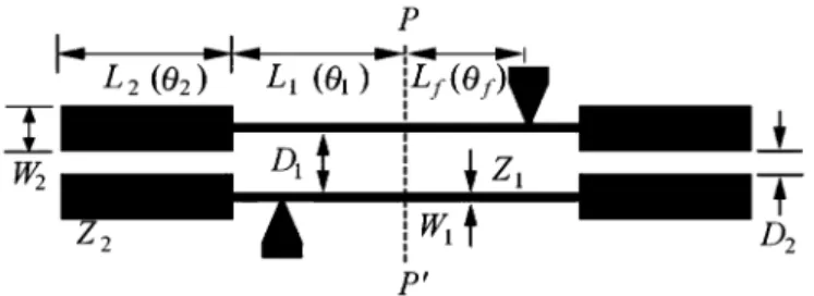
Fig. 2 shows the generic basic coupling structure for the fil-ters in Fig. 1. Each resonator has one high- and two low- sec-tions. The former has physical (electric) lengths and each of the later has , and their respective widths are and with corresponding characteristic impedances and
. In addition to , the gap size can be tuned to establish necessary coupling for synthesizing the passband. Choice of the geometrical dimensions for the resonator has been extensively studied in [1] and [2]. The impedance ratio and length ratio are the key parameters to deter-mine its resonant spectrum. If and are properly chosen, the first spurious resonance can be pushed far beyond twice the fun-damental frequency or [2]. For example, if the first higher order resonance occurring at is desired, and
can be used. When GHz, geometry parameters can be mm, mm, and mm for a substrate with and thickness mm.
The next step is to determine spacing between each pair of adjacent resonators. The coupling coefficient between the th and th resonators, i.e., , is given by [14]
(1) where is the th element value of the low-pass filter prototype and is the fractional bandwidth. To realize this coefficient for coupled resonators in Fig. 2, the test method in [6] can be invoked. Through weak gap feeds to the coupled resonators, the simulated transmission response will present two peaks. If the peaks are at and , the coefficient can be calculated as
(2) For the fourth-order circuits in Fig. 1, the coupling matrix is symmetric about its two main diagonals, i.e.,
and . Thus, only and need specifying since all diagonal entries are zero and is negligible owing to the relatively large space between resonators 1 and 4.
Fig. 3. Coupling coefficients of two stepped-impedance resonators againstD for variousD . L = L = 7:6; W = 0:4; W = 2:0 (all in millimeters). Substrate:" = 2:2; thickness = 0:508 mm.
It can be anticipated that change of will not significantly alter the first resonance of the resonator, but will change mag-nitude, and even polarity of the coupling coefficient of two coupled resonators. This property is useful for adjusting the resonator geometry when more than one coupling coefficients have to be simultaneously considered in filter synthesis. An ex-ample will be given in Section V for such a demonstration. For mm to , Fig. 3 plots coupling coefficients of two resonators against . Except for , each curve runs from positive to negative values when is increased up to 4 mm. Generally speaking, the structure consists of both electric and magnetic coupling, called mixed coupling in [6]. When is small, magnitude of magnetic coupling due to current on the thin sections is larger than that of electric coupling between the low- sections at both ends. When is increased to be large enough for small , on the other hand, electric coupling becomes dominant. The coefficient calculated by (2) is the net coupling, which can be electric or magnetic .
The use of curves in Fig. 3 can be demonstrated as follows. Suppose we are designing a fourth-order Chebyshev filter with a 0.1-dB ripple and %. From (1), the three interstage coupling coefficients are and
. If mm is chosen, we have
, and the zero-crossing point is at mm. It is obvious that both electric and magnetic coupling can be used to realize each value. Thus, there are at least two possible designs: one uses and , and the other uses and . The former and latter are, respectively, referred to as the - and -type filters herein.
For the input and output coupling, the tap positions, i.e., in Fig. 2, should be determined by matching the singly loaded
of the tapped resonator with the passband specification [15]. The singly loaded is defined as
dB
(3) where is the impedance seen by the resonator looking to-ward the source, is the operation frequency, and is the input susceptance of the resonator seen at the tap point. The
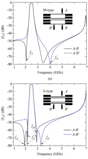
Fig. 4. Simulation responses of the two fourth-order filters. (a)M-type: D = D = 0:28; D = 1:0; L = 3:2. (b) E-type: D = D = 0:82; D = 0:37; L = 3:2 (all in millimeters).
derivation of (3) for a stepped-impedance resonator can be re-ferred to [2]. Both - and -type circuits can be designed with the symmetric or the skew-symmetric feeds [4] with identical values and, hence, identical passband re-sponses. In the rejection bands, nevertheless, they exhibit quite different characteristics. Fig. 4 shows the simulated re-sponses of the fourth-order - and -type filters. The four passbands, say, before dB, show very good agree-ment. In Fig. 4(a), both the -type filters have a transmission zero in the upper stopband. The circuit with the symmetric feed, however, has one more zero in the lower stopband. In Fig. 4(b), the two -type filters exhibit sharp tran-sition bands, like those of an elliptic function response, since two zeros, i.e., and , are created on both sides of the passband. In addition, there is an extra transmission zero in the lower stopband and in the upper stopband for the
and feeds, respectively. Obviously, the -type filters possess better frequency selectivity in the stopband than the -type ones. Thus, the -type filters are investigated in de-tail as follows.
III. TRANSMISSIONZEROS OF THE -TYPEFILTERS
The resonators of a cross-coupled four-pole filter [4]–[6], [16] are arranged in a 2 2 configuration to achieve a quasi-elliptic
Fig. 5. (a) Two coupled resonators with coupling. (b) Equivalent circuit.
function response. The occurrence of the zeros relies on the elec-tric coupling , which causes two split signals to be out-of-phase at the output port. In the -type filters, however, the el-liptic function-like response is clearly resulted from a different scheme since the in Fig. 1 can be negligible, while the non-adjacent coupling coefficients and should be taken into account. In addition, for predicting the zeros of the particular filter configuration, based on the -parameter of the equivalent circuit of the filter, an analysis method is developed as follows. The equivalent lumped-circuit model of two coupled res-onators in Fig. 5(a) is shown in Fig. 5(b). Each resonator is modeled with a parallel LC network, and there are magnetic and electric coupling between the inductors and capacitors, re-spectively. From the circuit theory, the two-port -parameters can be derived as follows:
(4) (5) where (6) (7) (8) (9) (10) (11) The coefficients in (9) and in (10), respectively, repre-sent magnetic and electric coupling between the two resonators. They are assumed constants over a certain frequency range cen-tered at the design frequency. The natural frequencies and in (2) of the coupled system can be determined by two condi-tions: , which are obtained by enforcing the
elements are usually assumed independent of frequency [6]. For investigating the possible occurrence of transmission zeros, de-fine the relative phase between and as
(13)
It can be deduced from this equation that when or , and when if
(i.e., net coupling is magnetic) or
if (i.e., net coupling is electric). The identification rule for determining the type of coupling proposed in [17] can also be justified by (13) as well.
Fig. 6 plots the simulated responses for the three basic cou-pled structures of the -type filter in Fig. 4(b). The -param-eters are obtained by Zeland Software Inc.’s software package IE3D [18]. Each response shows a jump at due to the phase change of the denominator of (13). Based on Fig. 6(a), one can assure that the coupling between resonators 1 and 2 is mag-netic dominant and for 2 GHz GHz. Similarly, the response in Fig. 6(b) guarantees . In Fig. 6(c), there are extra phase jumps at 2.08 and 2.75 GHz. Two important properties of this coupled structure should be identified by the latter jump. First, the type of coupling is magnetic, as indicated in Fig. 6(a). The jump at GHz indicates that changes sign, by (13), since when . Also, by (13), the and values can be extracted since and is known by (2) from simulation data. The jump at 2.08 GHz, however, cannot be ex-plained by (13). It could be due to the fact that the equivalent circuit in Fig. 5(b) has a lower frequency limit for modeling the distributed coupled resonators with a relative large distance in Fig. 6(c).
Identifying the type of coupling and value of is further investigated for mm and mm by Fig. 7. From Fig. 7(a), is electric coupling and . Sim-ilarly, Fig. 6(b) indicates that is of the magnetic type and . It is important to identify and from the responses of coupled resonators in Figs. 6(c) and 7 since analysis of the transmission zeros relies on it. By analyzing the
Fig. 6. Responses of Y 0 Y for investigating occurrence of the trans-mission zeros of theE-type filter in Fig. 4(b). (a) Resonators 1 and 2, D = 0:82 mm. (b) Resonators 2 and 3, D = 0:37 mm. (c) Resonators 1 and 3, D = 3:19 mm.
Fig. 7. Y 0 Y responses for identification type of coupling between resonators 1 and 3. (a)D = 0:6 mm. (b) D = 1:5 mm.
phase relation of two split signals in the main and cross-coupled paths, a zero in the upper stopband can occur at GHz [17]. This zero can also be validated by the -matrix method given below. Let the filter bandwidth % and ripple dB, and then the external . The -matrix for the circuit, normalized with respect to can be expressed
Fig. 8. jS j responses based on coupling matrices in (14).
as
(14)
where and . These values are derived from (1). The entries in the first off-diagonal use the following approximation. For example,
since and the last term in (7) is neglected. Values of and can be obtained by prescribed zeros at . If the two zeros are symmetric about is required. Note that the sign of the elements is determined by
. When and , and can be obtained from the responses based on (14), respec-tively. Fig. 8 shows responses from the matrices with and without the nonadjacent coupling . Note that when , the response will have no transmission zero. It can be seen from this example that values of and can be varied for controlling these two transmission zeros. One possible way to adjust and is to slide or deform the high- section of one of the coupled resonators, as shown in Fig. 1.
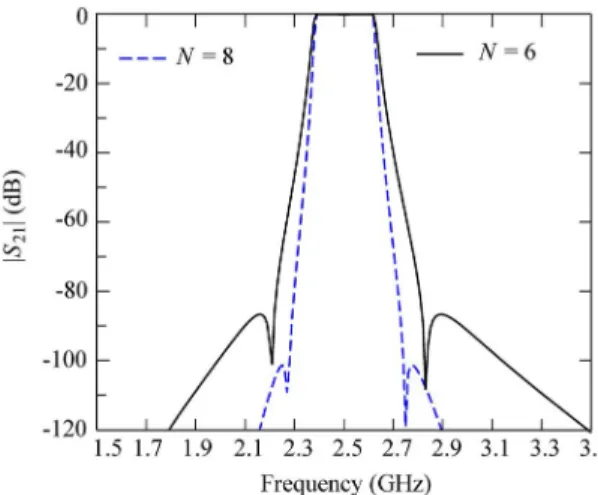
Fig. 9. Responses of higher order inline filters withm = e = 0:011.
The -matrix in (14) can be easily extended to circuits of order and with the quasi-elliptic response. The -ma-trix can be established and the frequencies of the zeros can be predicted. For example, the coupling matrix for is shown in (15) at the bottom of this page, where
and , and . Fig. 9 plots the responses for filters of order and with GHz, %, and a 0.1-dB ripple. For all nonadjacent elements
is used.
IV. TRANSMISSIONZEROSDUE TOTAPPEDINPUT/OUTPUT
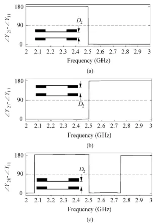
Fig. 10 plots simulation responses of the -type fil-ters with skew-symmetric feed for and mm. Impedance transformers are added to keep the value of each tapped resonator unchanged for the three tap positions. It can be seen that frequencies of and , as well as the passband do not vary significantly with the changes of . However, the zero moves to higher frequency when tap point is moved away from the center to the edge of the resonator. It reflects the fact that determination of can be dominated by . In the par-allel-coupled stepped-impedance resonator filters in [2], a zero can be created at a frequency where the electric length of the arm between the open end of the tapped resonator and the tap point is one quarter-wavelength long. The arm used for coupling with an adjacent resonator, however, does not create a zero. For
Fig. 10. Moves of the tunable transmission zeros due to the slide of tap point for theE-type filters with skew-symmetric feed.
Fig. 11. Analysis off and f . (a) Four-port network. (b) Responses for X of theE-type filters. For 0(X ) , only the important part is shown.
the structure in Fig. 1, both open ends of the input and output resonators are coupled with their adjacent resonators. Thus, cre-ation of the zero in Fig. 10 needs further investigation.
The four-port network in Fig. 11(a) is employed for the pre-diction. Two more ports are added to the circuit in Fig. 1 since, in analysis, the whole circuit can be reduced by half due to the symmetry (dashed line). Let be the total current flowing into port or . It can be derived that
(16) where subscript represents symmetric feed and and denote that the dashed line is a magnetic and electric wall, respectively. For the skew-symmetric feed, and in
(c)
Fig. 12. X responses for the test circuit and the E-type circuit. (a) Test cir-cuit. (b) Skew-symmetric feed. (c) Symmetric feed.
Fig. 11(a) are set to zero. The transfer impedance , denoted as , can be written as
(17) For both feeds, zeros of the responses can be obtained by enforcing (16) and (17) to zero. The conditions are
(18) where the plus and minus signs apply to the skew-symmetric and symmetric feeds, respectively. Obviously, complete formulas of and will be tedious and complicated since four-microstrip structures are involved [13].
The transfer impedances are purely reactive for lossless struc-tures. Let the reactance be denoted by and . Simulated and responses are shown in Fig. 11(b), where each intersection point indicates a zero in the response. Note that the zeros and are in the lower and upper rejection bands for the symmetric and skew-symmetric feeds, respectively. To further investigate the property of the zeros, the behavior of the circuit in Fig. 12(a) is tested. It is the -type filter in Fig. 4(b) that is altered by
Fig. 13. Group delay andS-parameter responses of the E-type filters with symmetric feed. All circuit parameters are in Fig. 4(b).
Fig. 14. Layout and performances of theE-type filters with skew-symmetric feed. (a) Circuit layout. Dimensions in millimeters: L = 3:48; L = 3:78; L = 2:2; L = 1:48; L = 4:1; L = 1:5; L = 2:13; W = 0:2; W = 2:5; D = 0:6; D = 0:5. (b) Group delay, jS j and jS j responses.
moving the high- sections of resonators 1 and 4 outward. Fig. 12(b) and (c) plots the responses of the test circuit (solid lines) and the -type filter (dashed lines). It can be seen that the -type filter shows three transmission zeros. For the test circuit, however, both and disappear, although and exist, respectively, for symmetric and skew-symmetric feeds. Based on the results in Fig. 12(b) and (c), must be negative or must be capacitive in the transition bands for creation of and in the design of the -type filters.
Fig. 15. Layout and performances of the sixth-orderE-type filters with skew-symmetric feed. (a) Circuit layout. Dimensions in millimeters:L = L = 6:32; L = 3:2; W = 0:2; W = 2:5; D = D = 0:14; D = D = 0:82; D = 0:23. (b) Group delay, jS j and jS j responses.
V. SIMULATION ANDMEASUREMENT
Fig. 13 plots the simulation and measured responses of the -type filters with a symmetric feed. All geometric parameters are referred to Fig. 4(b). The tap points are chosen to match to the value for 50- reference impedance. The measured re-jection levels are better than 40 dB up to 5 GHz or . The extra zero is at 1.9 GHz. It is found that rejection levels of better than 60 dB can be achieved within the bands covering from 1.82 to 2.18 and 2.9 to 3.01 GHz. It can be observed that has a response with sharp transition bands and good sym-metry about the center frequency. The measured and simulated group delays are also given.
The second design demonstrates control of the transmission zeros and . The center frequency GHz and fractional bandwidth % with a 0.1-dB ripple level. Let GHz and GHz, the coupling
co-efficients and
. The geometric dimensions of the end resonators and the tap position are chosen to locate the zero at with no transformer. For reducing the circuit size, a substrate with and thickness mm is used. Fig. 14(a) shows the circuit layout with deformed resonators 2 and 3 to simultane-ously fulfill required magnitudes of all the coupling coefficients including and . To have , the high- sections of two middle resonators are bent to a U shape. The distance can be readily determined by the results shown in Fig. 3. At the same time, the low- sections are moved inwardly by a distance to simultaneously realize the specified and values. It could be due to the right-angled bends in the
high-tric and magnetic types of coupling for establishing all coupling coefficients with proper magnitudes and phases. Note that the coupling coefficients and are of an electric type. Simulation and measured results with a skew-symmetric feed are plotted in Fig. 15. The insertion loss is 2.5 dB at , in-band return loss is better than 15 dB, and the stopband with a rejec-tion level of 50 dB is extended to 7.5 GHz and 30 dB to 12.5 GHz .
An eighth-order filter is synthesized with a skew-symmetric feed. The circuit simulation exhibits a similar response to that of a sixth-order -type filter in Fig. 15, but has better rejection rates in transition bands.
VI. CONCLUSION
Stepped-impedance resonators have been arranged in an in-line configuration to make the entire circuit a compact size. The use of the resonators has assured a wide upper stopband and the inline resonator array facilitates new coupling schemes for pro-ducing a quasi-elliptic function passband response. Creation of transmission zeros has been investigated by -matrix parame-ters of the equivalent circuit of the filter. It has been shown that proper nonadjacent elements are key factors for creating the transmission zeros on both sides of the passband for fourth-, sixth-, and eighth-order filters. An enhanced attenuation rate in transition bands can then be obtained. Formulation of the con-ditions of the extra zero in rejection bands has also been given. It has been demonstrated for the particular inline structure that the extra zero can be placed in the lower and upper stopbands by symmetric and skew-symmetric feeds, respectively. For demon-strative purposes, measured results for three experimental filters have been compared with simulation data.
REFERENCES
[1] M. Makimoto and S. Yamashita, “Bandpass filters using parallel cou-pled stripline stepped impedance resonators,” IEEE Trans. Microw.
Theory Tech., vol. MTT-28, no. 12, pp. 1413–1417, Dec. 1980.
[2] J.-T. Kuo and E. Shih, “Microstrip stepped-impedance resonator band-pass filter with an extended optimal rejection bandwidth,” IEEE Trans.
Microw. Theory Tech., vol. 51, no. 5, pp. 1554–1559, May 2003.
[3] M. Sagawa, K. Takahashi, and M. Makimoto, “Miniaturized hairpin resonator filters and their application to receiver front-end MIC’s,”
IEEE Trans. Microw. Theory Tech., vol. 37, no. 12, pp. 1991–1997,
Dec. 1989.
[4] C.-M. Tsai, S.-Y. Lee, and C.-C. Tsai, “Performance of a planar filter using a 0 feed structure,” IEEE Trans. Microw. Theory Tech., vol. 50, no. 10, pp. 2362–2367, Oct. 2002.
Theory Tech., vol. 50, no. 4, pp. 1216–1219, Apr. 2002.
[11] W. Menzel and M. Berry, “Quasi-lumped suspended stripline filters with adjustable transmission zeros,” in IEEE MTT-S Int. Microw. Symp.
Dig., Fort Worth, TX, Jun. 2004, pp. 1601–1604.
[12] C.-L. Hsu and J.-T. Kuo, “A two-stage SIR bandpass filter with an ultra-wide upper rejection band,” IEEE Microw. Wireless Compon. Lett, vol. 17, no. 1, pp. 34–36, Jan. 2007.
[13] E. Shih and J.-T. Kuo, “A new compact microstrip stacked-SIR bandpass filters with transmission zeros,” in IEEE MTT-S Int. Microw.
Symp. Dig., Philadelphia, PA, Jun. 2003, pp. 1077–1080.
[14] G. L. Matthaei, L. Young, and E. M. T. Jones, Microwave Filters,
Impedance-Matching Network, and Coupling Structures. Norwood, MA: Artech House, 1980, ch. 8, p. 432.
[15] J. S. Wong, “Microstrip tapped-line filter design,” IEEE Trans. Microw.
Theory and Tech., vol. MTT-27, no. 1, pp. 44–50, Jan. 1979.
[16] C.-L. Hsu and J.-T. Kuo, “Design of cross-coupled quarter-wave SIR filters with plural transmission zeros,” in IEEE MTT-S Int. Microw.
Symp. Dig, San Francisco, CA, Jun. 2006, pp. 1205–1208.
[17] C.-C. Chen, Y.-R. Chen, and C.-Y. Chang, “Miniaturized microstrip cross-coupled filters using quarter-wave or quasi-quarter-wave res-onators,” IEEE Trans. Microw. Theory Tech., vol. 51, no. 1, pp. 120–131, Jan. 2003.
[18] IE3D Simulator. Zeland Softw. Inc., Freemont, CA, Jan. 2002.
Jen-Tsai Kuo (S’88–M’92–SM’04) received the Ph.D. degree from the Institute of Electronics, National Chiao Tung University (NCTU), Hsinchu, Taiwan, R.O.C., in 1992.
Since 1984, he has been with the Department of Communication Engineering, NCTU, where he is currently a Professor. From 1995 to 1996, he was a Visiting Scholar with the Electrical Engineering Department, University of California at Los Angeles (UCLA). His research interests include analysis and design of microwave integrated circuits (MICs) and numerical techniques in electromagnetics.
Dr. Kuo was the recipient of the 2006 Thomson Scientific Citation Laureate Award.
Ching-Luh Hsu received the B.S. degree in com-munication engineering from National Chiao Tung University (NCTU), Hsinchu, Taiwan, R.O.C., in 1989, the M.S. degree in electrical engineering from National Sun Yet-Sen University (NSYSU), Kaohsiung, Taiwan, R.O.C., in 1994, respectively, and is currently working toward Ph.D. degree at NCTU.
From 1994 to 1999, he was a RF Engineer with Microelectronic Technology Incorporation (MTI), where he developed transceivers for point-to-point digital microwaves. In 1999, he joined the faculty of the Department of Elec-tronic Engineering, Ta Hwa Institute of Technology, Hsinchu, Taiwan, R.O.C., where he is currently a Lecturer. His research interests include the design of planar circuits for microwave and millimeter-wave applications.
Eric Shih was born in Taoyuan, Taiwan, R.O.C., on April 12, 1976. He received the B.S. degree in engineering and system science from National Tsing Hua University (NTHU), Hsinchu, Taiwan, R.O.C., in 1998, and the Ph.D. degree in communication engineering from National Chiao Tung University (NCTU), Hsinchu, Taiwan, R.O.C., in 2003.
He is currently with Foxconn Electronics Inc., Hsinchu, Taiwan, R.O.C. His research interests include the design of microwave planar filters, RF modules, and antennas for microwave and mil-limeter-wave applications.