1092 IEEE TRANSACTIONS ON ELECTRON DEVICES, VOL. 60, NO. 3, MARCH 2013
Design and Analysis of Robust
Tunneling FET SRAM
Yin-Nien Chen, Ming-Long Fan, Student Member, IEEE, Vita Pi-Ho Hu, Member, IEEE,
Pin Su, Member, IEEE, and Ching-Te Chuang, Fellow, IEEE
Abstract—With a steep subthreshold slope, tunneling FETs (TFETs) are promising candidates for ultralow-voltage operation compared with conventional MOSFETs. However, the delayed saturation characteristic and the broad soft transition region result in a large crossover region/current in an inverter, thus degrading the hold/read static noise margin (H/RSNM) of TFET SRAM cells. The write-ability and write static noise margin (WSNM) of TFET SRAM cells are constrained by the uni-directional conduction characteristics and large crossover con-tention of the write access transistor and the holding transistor. In this paper, we present a detailed analysis of TFET circuit switching/output characteristics/performance and the underlying physics. The stability/performance of several TFET SRAM cells are then analyzed/compared using atomistic technology computer-aided design mixed-mode simulations. Finally, a robust 7T driver-less (DL) TFET SRAM cell is proposed. The proposed 7T DL TFET SRAM cell, with better output characteristics in single-gate mode, and decoupled read current path from cell storage node and push–pull write action with asymmetrical raised-cell-virtual-ground write-assist, provides a significant improvement in hold, read, and write stability and performance.
Index Terms—Band-to-band tunneling, output characteristic, SRAM, tunnel FET (TFET).
I. INTRODUCTION
V
OLTAGE scaling is an efficient way to achieve ultralow-power consumption of circuits. However, due to the fundamental limit of the subthreshold swing of the MOSFET device (60 mV/dec at 300 K), continual reduction of the supply voltage causes dramatic degradation of the Ion/Ioffratio andin-crease of the leakage current in the MOSFET device. Recently, the tunneling FET (TFET), which utilizes the band-to-band tunneling as the conduction mechanism, has emerged as one of the most promising candidates for ultralow-voltage/power oper-ation [1]–[3]. Several studies on the TFET device demonstrat-ing the progress of fabrication and experimental results have been reported [4]–[7]. However, one of the major application constraints of the TFET is the unidirectional current-conduction
Manuscript received August 23, 2012; revised October 24, 2012 and December 5, 2012; accepted January 4, 2013. Date of publication February 4, 2013; date of current version February 20, 2013. This work was supported in part by the National Science Council of Taiwan under Contract NSC 101-2221-E-009-150-MY2, by the Ministry of Economic Affairs in Taiwan under Contract 100-EC-17-A-01-S1-124, and by the Ministry of Education in Taiwan under the Aim for the Top University Program. The review of this paper was arranged by Editor Y.-H. Shih.
The authors are with the Department of Electronics Engineering and the Institute of Electronics, National Chiao Tung University, Hsinchu 30010, Taiwan (e-mail: [email protected]).
Color versions of one or more of the figures in this paper are available online at http://ieeexplore.ieee.org.
Digital Object Identifier 10.1109/TED.2013.2239297
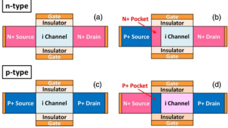
Fig. 1. Structures of the (a) n-type MOSFET, (b) n-type p-n-p-n TFET, (c) p-type MOSFET, and (d) p-type p-n-p-n TFET.
characteristic. For pass-transistor-based logic circuits, a TFET with an opposite current-conducting direction can be added at the expense of area/performance if bidirectional characteris-tic is required. For SRAM cells, however, the unidirectional characteristics severely impact robustness due to conflicting read/write requirements and the stringent cell-area constraint [8]–[10]. In this paper, we present a detailed analysis of TFET circuit switching/output characteristics/performance and com-pare the stability/performance of several TFET SRAM cells using atomistic technology computer-aided design (TCAD) mixed-mode simulations. A 7T driverless (DL) TFET SRAM cell is proposed. The robustness and performance advantages of the proposed cell are demonstrated.
II. DEVICESTRUCTURES ANDCHARACTERISTICS ANDTCAD SIMULATIONMETHODOLOGY
A. Device Structure and TCAD Simulation Methodology
In this paper, we consider the p-n-p-n-type TFET [3] for its capability to achieve subthreshold swing well below 60 mV/dec at 300 K and, hence, a superior Ion/Ioff ratio at ultralow
voltage. The conventional MOSFET is also considered for com-parison. The device structures of both types are shown in Fig. 1. Double-gate (DG) structures are used, with gate length
Leff = 25 nm, silicon body thickness TSi= 6 nm,
equiv-alent oxide thickness (EOT) = 0.6 nm, high-κ dielectric (HfO2, permittivity = 25), the n+ and p+ regions doped to
2× 10²⁰/cm3, and the pocket region doped to 1.2× 10²⁰/cm3. Fig. 2(a) shows the band diagrams of both the n- and p-type p-n-p-n-based TFETs during OFF and ON states. In the OFF
state (Vgs = 0.0 V, Vds = 0.6 V, using the n-type TFET as
Fig. 2. (a) Band diagrams of the (left) n-type and (right) p-type TFETs during
OFFandONstates. (b) Ids–Vgs characteristics at Vds = 0.6 V of n/p-type DG MOSFETs and DG p-n-p-n/n-p-n-p TFETs with the sameOFF-state current.
an example), the band-to-band tunneling probability is low due to lack of available states in the channel region, and the thick source-side barrier blocks the band-to-band tunneling, resulting in a lowOFF-state current. In theONstate (Vgs = 0.6 V, Vds = 0.6 V), the applied gate bias is coupled to the channel region to reduce the tunneling width. With the narrow fully depleted n+ pocket region, the tunneling width is further reduced, and the lateral electric field is enhanced, thus minimizing the sub-threshold swing and enhancing theONcurrent at a given gate
bias compared with the conventional p-i-n TFET [3].
Fig. 2(b) shows the Ids–Vgs characteristics of the TFET (p-n-p-n/n-p-n-p) and MOSFET (n/pMOS) at Vds = 0.6 V. The TFET and MOSFET devices/circuits are analyzed using atomistic TCAD mixed-mode simulations [12]. The nonlocal band-to-band tunneling model that is applicable to an arbitrary tunneling barrier with a nonuniform electric field is used for TFET simulations. The tunneling paths are dynamically de-termined according to the gradient of the band energy. The TFET (p-n-p-n) device Ion/Ioff ratio is calibrated with [3],
and theOFF-state current is calibrated with available Si TFET experimental data [4], [5]. The DG MOSFET device with the sameOFF-state current is used for fair ultralow-power operation comparison.
B. Device and Circuit Switching/Output Characteristics
Fig. 3(a) shows the Ion/Ioff comparison between a TFET
and a MOSFET with different supply voltages from 0.6 to 0.2 V. As shown, theON-current degradation of the MOSFET is much more severe than that of the TFET as Vdd scales down, since the MOSFET would operate in the subthreshold regime. On the other hand, the reduction of the OFF current of the
TFET exhibits significantly stronger/better dependence on Vdd
Fig. 3. (a) Ion/Ioffcomparisons of a DG MOSFET and a DG p-n-p-n TFET
at various supply voltages. (b) Ionversus Ion/Ioff ratio. (c) Leakage–delay
comparisons of a five-stage inverter chain (FI = FO = 1) at various supply voltages.
Fig. 4. Device output characteristics of an n-type DG p-n-p-n TFET.
compared with the MOSFET counterpart, since the OFF cur-rent of the TFET is dominated by the band-to-band tunneling leakage with stronger Vdd sensitivity than the OFFcurrent of the MOSFET dominated by the subthreshold leakage. Thus, the TFET provides a superior Ion/Ioffratio of about eight orders of
magnitude even at Vdd = 0.2 V [see Fig. 3(b)], validating its capability to operate at ultralow voltage with low leakage while maintaining performance. Fig. 3(c) shows the leakage–delay comparison of a five-stage inverter chain (FI = FO = 1) with TFET and MOSFET devices. As shown, at Vdd = 0.6 V, the leakage current of the TFET inverter is the same as that of the MOSFET inverter, whereas the delay of the TFET inverter is larger than that of the MOSFET inverter due to its smaller
ON current at Vdd = 0.6 V. As Vdd scales down, the TFET inverter exhibits superior leakage–delay performance compared with the MOSFET inverter due to its better subthreshold swing. Fig. 4 shows the output characteristic of an n-type DG p-n-p-n TFET device. As shown, due to the asymmetric source/ drain structure of the TFET device, the current flows unidirec-tionally with positive drain-to-source voltages.
1094 IEEE TRANSACTIONS ON ELECTRON DEVICES, VOL. 60, NO. 3, MARCH 2013
Fig. 5. Device switching characteristics of the (a) DG MOSFET and (b) DG p-n-p-n TFET in an inverter.
Fig. 5(a) and (b) shows the switching Id–Vds characteristics of TFET and MOSFET devices in an inverter. There are two distinct features for the TFET case.
First, the applied gate bias is coupled to the channel region to induce inversion electron carriers, resulting in a low value of the channel resistance. At low Vds, the channel potential is pinned by the large inversion electron carriers. Thus, with a small increase of Vds, the full Vds appears across the tunnel junction and reduces the effective tunneling width, causing the superlinear increase in current, as shown in Fig. 5(b) (tunnel-junction-limited region). For a further increase of Vds, the channel potential increases correspondingly, at higher enough Vds, the depletion of electron carriers results in high channel re-sistance, and the drain voltage may not penetrate into the tunnel junction, thus causing current saturation (channel-resistance-limited region). This phenomenon can be seen as “delayed sat-uration” compared with the conventional MOSFET. A similar phenomenon in the p-i-n TFET was reported by Mallik and Chattopadhyay [11].
Second, due to the broad soft transition region following the initial steep-slope region (the region in the Id–Vgs char-acteristics in Fig. 2, where Id slowly increases with Vgs), the crossover region (where both n- and p-type TFETs conduct) for the TFET inverter is significantly larger/broader than that for the MOSFET inverter. These two features, together with the characteristics of unidirectional current conduction, play important roles in determining the stability and performance of TFET SRAM cells.
III. TFET-BASEDSRAM CELLS
In this paper, we conduct the investigation on the stability and performance of TFET SRAM cells using direct atom-istic TCAD mixed-mode simulations to capture the underlying physics and detailed device operation/switching characteristics. In the following sections, we examine the stability of published TFET SRAM cells and the conventional 8T TFET SRAM cell. The conventional 8T cell [13] is considered due to its technical viability with the unidirectional TFET, as opposed to the conventional 6T SRAM cell. The effectiveness of the write-assist circuit techniques for TFET SRAM is also explored.
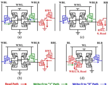
Fig. 6 shows the cell structures and corresponding paths of the read/write operation of published TFET SRAM cells [see Fig. 6(c) and (d)], the conventional 8T MOSFET SRAM cell [see Fig. 6(a)], and the 8T TFET SRAM cell [see Fig. 6(b)].
Fig. 6. Cell structures and corresponding read/write paths for the (a) conven-tional 8T MOSFET SRAM, (b) 8T TFET SRAM, (c) 7T TFET SRAM [9], and (d) 6T TFET SRAM [10].
Fig. 7. Comparisons of butterfly curves of the 8T MOSFET SRAM cell and the 7T/8T TFET SRAM cells in hold/read modes. The butterfly curve for the 6T TFET SRAM cell is also shown in Vdd = 0.6 V.
Read/Hold Modes: As shown, the 6T TFET SRAM cell
[see Fig. 6(d)] utilizes an inward access transistor for read and hence suffers from large read-disturb and shows worse RSNM (smaller than 50 mV at Vdd = 0.6 V). Both 7T and 8T TFET SRAM cells utilize the read buffer to decouple the read current path from the cell storage node to eliminate the read-disturb, except that the 7T TFET SRAM cell uses one transistor instead of two stacked transistors in the 8T TFET SRAM cell for read. Notice that one transistor read in the 7T TFET cell is possible due to the unidirectional current flow characteristics of the TFET that prohibits the current from the read transistors of unselected cells on the selected bitline from flowing into the bitline. (The forward-bias current is smaller than the reverse-bias current, as previously described in Fig. 4.) Fig. 7 compares the butterfly curves of the 8T MOSFET SRAM cell and the 7T/8T TFET SRAM cells in hold and read modes at Vdd = 0.6, 0.4, and 0.2 V, respectively. As shown, the transition of the voltage transfer characteristics (VTCs) of 7T/8T TFET SRAM cells is not as sharp as that of the 8T MOSFET SRAM cell. This is due to the delayed saturation characteristic and the broader crossover region in the TFET inverter discussed earlier, which degrades the H/RSNM. However, as Vdd scales down, this effect becomes less significant as the soft transition region in the TFET Id–Vgs characteristics is reduced, and the H/RSNM approaches that for the 8T MOSFET SRAM cell.
the 7T/8T TFET SRAM cells in write mode.
Fig. 9. (a) Write operation of the 8T TFET SRAM cell. (b) Corresponding write transient waveforms.
Write Mode: As shown in Fig. 6, all TFET SRAM cells use
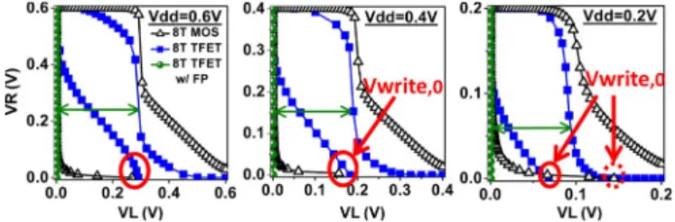
one transistor during the “write” operation, since the TFET transistor can only conduct current unidirectionally. As such, the WSNM of TFET SRAM cells is significantly worse than that of the 8T MOSFET SRAM cell (with the push–pull action during write), as shown in Fig. 8.
There are three major obstacles faced by the TFET 7T/8T SRAM cells during write. First, since the access transistor is faced outward (pull-down of the storage node), there is no “push” action; hence, no “disturb” in the write “1” VTC, resulting in degraded WSNM. Second, whereas the write “0” disturb is comparable among the 8T MOSFET SRAM cell and the 7T/8T TFET SRAM cells, due to the delayed saturation characteristic and the broader crossover region in the TFET inverter, the write “0” VTC of the 7T/8T TFET SRAM cells stay considerably higher than the write “0” VTC of the 8T MOSFET SRAM cells, thus further degrading the WSNM. Similar to the case for H/RSNM, this effect becomes less significant as Vdd scales down. Third, the use of only one (pull) transistor during the “write” operation and the broad crossover region between competing currents from the access n-type TFET and the holding p-type TFET cause a plateau in the low-going cell storage node voltage [see the dashed circle region in Fig. 9(b)], thus retarding the write-ability and write performance.
Write-Assist: In order to improve the write-ability and write
performance of TFET SRAM cells without adding cell tran-sistors (e.g., using the full transmission gate instead of the single pass transistor to improve the write operation), write-assist circuit techniques such as footed virtual ground [as that used by the 6T TFET SRAM cell in Fig. 6(d)] and floating-power (FP) line write [14] can be used. In Fig. 8, we show that the use of FP write-assist improves the WSNM significantly for the 7T/8T TFET SRAM cells.
DL TFET SRAM cell.
IV. 7T DL TFET SRAM
Based on the analysis in Section III, the use of an extra read-ing transistor to decouple the read current path from the storage node eliminates read-disturb and enhances the RSNM, whereas the unidirectional characteristics, the delayed saturation output characteristic, and the broad soft Id–Vgs transition region of the TFET device significantly reduce the WSNM. Thus, there is a need for a TFET SRAM cell with better write-ability and write performance.
A. Cell Structure of 7T DL TFET SRAM
Fig. 10 shows the proposed 7T DL TFET SRAM cell struc-ture and the corresponding read/write paths. The 4T DL FinFET SRAM cell introduced in the literature [15] exploits the capabil-ity of independent-gate control. The process and area overhead of independently controlled gate were reported/discussed in [16]–[19]. The main idea is to combine the access transistor and pull-down transistor into one independently controlled-gate pull-down device (NL/NR) with its back gate serving as the access transistor. The source node of NL/NR is connected to bitlines BL/BLB, which are predischarged to “low” state. We adopt the DL scheme and add two p-type TFETs as write access transistors on each side with their source nodes connected to BL/BLB. We now analyze the device characteristics of the tied-gate (DG-mode) and single-tied-gate (SG-mode) TFET devices.
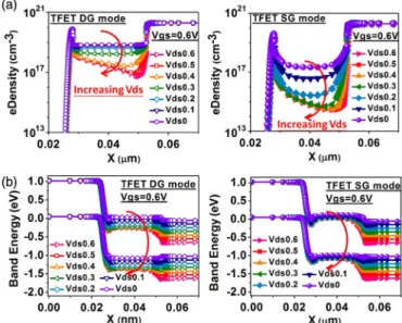
The differences of output characteristic between DG-mode and SG-mode of the TFET device are compared in Fig. 11(b) with the drain current of the individual device normalized to its maximum current at Vgs = Vds = 0.6 V, respectively, since the current in DG-mode is significantly higher than the current in SG-mode, it cannot be clearly distinguished with absolute drain current values. The arrows with tangential lines indicate the voltages where the maximum output conductance (gds) values occur, which can be regarded as the starting point
of the channel-resistance-limited region. Thus, for the TFET device operates in SG-mode, the delay saturation characteristic is not as severe as in DG-mode. The reason is explained in the following. As shown in Fig. 11(a), the effective VT (defined
by the constant-current method) of the TFET device in SG-mode is higher than that in DG-SG-mode for a given bias, since the electron carrier induced in the channel region is smaller. As Vds increases, the electron density of the TFET device decreases more rapidly in SG-mode than in DG-mode, as shown in Fig. 12(a). Thus, the TFET device in SG-mode enters the channel-resistance-limited region earlier than in DG-mode.
1096 IEEE TRANSACTIONS ON ELECTRON DEVICES, VOL. 60, NO. 3, MARCH 2013
Fig. 11. (a) Ids–Vgs characteristics at Vds = 0.6 V for the TFET device in DG-mode and SG-mode. The inset in (a) shows the TFET device in SG-mode operation. (b) Ids–Vds characteristic in DG-mode and SG-mode with the drain current normalized to the individual maximum current.
Fig. 12. (a) Electron density of the TFET device in DG-mode and SG-mode at Vgs = 0.6 V with different applied drain bias. (b) Band diagrams of the TFET device in DG-mode and SG-mode with different drain bias.
In Fig. 12(b), for SG-mode, at Vds = 0.2−0.25 V, the tun-neling width reaches its minimum, and a further increase of Vds appears across the depletion region of the drain side and can no longer influence the tunneling width. For DG-mode, the TFET device does not enter the channel-resistance-limited region until the drain bias increases to Vds = 0.4−0.5 V. Thus, for the TFET device operates in SG-mode, the output saturation characteristic is better than in DG-mode. For the proposed 7T DL TFET SRAM cell during hold and read modes, due to the better output characteristic of TFET device in SG-mode (data retained by the cross-coupled latch of DG-mode pMOS and SG-mode nMOS), the hold/read stability is improved. As shown in Fig. 13(a), at Vdd = 0.6 V, the H/RSNM of the proposed 7T DL TFET SRAM cell is 16% larger/better than the tied-gate (DG-mode) 8T TFET SRAM cell.
B. Operation Principles of 7T DL TFET SRAM
During write “0” operation, BLB, i.e., the source node of the NR, is charged “high,” thus facilitating the pull-up of the cell storage node QB [see Fig. 13(c)]. As such, Vwrite,1 becomes
Fig. 13. (a) H/RSNM of the 7T DL TFET SRAM cell. (b) WSNM of the 7T DL TFET SRAM cell. (c) Schematics of the write operation. (d) Write transient waveforms for the proposed 7T DL TFET SRAM cell and the 8T TFET SRAM cell.
very close to Vdd, as shown by the vertical straight line near Vdd (0.6 V) in Fig. 13(b), resulting in a significantly improved WSNM compared with the 8T TFET SRAM. The added p-type access TFET (pass “1” better than the n-type TFET) helps pull QB to “high” state, whereas NL pulls Q to “low” state, thus eliminating the plateau region for the low-going cell storage node QB and significantly improving the write performance compared with the 8T TFET SRAM [see Fig. 13(d)].
C. Comparisons of Stability and Performance of TFET SRAM Cells
We now compare the stability and performance of the 8T MOSFET SRAM cell, the 8T TFET SRAM cells with and with-out FP write-assist, and the proposed 7T DL TFET SRAM cell.
Stability: Fig. 14(a) compares the H/RSNM of the 8T
MOSFET SRAM cell, the 8T TFET SRAM cell and the 7T DL TFET SRAM cell. As shown, the proposed 7T DL TFET SRAM cell has a slightly better H/RSNM than the 8T TFET SRAM cell, and both approach that of the 8T MOSFET SRAM cell at Vdd = 0.2 V. Fig. 14(b) compares the WSNM of the 8T MOSFET SRAM cell, the 8T TFET SRAM cells with and without FP write-assist, and the proposed 7T DL TFET SRAM cell. The proposed 7T DL TFET SRAM cell is shown to offer the best WSNM among all cells.
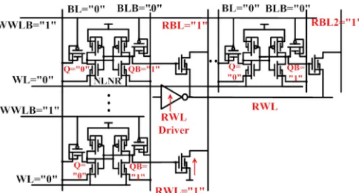
Performance: We consider an SRAM array with 32 cells per
wordline and 16 cells per bitline with a worst-case WL data pattern [where all the half-selected cells on the selected WL have QB = 1; thus, the WL driver has to sink the currents from all read bitlines (RBLs)] and the worst-case BL data pattern (where all the half-selected cells on the selected BL have QB = 1), as shown in Fig. 15. Fig. 16(a) shows the read
Fig. 14. Comparisons of stability of the 8T MOSFET SRAM cell, the 8T TFET SRAM cells with and without FP write-assist, and the proposed 7T DL TFET SRAM cell. (a) H/RSNM. (b) WSNM.
Fig. 15. SRAM array configuration with worst-case WL and BL data patterns.
Fig. 16. Comparisons of performance of the 8T MOSFET SRAM cell, the 8T TFET SRAM cells with and without FP write-assist, and the proposed 7T DL TFET SRAM cell in (a) read access time considering worst-case wordline and bitline data patterns and (b) time-to-write.
access time versus Vdd for the various cells considered. The read access time is defined as the time from when the input of the selected read wordline (RWL) driver reaches half-Vdd to when the RBL is pulled down to half-Vdd. As shown, the read performance of TFET SRAM cells outperforms MOSFET SRAM by about one and three orders at Vdd = 0.4 V and Vdd = 0.2 V, respectively. Fig. 16(b) compares the time-to-write, defined as the time from the 50% activation of the wordline to the time when the voltages of two cell storage nodes cross each other. The write performance of TFET SRAM cells is shown to also outperform MOSFET SRAM by about one and three orders at Vdd = 0.4 V and Vdd = 0.2 V, respectively. Furthermore, the proposed 7T DL TFET cell shows over a 30% write performance improvement compared with the 8T TFET SRAM using FP write-assist.
inverter. TFET SRAM cells with a single-type access transis-tor for write suffered from the lack of push–pull action due to TFET’s unidirectional conduction characteristics and large crossover contention from the holding transistor, resulting in insufficient WSNM and necessitating write-assist. A robust 7T DL TFET SRAM cell was proposed. The proposed 7T DL TFET SRAM cell, with better output characteristics in SG-mode, and decoupled read current path from cell storage node and push–pull write action with asymmetrical raised-cell-virtual-ground write-assist, provided a significant improvement in hold, read, and write stability and performance.
ACKNOWLEDGMENT
The authors would like to thank the National Center for High-Performance Computing in Taiwan for the software and facilities.
REFERENCES
[1] C. Aydin and A. Zaslavsky, “Lateral interband tunneling transistor in silicon-on-insulator,” Appl. Phys. Lett., vol. 84, no. 10, pp. 1780–1782, Mar. 2004.
[2] K. Boucart and A. M. Ionescu, “Double-gate tunnel FET with high-k gate dielectric,” IEEE Trans. Electron Devices, vol. 54, no. 7, pp. 1725–1733, Jul. 2007.
[3] A. Tura and J. Woo, “Performance comparison of silicon steep subthresh-old FETs,” IEEE Trans. Electron Devices, vol. 57, no. 6, pp. 1362–1368, Jun. 2010.
[4] F. Mayer, C. Le Royer, J.-F. Damlencourt, K. Romanjek, F. Andrieu, C. Tabone, B. Previtali, and S. Deleonibus, “Impact of SOI, Si1-xGexOI and GeOI substrates on CMOS compatible tunnel FET performance,” in
Proc. IEDM, 2008, pp. 1–5.
[5] R. Gandhi, Z. Chen, N. Singh, K. Banerjee, and S. Lee, “Vertical Si-nanowire-type tunneling FETs with low subthreshold swing (< 50 mV/ decade) at room temperature,” IEEE Electron Device Lett., vol. 32, no. 4, pp. 437–439, Apr. 2011.
[6] A. C. Ford, C. W. Yeung, S. Chuang, H. S. Kim, E. Plis, S. Krishna, C. Hu, and A. Javey, “Ultrathin body InAs tunneling field-effect transistors on Si substrates,” Appl. Phys. Lett., vol. 98, no. 11, pp. 113105-1–113105-3, Mar. 2011.
[7] S. H. Kim, H. Kam, C. Hu, and T.-J. K. Liu, “Germanium-source tunnel field effect transistors with record high ION/IOFF,” in VLSI Symp. Tech.
Dig., 2009, pp. 178–179.
[8] D. Kim, Y. Lee, J. Cai, I. Lauer, L. Chang, S. J. Koester, D. Sylvester, and D. Blaauw, “Low power circuit design based on heterojunction tunneling transistors (HETTs),” in Proc. Symp. Low Power Electron. Des., 2009, pp. 219–224.
[9] J. Singh, K. Ramakrishnan, S. Mookerjea, S. Datta, N. Vijaykrishnan, and D. Pradhan, “A novel Si-tunnel FET based SRAM design for ultra-low power 0.3 V VDD applications,” in Proc. ASP-DAC, 2010, pp. 181–186. [10] X. Yang and K. Mohanram, “Robust 6T Si tunneling transistor SRAM
design,” in Proc. Des. Autom. Test Eur., 2011, pp. 1–6.
[11] A. Mallik and A. Chattopadhyay, “Drain-dependence of tunnel field-effect transistor characteristics: The role of the channel,” IEEE Trans. Electron
Devices, vol. 58, no. 12, pp. 4250–4257, Dec. 2011.
[12] Sentaurus User’s Manual, Synopsys, Mountain View, CA, 2011. [13] L. Chang, D. M. Fried, J. Hergenrother, J. W. Sleight, R. H. Dennard,
R. K. Montoye, L. Sekaric, S. J. McNab, A. W. Topol, C. D. Adams, K. W. Guarini, and W. Haensch, “Stable SRAM cell design fort the 32 nm node and beyond,” in VLSI Symp. Tech. Dig., 2005, pp. 128–129.
1098 IEEE TRANSACTIONS ON ELECTRON DEVICES, VOL. 60, NO. 3, MARCH 2013
[14] M. Yamaoka, N. Maeda, Y. Shinozaki, Y. Shimazaki, K. Nii, S. Shimada, K. Yanagisawa, and T. Kawahara, “Low-power embedded SRAM mod-ules with expanded margins for writing,” in Proc. ISSCC Dig. Tech.
Papers, Feb. 2005, pp. 480–481.
[15] B. Giraud, A. Amara, and A. Vladimirescu, “A comparative study of 6T and 4T SRAM cells in double-gate CMOS with statistical variation,” in
Proc. Int. Conf. Circuits Syst., 2007, pp. 3022–3025.
[16] W. Liu, K. Etessam-Yazdani, R. Hussin, and M. Asheghi, “Modeling and data for thermal conductivity of ultrathin single-crystal SOI layers at high temperature,” IEEE Trans. Electron Devices, vol. 53, no. 8, pp. 1868– 1876, Aug. 2006.
[17] S. Natarajan, M. Armstrong, M. Bost, R. Brain, M. Brazier, C.-H. Chang, V. Chikarmane, M. Childs, H. Deshpande, K. Dev, G. Ding, T. Ghani, O. Golonzka, W. Han, J. He, R. Heussner, R. James, I. Jin, C. Kenyon, S. Klopcic, S.-H. Lee, M. Liu, S. Lodha, B. McFadden, A. Murthy, L. Neiberg, J. Neirynck, P. Packan, S. Pae, C. Parker, C. Pelto, L. Pipes, J. Sebastian, J. Seiple, B. Sell, S. Sivakumar, B. Song, K. Tone, T. Troeger, C. Weber, M. Yang, A. Yeoh, and K. Zhang, “A 32 nm logic technology featuring 2nd-generation high-k + metal-gate transistors, enhanced chan-nel stain and 0.171 μm2 SRAM cell size in a 291 Mb array,” in Proc.
IEDM, 2008, pp. 1–3.
[18] R. V. Joshi, K. Kim, R. Q. Williams, E. J. Nowak, and C.-T. Chuang, “A high-performance, low leakage, and stable SRAM row-based back-gate biasing scheme in FinFET technology,” in VLSI Symp. Tech. Dig., Jan. 6–10, 2007, pp. 665–672.
[19] K. Endo, S.-I. O’uchi, Y. Ishikawa, L. Yongxum, T. Matsukawa, M. Masahara, K. Sakamoto, J. Tsukada, K. Ishii, H. Yamauchi, and E. Suzuki, “Enhancing noise margins of FinFET SRAM by integrating Vth-controllable flexible-pass-gates,” in Proc. Eur. Solid-State Device
Res. Conf., 2008, pp. 146–149.
Yin-Nien Chen received the B.S. degree from Na-tional Tsing Hua University, Hsinchu, Taiwan, in 2009. She is currently working toward the Ph.D. degree at National Chiao Tung University, Hsinchu.
Ming-Long Fan (S’09) received the B.S. and M.S. degrees from National Chiao Tung University, Hsinchu, Taiwan, where he is currently working to-ward the Ph.D. degree in the Institute of Electronics.
Vita Pi-Ho Hu (S’09–M’13) received the Ph.D. de-gree from National Chiao Tung University, Hsinchu, Taiwan, in 2011.
She is currently an Assistant Researcher with Na-tional Chiao Tung University.
Pin Su (S’98–M’02) received the Ph.D. degree from the University of California, Berkeley, CA, USA.
He is currently a Professor with the Department of Electronics Engineering, National Chiao Tung University, Hsinchu, Taiwan.
Ching-Te Chuang (S’78–M’82–SM’91–F’94) re-ceived the Ph.D. degree from the University of California, Berkeley, CA, USA, in 1982.
Since February 2008, he has been a Chair Profes-sor with the Department of Electronics Engineering, National Chiao Tung University, Hsinchu, Taiwan.