Optical properties of inorganic AgSb recording thin film
Y. H. Fang, P. C. Kuo,a兲and P. W. Chen
Institute of Materials Science and Engineering, National Taiwan University, Taipei 106, Taiwan Wei-Chih Hsu
Photovoltaics Technology Center, Industrial Technology Research Institute, Hsinchu 310, Taiwan C. Y. Chou and T. H. Wu
Institute of Materials Science and Engineering, National Taiwan University, Taipei 106, Taiwan 共Received 3 March 2006; accepted 27 May 2006; published online 30 June 2006兲
50 nm Ag1−xSbx共x=10.8–25.5兲 thin films were prepared by magnetron sputtering. Thermal analysis shows that the phase change occurs around 250 ° C. The optical property analysis show that the as-deposited Ag80.9Sb19.1 films have high reflectivity of about 62%–73%. After heat treatment at 300 ° C, the contrast of Ag80.9Sb19.1film is 12.5%–17% for wavelengths between 400 and 800 nm. Dynamic test shows that using the Ag80.9Sb19.1film as the memory layer of write once optical disk, a carrier-to-noise ratio of about 45 dB can be achieved at =657 nm, numerical aperture of 0.65, and a linear velocity of 3.5 m / s. © 2006 American Institute of Physics.关DOI:10.1063/1.2218774兴
As present, the recording layer of write once and read many 共WORM兲 optical disk is usually made of organic dyes.1,2Since the wavelength range that can be absorbed by organic dyes is narrow, absorption by organic materials can-not fulfill the requirements of high density optical memory.3 Again, it is not easy to get a uniform layer of the organic dye in the high density recording disk. Recently, inorganic mate-rials were investigated to replace organic dyes in blue ray disks and digital versatile disks共DVDs兲.
In 1993, Baba et al.4,5studied the possibility of applying an inorganic metal thin film including Au, Ag, Cu, and Al to WORM optical disks. When the thickness of the metal film is thinner than 10 nm, the as-deposited film is formed of nanoclusters. It would have high reflectivity and absorption. Since only the nanostructure of the metal thin film is changed when the metal film absorbs laser energy, it would not take long time in writing. They found that Ag-based metal thin film has high reflectivity and high reflectivity change. On the other hand, it has been known that Sb has high crystallization rate.6We expect that the combination of Ag and Sb may have high reflectivity and high crystallization rate. In this work, we used a Ag-based material in the form of Ag1−xSbxfilms, measured its optical properties, and investi-gated the possibilities of applying it to the WORM disk.
For analysis of the optical properties, a ZnS – SiO2 pro-tecting layer with a thickness of 1000 Å was deposited by radio frequency共rf兲 magnetron sputtering on naturally oxi-dized Si 共100兲 wafer and Marienfeld cover glass. The Ag1−xSbxrecording films共x=10–26 at. %兲 with thickness of 1000 Å were deposited on ZnS – SiO2on the protecting layer by rf cosputtering of Ag and Sb targets. For dynamic tests, a Ag 共1000 Å兲 reflecting layer was further deposited on the Ag1−xSbxlayer by rf magnetron sputtering with an Ar pres-sure of 3 mTorr. After deposition, the films were annealed at various temperatures in vacuum for 5.5 min and then quenched in ice water. The crystal structures of the films were investigated by x-ray diffraction 共XRD兲 with Cu K␣ radiation and field emission gun transmission electron
mi-croscopy 共FEG-TEM兲. Composition of the film was deter-mined from the energy dispersive spectrum 共EDS兲. The thickness of the film was measured by ␣ step and atomic force microscope 共AFM兲. Dynamic tests of disks were car-ried on a Pulstec DDU-1000 machine.
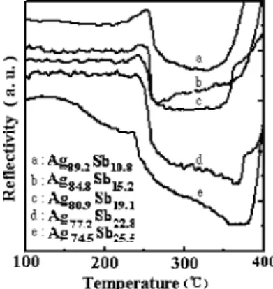
Figure 1 shows the relationship between reflectivity and temperature of the as-deposited Ag1−xSbx films at a heating rate of 50 ° C / min. Two reflectivity changes are clearly ob-served in all the films as the temperature is increased from 100 to 400 ° C. It indicates that the first phase transition tem-perature of Ag1−xSbx films is around 250 ° C. Moreover, a higher reflectivity is observed when the Sb content of the film is lower than 19.1 at. %. But the films with Sb content lower than 19.1 at. % have lower contrast around 250 ° C than that of Sb content higher than 19.1 at. %. However, only the reflectivity of Ag80.9Sb19.1film is stable lower and higher the phase transition temperature. Therefore, the Ag80.9Sb19.1 film will be examined in detail.
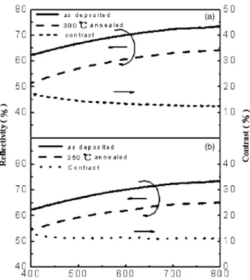
Figures 2共a兲 and 2共b兲 show the reflectivity and contrast of the as-deposited and annealed Ag80.9Sb19.1films at various laser beam wavelengths, and annealing temperatures of 300 and 350 ° C, respectively. The reflectivity of the Ag80.9Sb19.1 film is decreased after annealing at 300 or 350 ° C. From the x-ray diffraction pattern 共Fig. 3兲, we observed that the as-deposited Ag80.9Sb19.1 film has an orthorhombic
⬘
-AgSba兲Author to whom correspondence should be addressed; FAX: ⫹886-2-23634562; electronic mail: [email protected]
FIG. 1. Variation of reflectivity with temperature of the as-deposited Ag1−xSbxfilms.
APPLIED PHYSICS LETTERS 88, 261917共2006兲
0003-6951/2006/88共26兲/261917/3/$23.00 88, 261917-1 © 2006 American Institute of Physics
crystalline structure. The orthorhombic structure is the cause of the optical anisotropy. By grain refining, the optical aniso-tropy could be reduced to avoid the difference of reflection from different grain orientations.7Figures 4共a兲–4共c兲 show the TEM images and electron diffraction patterns of the as-deposited, annealed at 300 and 350 ° C Ag80.9Sb19.1 films, respectively. From Fig. 4共a兲, it is found that the grain sizes are about 5 – 10 nm and the grains are uniform for the as-deposited film. The optical anisotropy is reduced due to this small and uniform grain size which leads to the large reflec-tivity of the as-deposited Ag80.9Sb19.1film, as shown in Figs. 2共a兲 and 2共b兲. After the Ag80.9Sb19.1films are annealed at 300 or 350 ° C, the grain sizes grow to 10– 100 nm. These non-uniform grain sizes would cause more optical anisotropy and lead to a reduction in the reflectivity of the film. Therefore, the reflectivity of the Ag80.9Sb19.1film after annealing at 300 or 350 ° C would be lower than the as-deposited film, as
shown in Figs. 2共a兲 and 2共b兲. The contrasts of the Ag80.9Sb19.1 films are about 12.5%–17% and 11%–12% in the wavelength between 400 and 800 nm for the films an-nealed at 300 and 350 ° C, respectively.
Since the Ag80.9Sb19.1film has higher reflectivity, higher optical contrast, and suitable phase transition temperature, we take the Ag80.9Sb19.1disk for dynamic tests. The dynamic test was conducted at=657 nm, numerical aperture 共NA兲 = 0.65, and DVD 1X and 14T. Figure 5 shows the relation-ship between the writing power and carrier-to-noise ratio 共CNR兲. The critical writing power is about 3 mW. A small recording area is formed when the writing power is smaller FIG. 2. Relationship among reflectivity, contrast, and laser beam
wave-length of the as-deposited,共a兲 300 and 共b兲 350 °C annealed Ag80.9Sb19.1 films.
FIG. 3. X-ray diffraction patterns of various as-deposited Ag1−xSbxfilms.
FIG. 4. TEM bright field image and diffraction pattern of the 共a兲 as-deposited,共b兲 300 and 共c兲 350 °C annealed Ag80.9Sb19.1films.
FIG. 5. Relationship between the writing power and carrier-to-noise ratio 共CNR兲 of the Ag80.9Sb19.1film.
261917-2 Y. H. Fang and P. C. Kuo Appl. Phys. Lett. 88, 261917共2006兲
than 4 mW. This leads to small CNR values 共less than 10 dB兲. If the writing power is in the range of 6–12 mW, the CNR values are higher than 45 dB due to larger recording area. This is quite satisfactory for the requirements of the WORM optical disk. The reason why the CNR value de-creases as the writing power is higher than 12 mW may be due to the distortion of the film structure of the disk at higher writing power. The distortion of film structure of the disk will increase the noise thus leading to a decrease in the CNR value.
To summarize, it is found that the as-deposited Ag80.9Sb19.1 film is well crystallized with a grain size of about 5 – 10 nm, so that it has a large reflectivity value共about 62%–73%兲. Moreover, the Ag80.9Sb19.1 film possesses large optical contrast within the laser beam wavelength range of 400– 800 nm and a large CNR value 共about 45 dB兲. This
film is a promising material for WORM disk.
This work was supported by the National Science Coun-cil and Ministry of Economic Affairs of Taiwan through the NSC 94-2216-E-002-009 and 94-EC-17-A-08-S1-0006 grants, respectively.
1J. J. M. Ruigrok, R. Coehoorn, S. R. Cumpson, and H. W. Kesteren, J. Appl. Phys. 87, 5398共2000兲.
2S. Miyanishi, K. Kojima, J. Sato, A. Takahashi, and K. Ohta, J. Appl. Phys. 93, 7801共2003兲.
3T. Minemura, H. Andoh, and Y. Maeda, J. Appl. Phys. 63, 4632共1989兲. 4K. Baba, K. Hayashi, and M. Miyagi, Electron. Lett. 29, 1948共1993兲. 5K. Baba, K. Hayashi, and M. Miyagi, Proc. SPIE 2338, 175共1994兲. 6K. Baba, Y. Ohkuma, T. Yonezawa, and M. Miyagi, Appl. Opt. 40, 2796
共2001兲.
7K. A. Rubin, Mater. Res. Soc. Symp. Proc. 230, 239共1992兲.
261917-3 Y. H. Fang and P. C. Kuo Appl. Phys. Lett. 88, 261917共2006兲