A
CMOS 5-GHz Micro-Power LNA
Hsieh-Hung Hsieh and Liang-Hung
Lu
Department of Electrical Engineering and Graduate Institute of Electronics Engineering,
National Taiwan University, Taipei, Taiwan, R.O.C.
Abstract
-
A fully integrated LNA suitable for ultra-low- voltage and ultra-low-power applications is designed and fabricated in a standard 0.18-pm CMOS technology. With complementary current-reused gain stages, the proposed amplifier exhibits 9.2-dB small-signal gain and 4,s-dB noise figure at 5 CHz while consuming 900-pW dc power from an extremely low supply voltage of 0.6 V. A gain/power quotient, which is widely used as the figure of merit for low-power amplifiers, o f 10.2 d B h W i s achieved in this work.I n d w Terms
-
CMOS RF, low-noise amplifiers, current reuse, ultra-low-power, ul tra-low-voltage.1.lNTRODUCTION
The increasing demands on portable wireless devices have motivated the development of low-power
RF
frontends. With recent advances in the high-frequency characteristics, CMOS has become the choice of technology due to its lower cost and higher level of integration. One major drawback of using CMOS at radio frequencies is the inherently low transconductance of the transistors. To achieve sufficient transconductance for R F applications, typical CMOS frontend designs involve high bias current and high power consumption, which reduces the battery lifetime of the portable devices. Besides, the supply voltage is also an important design issue in the implementation of CMOS RF circuits. As the feature size of the MOSFETs continues to shrink, the supply voltage is scaled down accordingly. Unfortunately, the performance of most RF circuits degrades significantly as the supply voltage decreases below 1V. In
order to take the advantage of advanced CMOS technologies, it is desirable to develop low-voltage techniques forW
frontend circuits with satisfactory performance.Being a crucial part in a frontend receiver, the low- noise amplifier (LNA) is recognized as one of the most power-consuming components. Recently, current-reused LNA topology [ 1 ] was reported to achieve high gain with minimum power consumption. However, the use of stacked NMOS stages limits its application in low-voltage designs. In order to reduce the required supply voltage, a folded cascode LNA was proposed [2]. Though the minimum supply voltage can be reduced by one transistor overdrive, the bias currents of the gain stages have to
be
0-7803-8983-2/05/$20.00 Q 2005 IEEE
r-7
f
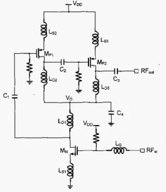
Fig. 1. Schematic of the micro-power LNA.
provided separately, resulting in an increase in power consumption. In this paper, a novel current-reused topology is proposed for the complementary cascaded amplifier. An ultra-low-power and ultra-low-voltage LNA is presented in a 0.18-pm CMOS technology for 5-GHz wireless applications.
Section I1 presents the circuit topology and design issues including bias scheme, small-signal characteristics, noise figure and linearity. The experimental results of the fabricated LNA are shown in Section 111. Finally, Section IV concludes this paper.
11. CIRCUlT DESIGN AND ANALYSIS A. LNA Topology
The proposed 0.6-V micro-power LNA with all on-chip components is shown in Fig. 1 . In order to provide high
LNA gain with a reduced supply voltage and minimum
31
power dissipation, cascaded gain stages are used in this design. The common-source MOSFETs, M,, M,, and M,, represent the first, second and third stage, respectively. By connecting the drain inductances of the gain stages together with an ac ground provided by the capacitor
C,,
the current-reused topology is established. Instead of stacking NMOS transistors to share the bias current in a conventional current-reused topology, complementary gain stages are used to further reduce the supply voltageby
one transistor overdrive. The stacking complementary stages are biased with the gate of M, connected to V,, and the gate of Mpl and M, tied to the ground through resistors.In a cascaded amplifier, it is required that all MOSFETs are saturated to provide sufficient signal amplification. Based on the dc analysis, the supply voltage, V,,, should be kept approximately between V, and 2Vt,,
where
V,,is
the threshold voltage of the MOSFETs. With a supply voltage higher than 2V,,, the transistors are driven out of saturation, resulting in a decrease of power gain. On the other hand, a supply voltage below V, turns off the transistors. Therefore, optimized LNA performance is achieved with a supply voltage of 0.6 V in this design.Once the supply voltage is determined, the voltage V, in Fig. 1 is designed to be half of V,, by the aspect ratios of the NMOS and the PMOS transistors. Note that the voltage V, is considered a quasi-stable dc operating point when both NMOS and PMOS are saturated. Typically, common-mode feedback (CMFB) is required to provide a stable dc bias at the output. In this design, capacitive coupling is used between the gain stages, and the MOSFETs are biased at the verge of the saturation region due to the reduced
supply
voltage. Therefore, the middle point voltage V, has better tolerance with respect to the process and supply voltage variation. Good bias stability is achieved by properly choosing the design parameters without CMFB.B. Small-Signal Characteristics
The LNA design is originated from a three-stage cascaded amplifier. Taking the carrier mobility and the device parasitics into consideration, NMOS is used as the input stage, followed by two
PMOS
stagesin
common- source configuration. Inductive source degeneration technique (L, and Ls,) is adopted for the input matching while the output matching is provided by C, and LD3. In addition, LC networks (C,, L,,) and (C2,LD2)
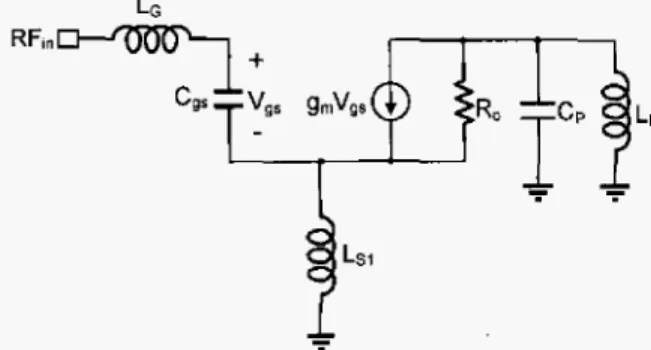
in between the gain stages are used as the inter-stage matching and dc block.The simplified small-signal equivalent circuit for the input stage is shown in Fig. 2, where L, and
C,
are the shunt reactive elements at the drain of M,. If the value ofL G
Fig. 2. The small-signal equivalent circuit of the input stage.
C , is 'sufficiently
large,
the , shunt inductance L, isapproximated by L,,, while C, represents the series connected of C, and the input capacitance of the second stage. In this design, L, is chosen to resonate with C , at the frequency of interest. With the parallel resonance at the drain terminal, the gain of the input stage is enhanced regardless of the input capacitance of the second stage. As
a result, the overall noise figure of the LNA is reduced due to the suppression of the noise contribution from the following stages.
C. Noise and Linearity
In addition to the small-signal gain, the noise figure and the linearity are the most important circuit parameters in a
LNA design, especially for ultra-low-power and ultra-
low-voltage applications, Due to the similarity in circuit topology, the analysis of the proposed LNA is simplified as a three-stage cascaded amplifier.
In a typical three-stage cascaded amplifier, the overall noise figure can be obtained by the equation [3] as
where NFi and Ap, represent the noise figure and the available power gain of the i-th stage, respectively. Therefore, it
is
desirable to have a minimumNF,
while maintaining Ap, sufficiently large to suppress the noise contributions from the following stages. Since the transistors are biased at low bias current and overdrive voltage in the proposed topology to achieve micro-power operation, a degradation in the noise figure is expected as suggested in [4]. In addition, the noise contributed from the following stages can not be neglected due to the moderate gain of the first stage. The LNA design involvesthe trade-offs between the gain and the noise figure of the individual stages 'to optimize the overall amplifier gain with an acceptable noise figure.
Fig. 3. The micrograph of the fabricated LNA.
In a cascaded amplifier, the linearity parameters, such as the input-referred 1 -dB gain compression point (Pln-,dB) and the input third-order intercept point (TIP,), are dominated by the last gain stage. Typically, better amplifier linearity can be obtained by increasing the transistor size and the bias current of the output stage. For
the proposed LNA topology, the bias current of the output stage is limited to achieve the minimum power dissipation. Therefore, a fundamental restriction is imposed on the Pin.
,dD and IIP, in the implementation of a micro-power LNA.
111. EXPERIMENTAL RESULTS
The proposed LNA was designed and fabricated in a standard 0.18-ptn CMOS technology. Figure 3 shows the micrograph of the fabricated LNA with a chip area of 0 . 8 6 ~ 1 .l mm2 including the pad frame. On-wafer probing
was performed to characterize the circuit performance of the LNA.
The measured small-signal characteristics of the micro- power LNA are illustrated in Fig. 4. The LNA consumes a dc power of 900 FW from an ultra-low supply voltage of 0.6 V. Due to the use of the cascaded gain stages and the inter-stage resonance, a small-signal 'gain of 9.2 dB is achieved at the center frequency
of
5 GHz. With on-chip matching networks, the input and output are matched to 50 around its center frequency. The measured SI, and S, are -12 dB and -20.9 dB, respectively. In addition to thesmall-signal characteristics, noise figure measurement was performed without external noise matching. As can be 10
5
9 5 e!s
o
.-
41
2
-5 0 - 1 0 3 m 0 e m C m .- -1 5 c t - - 4 4.5 5 5.5 6 Frequency (GHz) 15 5 -d
me
F
-5 m v) 7 c -1 5 -25Fig. 4. The measured small-signal performance of the LNA.
/ 0 - I O -
- -
h E -20 a ---8
-301
a -40 -8
-50 -2
-60 ~ -35 -30 -25 -20-15
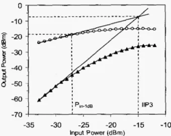
-10 Input Power (dBm)Fig. 5. The measured P,n.lm and IIP, of the LNA with input frequency spacing of IO MHz.
seen from Fig. 4, the LNA exhibits a noise figure of 4.5 dB at 5 GHz.
For the evaluation of the large-signal behavior, the
IIP,
and the Pin.,dB
of
the LNA were obtained by two-tone harmonic measurement with 10-MHz input frequency spacing. The measured Pin.,d8 and IIP, are-27 and
-15dBm, respectively, as shown in Fig. 5 . The linearity of the LNA is mainly limited by the power dissipation of the third stage. In this work, the micro-power LNA is designed for optimized gain at the cost of noise figure and linearity.
Pm-ldB
11P3 GainlPd,
The performance of the micro-power LNA is summarized in Table I together with the results from previously published data [5]-[7] for comparison. The
proposed LNA has the lowest power consumption and supply voltage while maintaining a satisfactory gain and noise figure at 5 GHz.
A
gaidpower quotient of 10.2 dB/mW is achieved in this design. It is suitable forultra-
low-voltage and ultra-low-power wireless applications.
dBm -27 3.7 -1 5.8 -14.0 d Bm -1 5 -7.25 - ~ ~ - dBlmW 10.2 1.44 5.33 9.01 0.59 IV. CONCLUSION
A micro-power LNA using a standard 0.18-pm CMOS technology is presented. By employing current-reused
topology and inter-stage resonance technique, the fully integrated
LNA
exhibits a 9.2-dB power gain and 4.5-dl3 noise figure at 5 GHz while consuming 900-pW dc power from an ultra-low supply voltage of 0.6V.ACKNOWLEDGEMENT
This work was supported in part by the National Science Council under Grant No. 93-2220-E-002-003 and 93-2220-E-002-009. The authors would like to thank National Chip Implementation Center (CIC) for chip fabrication and technical supports.
REFERENCES
Triquint Semiconductor, ‘TQ9203, low-current RF IC downconvertor,” in Wireless Communication Products,
1995.
Eyad Abou-Allam and Tajinder Manku, “A low voltage design technique for low noise RF integrated circuits,”
ISCAS 1998, vol. 4, pp. 373-377, June 1998.
Guiilenno Gonzalez, Microwave Transistor Amplifiers: Analysis and Design, Prentice Hall, 1997.
Derek K. Sfiaeffer and Thomas H. Lee, “A 1 S - V , 1.5-GHz
CMOS low noise amplifier,” IEEE J. Solid-State
Circuirs, vol. 32, no. 5 , pp. 745-759, May 1997.
Kousuke Ohsato and Toshihiko Yoshimasu, “lnternally matched, ultralow dc power consumption CMOS amplifierfor L-band personal communications,” IEEE
Microwave and Wireless Components Letters, vol. 14, no. 5, pp.204-206, May 2004.
D.
Linten, et al., “Low-power 5 GHz LNA and VCO in 90 nm RF CMOS,” V U 1 Circuits Symposium 2004, pp. 372 -375, June 2004.
M.
N.
El-Gama], K. H. Lee and T. K. Tsang, “Very low- voltage (0.8V) CMOS receiver frontend for 5GHz RF applications”, Circuits, Devices and Sysferns, IEEProceedings, vol. 149, 110.516, pp.355