A
FREQUENCY ESTIMATION ALGORITHM FOR
ADPLL
DESIGNS
WITH
TWO-CYCLE LOCK-IN
TIME
Chia-Tsun Wu, Wei Wang, I-Chyn Wey, An-Yeu (Andy) Wu
Graduate Institute of Electronics Engineering, and Department of ElectricalEngineering, National Taiwan University, Taipei 106, Taiwan, R.O.C.
Abstract-This paper presents a Frequency-Estimation This paper presents a Frequency-Estimation Algorithm Algorithm for the ADPLL designs instead of traditional (FEA) for frequency-acquisition in two-cycle lock-in time, binary frequency-search algorithm. With the proposed with stable output frequency. We proposed a close-form ADPLL architecture and synchronization process, the lock analysis in time domain than others approach. A new VLSI time can be optimized to two cycles. As the reference clock architecture of ADPLL is also developed and realized in varies or frequency multiplication switches, lock time holds UMC 0.18
lp6m
CMOS process. Cooperated withintwo reference clock cycles. An implementation of proposed proposed scalable digital lock detector, the proposed ADPLL design is realized in UMC 0.18 pm 1P6M CMOS ADPLL is suitable to fit demands of different design technology with core area of 520x530 pm2. The PLL has the applications.
frequency range of 140 MHz to 1030 MHz with 22ps DCO resolution.
Reference Clock
1. INTRODUCTION frePFD LoopFilter
PLL (Phase-Locked Loop) is widely used for various
applications, especially in wire/wireless communications,
FrequencF
oDigitallyOControlled)
CDR (Clock Data Recovery), and clock generators. In
FaOutput
Clocllfo
recent years, SoC (System-on-Chip) becomes a major Figure 1 AtypicalADPLLblockdiagramwith
trend. The ADPLL (All-Digital Phase-Locked
Loop)
r.
frequency-applies digital design methodology to avoid mixed-signal design problems, and is suitable to be packed as hard IP,
firm IP, and soft IP. These advantages make ADPLL very II.PROPOSEDFREQUENCY-ESTIMATIONALGORITHM attractive to beintegratedinto SoCdesigns. The main feature ofFEA is based on
1)
CorrelationsAnother ADPLL advantage is that the ADPLL usually between reference clock and DCO characteristics; 2) employs frequency-searching algorithm to achieve high- Analysis of DCO control code in time domain. The desired performance frequency lock-in time [1][2][4] as shown in frequency output
f,
canbe obtained by further calculation Fig. 1. This fast-locking ADPLL is very useful for instead of traditional search.frequency hopping based FHSS (Frequency-Hopping In this context,
frf
andf
represent thefrequencies
of Spread Spectrum) applications such as 802.11, BluetoothInticoex,read epsnthefqucesfSpeandFHMAe (FrequenaicyHoping Multiple802.1
,Access)to%
referenceclock,
and desiredoutput
frequency,
respectively.
UWBFHMA
(UltraeWideBand)
ince
Multh
ple
Acinss) af
N ismultiplication
factor. Thefrequency
multiplication
UW
(lta
idetransceiver ifunction
ofa PLLinlockedstateisdescribed
asFHSS/FHMA system switches carrier frequencyrapidly, a fast-switching and stable frequency synthesizerto generate
thehopping carrier frequency is essential to FHSS/FHMA fo Nxfre1 (1)
transmitters and receivers.
Parameters aredefined for clarification:
MostanalogPLLs provide higher frequency resolution,
-ref
The cycle time of reference clock.but suffer from slow acquisition time. Lots of ADPLLs
Tmi,
The minimumcycle
time of DCO when DCO employ Binary Search Algorithm (BSA) as frequency- operatesatthe maximumoscillating frequency
search algorithm torour 1 * *achieve faster lock-in time. The BSA1 1 r 11 *1 rT^1 1 R
RmansThe maximum
The maximumcycletime ratio
oscillatin fequen cy
between reference[2][4]
is a very simple, and useful algorithm. The search clock and DCO clock.(DCO
operated
atTmi,)
complexityis 0(log2n). Using* r 1 1 1the BSArT^1 1 1 * *canreduce lock-in T;~maxc The maximum cycle time of DCO when DCOclc
andmDC
clo
(DCOopaD
at DCOtime to 16 reference clock
cycles [3].
The lock-in time can operatesattheminimum
oscillating
frequency. beimproved
more than 40 times faster than traditional R Tcanalog PLL [5]. Another approach for frequency-search
uses TDC (Time-to-Digital Conversion), and developed clock and DCO clock. (DCO operated at 'max) DCO~~~~~~~arhtetr [1oaheesvnccelc-ntm. Then, the correlations between reference clock and DCO
lock-in
range are deducedasRmin Tmax =Rma Tmin =ref (2) feature of proposed FEA is, even under temperature
Rm*n'ma
-RaxmJ
rref2 fluctuations, power supply or process variations, the FEATransformations from (2) givesexactlythe desired control code.
Assume an ADPLL operatesfrom 100MHz to 500MHz
_Tref
- ref with 14 bits binary control code of DCO. The behaviorTmax
Rmm
TmiM-
Rmax
simulations of proposed algorithm and BSA are shown (3) within Fig. 2. When the BSA is applied in the frequency Consider a DCO provides Tfrequency acquisition steps. acquisition, the step size will be divided by two after for Then, we can derive the relation between resolution and each frequency-search. Output frequency is unstable during difference of andzmin
as convergence process in Fig. 2(a). The proposed FEA locks the reference clock in very fewcycles
with a stableTref
~ convergence process asshown inFig.
2(b).
Tref ref
Ar - Tmax
-min
Rmin
Rmax
400T T
(4)
350
J
B00~300 '0
whereJXis the DCOacquisitionresolution, and Tis the
total number of DCOacquisitionsteps. 100
200
After ADPLL closedloop converges, the cycle time of * 10o 0 0
~~~~~~~~~~~0 10 fr °f30B s40 50 ( a 0 10 t?OefC1SlS 40 50(b
outputfrequencycanbedescribedas eV
(b)
1 Figure 2. (a)Behavior simulation ofbinary-searchalgorithm. (b)
=FxAr+ m Improved convergence of
frequency-estimation
algorithm.(5)
whereFis the desired controlcode foraccurate
frequency.
III. PROPOSED ADPLL ARCHITECTUREFORTWO-CYCLE
LOCKING
From(1),and(5) The VLSI architecture, Fast-Lock Engine (FLE), is
developed to realize FEA algorithm in Fig. 3(a). With Nx
(F
xA T+Tmin)Tref
(6) cooperation of FLE, an ADPLL design can providefast-lockoperation. Equation(6)denotes therelationshipbetween reference
clock and DCO parameters after closedloopconverges.
F--
--L-ck
EngineFrom
(3), (4),
and(6)
wehave (a) InnerDCOHoperatedatFa Inner DCOLoperatedatF.Iefreref
C Cycle CounterR, CycleCounterRminref ref.1
Lock Fast
Frequency-kXF
Rin Rmax lefr = T-J ONx!FxR 7 +; J0rf 7 ()
'rref
Detector Estimation~~~~~~~~~~~~~~System
& DCOController
PFD LoopFilter
Afterreorganization,the desired DCO control codeFis
expressedas FeedbackClock FrequencyDivider Output Cock,fo OutputDCO
(T x
Rmax
XRmin)
-(TxRmin
xN)TyjicADRL
LoF-
NX(R
-R)
Figure3. ProposedADPLLarchitecture fortwocycles lock.NX max
-kin)J(8
When targeting at frequency acquisitionwith two-cycle
Note that theTmax, Tmin, andJS areparameters of process
lock-n
time,inx
an
rmun
shou
beconcu
edependence,
and difficult to be identified beforeavai
Hene,
twoaddioain
DCOs are uilized in fabrication. Also, the exact value ofi+ef
varies betweenproposed
ADPLLconfigtion.
innerDCOH
and
udCO
applictions
Bu.m
n mncnb bandbproposed
ADPLLconfiguration.
Inner DCOH and DCOLapplicaions.
But Rmax and Rmin can be obtained by were operated at the highest / slowest frequencyfrequency counters and dividers during run time. Also, the g q
y,'
TiSone ofpre-defined parameters of theDCO, and NiSthe repcilyThgnradcoksgasaetasmtd mutpicto fatr Bae oncreae
'eedny
separately to cycle-counters.While
system controller * . '~~~~~~~~receives
Rmax, and Rmin from two cycle-counters, the F can can b calulatdbypropsed FA (8. Animpotant be calculated fordesired
frequencyaccording
to FEA.A. Fast-Lock Process
fd1vF
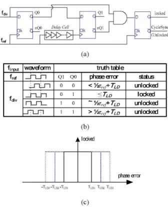
ll~ QO QI lockedFig. 4(a)
illustratessynchronization
between reference lD D DD cclock,
andfo.
Assumeafrequency
step isapplied
tothefref
-nQO DelayCell oQI CycleSyncat cycle
1
inFig. 4(b). The LD(Lock Detector)detects the > (Unlocked)frequency step during cycle I and activates trigger-signal frd II
(CycleSync). The Rmax and Rmin are both calculated
(a)
simultaneously. TheDFFsuspends DCO on therising edge
ofcycle 2 andFLE is now activated. FLE calculates theF
finput
waveorm truthtableduring cycle
2. Atlast,
the DCO resumeswithnew control fref JLF Qi QO phaeerror stauscodeFattherising edge of cycle 3. Based on this process, 22r-1 0 0 <
1/2Trejt
TLD unlocked fast-lock frequency acquisition can be realized in two f 0 1<cTLD
d(edcycles.
div
-- 1 0Y/2rei
TLD unlockedFast-lock Normal _ 1 1 >Y/2reI TLD unlocked
ControlCode,F Control Code
T D (b)
fref |,dk rL T Digitally-Controlled
ocked
rdear Oscillator
-CycleSync ( .ha.,[
.phaseerror
- Cycle 1I - Cyde2 - - Cyde3 -LD3 -TLD2 -TLDI TLDI TLD2 TLD3
CYdeSJc (c)
to
Figure
5.
(a)
Lock detector
architecture.
(b)
Charateristics of
LD
(b)
(c)
Simulation of LDoutputv.s.different threshold.Figure4. (a) Synchronizationfor DCO.(b)Fast-lock Process. C.
Workingflow
chartoftheproposedADPLL
Fig. 6 shows theproposedADPLLworking flow chart. B. ConfigurableLockDetector (LD) Once the phaseerror over the threshold, LD activates FLE,
AnewLDconfiguration is utilized asphase /frequency the system controller receives the desired control code F.
lock detector as shown inFig. 5(a).Phase error
betweenfief
The fast-lockacquisition
iscompleted
in twocycles.
andfdivand circuit status are shown in Fig. 5(b).The main Otherwise, fine phase acquisition and are performed by function ofLD is the detection ofnumerous phase errors. phase detector(PD); phase
/frequency
maintenance are Once the phase error exceeds the threshold TLD, the LD controlledby
ADPLLclosedloop.
triggers CycleSync and activates the FLE for fast-lock
operation. Thedelaycellcanbe constructed withascalable Lockin
Sats
buffer chain. Thus, the propagation delay of delay cell decides threshold ofLD. The relationcanbeexpressedas
TLD =MXTBUF (8)
1 (8) Doutput~~UDn F-cstLockCyde1
where TLD is the LD threshold, Mis the number of buffer I
CdculateR,,,
R,in stage,andTBuFisthegate delayofabuffer. LoopFiIter LoopFitter LaCCydue2eAlso, the total umber of buffer stage,
M,
should be W DibleDCOOsdllainqdetermined by application specifications. The relation of Accderae Decederate Enabe
LD outputversus different thresholds is illustrated inFig. DCO DCO DCOOsciIlating 5(c). For a popular application example of video, which
referencingaHSYNC(horizontalsynchronization)
asfief
togenerate 27MHz clock, 5 nsphase errormaybe tolerated. Figure6. ADPLLworkingflowchart.
When referencing a HSYNC from VGA to generate 200 MHz clock for LCD monitor, the phase error may only be
tolerated less than 500 ps and M should be reduced. The IV. IMPLEMENTATION AND SIMULATION
proposed LD is scalable and flexible to meet demands of Based on the proposed algorithm and architecture, a
various
applications,
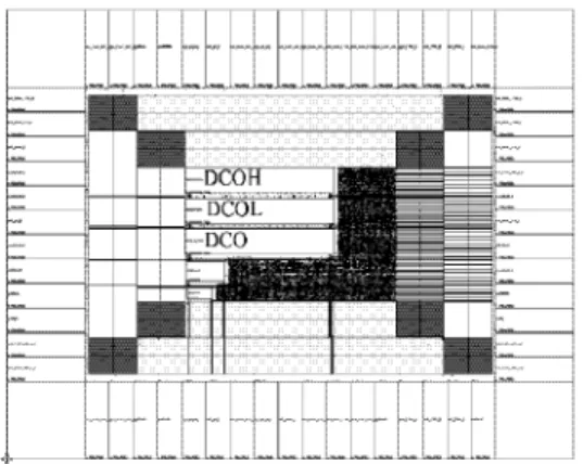
prototype ADPLL design is designed and realized usingUMC 0.18pm 1P6M CMOS technology, as shown in Fig. 3 250
7. For linear acquisition step is desirable in proposed 2
200
frequency-estimation algorithm, a high-linearity DCO l
design [6]
can be cited for purpose. Withpost-layout
0simulations, the contains frequency acquisition
-10
l0
0
steps
and resolution is about 22 ps. The DCOoperates
from 2 50140MHzto 1030 MHz. Three DCOsare
replicas
forFLE. -3 01__IThe ADPLL core area is
520x530
'm . 2 efrfCyP
8 1 (a) 20 fref Cycles (b)Figure
9.(a)
Phaseerrorv.s.referenceclcok cycles.
(b)ADPLL
frequency out v.s reference clock cycles.
_...
V.CONCLUSIONSDCOH The Frequency-Estimation Algorithm for ADPLL and
m= [DC0L . VLSI architecture
are
presented
inthis paper.Compared
toexisting algorithms, proposed algorithm
realizes the fastest lock-in time of twocycles. Also,
a new scalable LD is utilized forrequirements
of differentapplications.
The prototypedesign
isimplemented
in UMC 0.18 CMOS I~
II~
I I I I I I I I I I I IIprocess with standard-celllibrary.
Thechip
operates from 140 to 1030MHz, and the core area is 520x530ptm2.
The fast-lock ADPLL design can be easily transferred and incorporated into system integration due to its digitalFigure
7.Chip layout
of theprototypeADPLL.(where
DCO:feature.
outerDCO, DCOH: inner DCOoperatedatF, DCOL:inner DCOoperatedatFmin,)
Acknowledgment
For example of fast-lock operation is shown in Fig. 8. The authors thank CIC (Chip Implementation Center)
Inthe initial state, reference clock is 15.625 MHz, N is 32, for CAD tool supports and technical discussions. output clock frequency is 500 MHz, and corresponding
control codeFis 50. AsmultiplicationnumberNswitches
to 48; the FLE is activated; desired F should be 16. The References
output frequency turns out to be 750 MHz in two cycles [1] Takamoto Watanabe andShigenoriYamauchi, "AnAll-DigitalPLL
and the acquisition process is exactly verified with for Frequency Multiplication by4 to 1024 With Seven-CycleLock
simulation inFig. 8. Time,"
2003.
IEEE Journa of Solid-StateCircuit,
vol.38,
no.2,
FebruaryFor a practical industrial application, Fig. 9(a) shows [2] C. Chung and C. Lee, "An all-digital phase-locked loop for
high-the phase difference versus reference clock for 200 MHz.. ~~~~~andSystems,speed clock generation,"vol.3, pp.26-29,IEEE International Symposium onMay 2002. Circuits
frequency
output. Thephase
error at therising edge
of an Sytes vo.3 p2-9 a 02frlequenc
3isoutput.0The phasea
erroratg.
taThe
risin e o [3] I. Hwang, S Lee, S. Lee, and S. Kim, "A digitally controlledphase-cycle 3 iS around 0.047 radian in Fig. 9(a). The desired locked loop with fast locking scheme for clock synthesis
outputfrequencyis shown inFig. 9(b). application," IEEE Int. Solid-State Circuits Conf. Dig. Tech.
Papers,Feb.2000,pp. 168-169
FZF [4] T.-Y. Hsu, C.-C. Wang, andC.-Y. Lee, "Design and analysis of R[9: 24 portablehigh-speedclockgenerator,"IEEE Trans.CircuitsSyst. II,
F19:0] vlo.48, pp. 367-375,Apr.2001.
CLg|_ [5] H.-TAhnand D.J.Allstot,"Alow-jitter1.9V CMOS PLLfor
ultra-CLjjj SPARCmicroprocessor applications,"IEEE K. Solid-StateCircuits,
koutliuI
vol.35,
pp.450-454,
May
1999.[6] Chia-Tsun Wu, Wei Wang,I-Chyn Wey, andAn-Yeu(Andy)Wu,
"A Scalable DCO Design for Portable ADPLL Designs," IEEE
Figure8. Simulation offrequency multiplicationswitch. InternationalSymposiumonCircuits and Systems,pp. 5449-5452,
May2005.