A MEMS micromirror fabricated using CMOS post-process
Ying-Chou Cheng
a,∗, Ching-Liang Dai
b, Chi-Yuan Lee
c, Ping-Hei Chen
a, Pei-Zen Chang
daDepartment of Mechanical Engineering, National Taiwan University, Taipei, 106 Taiwan, ROC bDepartment of Mechanical Engineering, National Chung Hsing University, Taichung, 402 Taiwan, ROC
cDepartment of Mechanical Engineering, Yuan Ze University, 320 Taoyuan, Taiwan, ROC dInstitute of Applied Mechanics, National Taiwan University, Taipei, 106 Taiwan, ROC Received 8 June 2004; received in revised form 27 December 2004; accepted 7 February 2005
Available online 17 March 2005
Abstract
This work describes the fabrication of a micromachined micromirror by the conventional 0.35m CMOS process and a simple maskless post-CMOS process. The micromirror contains a rectangular mirror plate and four pairs of serpentine supported beams, is integrated with a 1× 4 demultiplexer and a four-stage charge pump circuits on a chip. Maskless dry and wet etching processes are the only requirement to suspend the structure. The primary limitation in the fabrication of microstructures has been overcome by the development of a hybrid processing technique, which combines both an anisotropic dry etch and an isotropic wet etch step. A highly reliable wet etching step with high selectivity between aluminum and sacrificial oxide is also reported. Experimental results reveal that the micromirror has a tilting angle of around 5◦at operation voltage of 22.5 V and a dynamic response less than 5 ms. The surface properties of the CMOS micromirror, detailed process flows, measurement set-up and the experimental results are also presented in this work.
© 2005 Elsevier B.V. All rights reserved. Keywords: MEMS; CMOS process; CMOS–MEMS
1. Introduction
The conventional CMOS process enables the co-integration on a single chip of mature integrated circuits with some smart mechanical microstructures. Various fabricating technologies, including LIGA, surface micromachining and bulk micromachining, have been proposed to meet particular industrial requirements. However, the specialized processes may not support the on-chip integration of MEMS devices and circuit. Therefore, the developments of a MEMS struc-ture by a commercial CMOS batch fabrication process have attracted much attention[1,2].
The advantages of using a micromachined micromirror are its low sensitivity to polarization and its functioning in a broad band. The development of MEMS-based mirrors for
∗Corresponding author. Present address: Institute of Applied Mechanics
(Lab. 433), National Taiwan University, 1, Sec. 4, Roosevelt Rd., Taipei 10617, Taiwan, ROC. Tel.: +886 2 33665646; fax: +886 2 26608560.
E-mail address: [email protected] (Y.-C. Cheng).
optical applications, including in projection display systems
[3,4], optical scanners[5,6], variable optical attenuators[7–9]
and other specific applications has attracted much interest re-cently[10]. Prior work on micromirror optical switching has demonstrated the feasibility of making surface or bulk mi-cromachined micromirrors for light beams steering or for use in optical interconnect applications, by silicon deep etching or by the use of expensive SOI (silicon-on-insulator) wafers
[11–14]. However, issues raised in the literature include high process complexity, high operation voltage or power con-sumption and process incompatibility with currently used CMOS process.
This work demonstrates a fully CMOS process compatible micromirror, which contains a mirror plate, a 1× 4 demul-tiplexer and a four-stage charge pump circuits. The standard 0.35m CMOS process and a completely CMOS compat-ible post-process procedure are utilized to fabricate the de-vice. The proposed micromirror is electrostatically actuated and is driven by a square-wave with a 20 Hz repetition fre-quency. Experimental results indicate that the micromirror
0924-4247/$ – see front matter © 2005 Elsevier B.V. All rights reserved. doi:10.1016/j.sna.2005.02.009
The device proposed herein is a micromachined
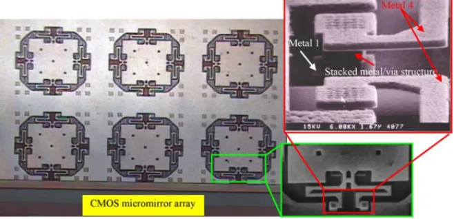
micromir-ror using the conventional CMOS process. A 10× 10
mi-cromirror array with on-chip circuits, as shown inFig. 1, is designed as a testboard for examining the feasibility study of a fully CMOS process compatible micromirror. Therefore, this work investigates the integrating compatibility between stan-dard CMOS process and MEMS devices, the surface quality of mirror plate after post-processing, and the measurement of the dynamic response of a micromirror. However, the to-tal system mentioned previously, a 10× 10 mirror array, is currently under test and development. Possible applications of the MEMS-based micromirrors include the optical atten-uators, precise position sensors, high pixel density display without add-on bonding process or short range data trans-mission.
Electrostatic actuation is used to deflect the micromirror.
Fig. 2(a) depicts the structure and dimensions of a mirror. It contains a top mirror plate with an aluminum layer with a thickness of 1m, four bottom-fixed electrode plates and four pairs of supported beams. The top mirror plate is a movable electrode plate, and four bottom-fixed electrode plates are lo-cated under each side of the mirror plate. The gap between the fixed-electrode plate and mirror plate is about 5.6m. The mirror includes four sets of parallel-plate electrodes, formed from four fixed-electrode plates and the top mirror plate. The supported beams are S-shaped serpentine structures, as indi-cated inFig. 2(b). One end of the supported beams is fixed to an anchor, which is stacked using metal layers and tungsten
Fig. 2. Structure and dimensions of a micromirror structure: (a) mirror plate and fixed bottom electrodes and (b) flexural supported beams.
plugs (vias), and the other end is attached to the top mirror plate. The mirror plate is about 70m × 70 m areas and is about 1m thick. The area of each fixed-electrode plate is 25m × 28 m. The mirror plate and the supported beams used in the CMOS process are all made from metals. All an-chors comprise stacked metal and via layers. The top mirror plate is electrically connected to highly phosphorous-doped
Fig. 3. Stress distribution in a micromirror structure.
(p+ doped) region in the silicon substrate to yield the same electrical potential between mirror plate and p+doped region. For the operation of proposed micromirror, in the unac-tuated state, the mirror plate exhibits no action in relation to the fixed electrode plate, accounting for the fact that the angle between the incident and reflective light beams is almost the same because aluminum is highly optically reflective (>90%)
[15]. No other metal coating add-on process is required in this work, since the mirror plate is made by aluminum and the deposited oxide layer beneath the aluminum is polished by chemical-mechanical-polishing (CMP) in CMOS process. In the actuated state, a voltage is applied to a fixed electrode plate and to the top mirror plate. The mirror plate is pulled down by the electrostatic force, which changes the direction of the reflective light. The micromirror has four operating modes, because of the set-up of four parallel-plate electrode sets.
The electrostatic force, Fs, generated between the plates
by the applied actuating voltage, VDC, can be derived by
con-Fig. 4. Angular displacement vs. applied voltage.
sidering the energy, E, stored between the plates
Fs= ∂E∂d =1 2 ∂C ∂dVDC2 = 1 2 εrε0AV2 DC d2 (1)
where A is the effective area of the plates, d the air gap be-tween the two plates,ε0andεrthe permittivity of free space and the relative permittivity, respectively. Hence, a normal out-of-plane force, Fs, is applied across an air gap, d, between
the fixed electrode plate and the top mirror plate, resulting in a deflection.
The finite element method software, CoventorWare, is uti-lized to simulate the behaviors of the mirror.Fig. 3illustrates the stress distribution of the micromirror in the actuated state. The deformation in the actuated state almost wholly occurs in the S-shaped flexures of the supported beams. The maxi-mum stress, 13 MPa, is below the yield strength of aluminum,
Fig. 6. Simulation of a 1× 4 demultiplexer.
about 90 MPa, and thus the deformation of the micromirror can be operated in elastic range.Fig. 4presents the relation-ship between the applied voltage and the tilting angle of the mirror plate. The maximum tilting angle of the micromirror is about 5◦at a voltage of 22.5 V. The measured tilting angle de-viates from the simulated tilting angle at the applied voltages above 10 V. This deviation is attributed mainly to the slightly softening of the supported beams after ion-bombardment in the reactive ion etching (RIE) processing step or the uncer-tainly in the exact geometry of the micromirror in the foundry process.
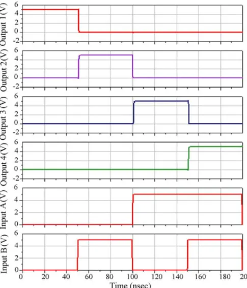
This work uses a simple method to drive the micromirror by a control circuit, as shown inFig. 5. The circuit has a 1× 4 demultiplexer digital circuit and four four-stage charge pump circuits.Fig. 6displays the simulated relationship between the input and output voltage of the 1× 4 demultiplexer. The first four signal curves correspond to the output ports (outputs 1, 2, 3 and 4), which are connected to the four bottom-fixed electrode plates (bottom electrode pads 1, 2, 3 and 4) in the mirror, respectively. The last two signal curves are the input signal. For example, if the input signal is set to A = 1 (high) and B = 0 (low), then the output signal will be sent into output port 2. A voltage signal would be then applied to the bottom-fixed electrode plate (pad 2) to pull down the mirror plate.
3. Device fabrication
The micromachined micromirror is developed accord-ing to the Taiwan Semiconductor Manufacture Company
Fig. 7. Schematic process flow: (a) completion of the CMOS foundry pro-cess, (b) etching silicon dioxide layer by RIE and (c) removing silicon diox-ide layer by BOE/IPA solutions.
(TSMC) CMOS foundry service and design rules. All post-process procedures require only maskless dry and wet etch-ing and thus avoid the sticketch-ing problem. The post-CMOS process has two major steps. The process flow inFig. 7 il-lustrates the development of CMOS compatible micromirror structure in cross-section.Fig. 7(a) describes the schematic cross-sections view after TSMC process. Parts of the passiva-tion nitride on the chip were removed in advance, and the top metal layer was exposed. The oxide layers under the mirror plate and the supported beams are sacrificial layers. Two main steps are involved in the post-CMOS process.Fig. 7(b) illus-trates the use of anisotropic dry etching with CF4/O2to etch
the sacrificial oxide layers. This step removes some of the silicon dioxide beneath the top metal layer and forms some cavities through the etching holes. The suspended structures of the micromirror are not all released. Accordingly, isotropic wet etching of oxide must be performed to release the incom-plete suspended parts, as shown inFig. 7(c). This step was
completed using BOE (six parts 40% NH4F and one part
49% HF) and isopropyl alcohol solution (IPA). Critically, this step enhances the etching selectivity between aluminum and silicon dioxide during wet etching by adding IPA to BOE solution. The suspended structure of the micromirror is re-leased completely, and no sticking occurs after the overall
Fig. 8. The lateral etch-rate test-key of BOE for the silicon dioxide: (a) before test and (b) during test.
post-processing. However, the etch time, 40 min, must be precisely controlled to prevent a short circuit which could be caused by leaving a thin oxide layer to cover the bottom-electrode plates.
Fig. 8 depicts a test-key for detecting the lateral etch-rate of BOE for silicon dioxide. The test-key as shown in
Fig. 8(a) contains five elements with different dimensions: 2m × 2 m, 4 m × 4 m, 6 m × 6 m, 8 m × 8 m
and 10m × 10 m. Each element is composed of the
sil-icon dioxide and the aluminum layer, and the silsil-icon diox-ide layer is under the aluminum layer.Fig. 8(b) illustrates that the silicon dioxide under the aluminum layer generates the lateral etching during the test-key etched by BOE. The lateral etch-rate of BOE for the silicon dioxide can be es-timated in accordance with the required time of each alu-minum layer to be lift-off in the test-key. For example, the lateral etching distance is 1m if the aluminum layer (area of 2m × 2 m) generates lift-off, and recording the etch-time.
Fig. 9reveals the relation between the lateral etch-distance and the etch-time for the silicon dioxide etched by BOE. The lateral etch-rate of BOE for the silicon dioxide evaluated by the experimental results (Fig. 9) was about 8500 ˚A/min. On the other hand, the etch-rate of BOE for the aluminum was in-vestigated by measuring the surface profile of the aluminum
Fig. 9. The lateral etch-distance vs. the etch-time for the silicon dioxide etched by BOE.
Table 1
Experiment parameters of the dry and wet etching steps Etch recipes for the sacrificial oxide
Dry etching BOE/IPA wet etching
CF4+ O2 NH4F (40%) + HF (49%), 6:1
Pressure (mTorr) 10 Steps:
Power (W) 180 (1) Acetone + H2O, 30 min (clean process)
Gas flow (sccm) 16.8CF4+ 4O2 (2) BOE:IPA (9:1), 40 min (etching step)
Temperature (◦C) 25 (3) IPA, 15 min
(4) H2O, 5 s (remove reaction product on the top metal surface)
(5) IPA (or acetone), 15 min (rinse)
(6) Hot bake (120◦C for 20 min)
Etch rate ( ˚A min−1) ∼ 900 ∼8500 (low etch rate but good selectivity)
layer on the chip. First, the thickness of the aluminum layer measured by the surface profile was 2.20m. Then, the alu-minum layer was immersed in BOE with 10, 20 and 30 min, and the thickness of the aluminum layer reduced as 2.18, 2.15 and 2.08m, respectively. The average etch-rate of BOE for the aluminum evaluated by the measurement was about 315 ˚A/min. According to the etch-rate of BOE for the silicon dioxide and the aluminum, the etching selectivity could be expressed as 27:1.
Table 1summarizes the dry and wet etching steps along with the experimental parameters. The ratio of tetrafluo-romethane (CF4) and oxygen (O2) is the decisional recipe
when CF4/O2 RIE are applied to etch silicon dioxide
anisotropically. Combining lower O2flow and low pressure
produces a thin polymer passivating film on the silicon diox-ide sdiox-idewall that inhibits lateral etching. As for the wet etch-ing step in the final procedure, it is well known that one of the most difficult fabrication steps in surface micromachin-ing is the sacrificial etch step and subsequent releasmicromachin-ing of the moveable structures. Especially when aluminum is used as the main structures or the interconnect layers it is diffi-cult to selectively etch the sacrificial oxide without attacking the aluminum. Traditional methods to prevent aluminum at-tack during sacrificial oxide etching are the protection of the metallization using photo-resist (PR) and the use of alterna-tive etch solution like ‘pad-etch’ [16]or HF vapor etching technique. However, these methods have disadvantages: PR protection is only possible when etch time is limited to sev-eral minutes due to adhesion problems. Special etch mixtures or methods can offer reasonable selectivity, but have a low oxide etch rate (pad-etch) and without a standard set-up of the etching process (HF vapor etching technique). In this work, an approach to etch sacrificial oxide with special procedure is proposed, as illustrated inTable 1. Addition of IPA to the BOE is preferred since this makes it possible to maintain a liquid film on the surface of the microstructures when they
Fig. 10. Pictures of the micromirrors after the post-CMOS process.
are taken out of the etching solution. The CMOS–MEMS chip should not be rinse in water for a long time, because water addition to the HF-based solution will result in rapid attack of the surface of aluminum due to the violent chemical
reaction between hydrogen and oxygen ions.Fig. 10shows
some photographs of the micromirror structure following the post-CMOS process by SEM (scanning electron microscope) or optical microscope.
Fig. 12. Schematic optical measurement device (AVID) for the CMOS micromirror device.
beams are made of the top metal layer (metal 4). Many etch-ing holes are also designed in the mirror plate to reduce the etching time during the process.
4. Experimental results
The surface quality of the mirror is also the important de-terminer of the success of various optical applications that requires a reflective type mirror with a surface roughness of better than one-tenth of the wavelength and a larger radius of curvature, to ensure the flatness of the mirror. In this investi-gation, the surface roughness and curvature of the mirror were determined using an instrumental interferometer, the WYKO MHT III system, a non-contact, three-dimensional optical in-terferometric profiler. The root-mean-square (R.M.S.), aver-age roughness (Ra) and radius of curvature (ρ) of the
sur-face were measured at 31.91, 27.80 nm and 58 mm in the X-direction, and 36.31, 30.87 nm and 49 mm in the Y-X-direction, respectively, as shown inFig. 11(a) and (b). These measure-ments reveal that the surface scattering is acceptable for com-monly used reflective-type optical components and verifies the compatibility between the standard IC process and the post-CMOS micromachining technology.
Fig. 12 shows the experimental set-up of the
CMOS–MEMS micromirror. The top mirror plate and bottom-fixed electrode plate of the micromirror are con-nected to the grounded pad and the positive power pad, respectively, of the power supply system. A square-wave with peak voltage of 22.5 V is applied to the mirror by the circuit. The top mirror plate begins actuation around 15 V, as observed under a microscope. The switching dynamics is measured using a commercial laser Doppler vibrometer (LDV) system (AVID). The response time is shown in
Fig. 13(a) and (b). The rise time, corresponding to the recovery state of the micromirror, is about 3 ms and, the fall time, corresponding to the pulled-down state is 4.3 ms. The response time is fast enough for several MEMS micromirror applications.
5. Conclusion
This work presents the design and fabrication of a micro-machined micromirror by a fully compatible CMOS process. Experimentally, in this study we perform maskless etching process and obtain good results, including high selectivity in
whole procedure is simple and compatible with the CMOS process. This investigation not only reduces the developing time, but also minimizes the scale by following the advanc-ing CMOS process. The micromirror proposed herein has a monolithic integration capability with circuits and is poten-tially for future applications in optics or other fields by the advanced VLSI process. For instance, some VLSI foundries have provided the thick top metal layer (2 or 3m) already for mixed signal or RF circuit. That will be a good option to develop CMOS–MEMS devices with better material property and device performance.
Acknowledgements
The authors would like to thank Song-Nan Chen, Yao-Tian Huang, Wei-Feng Chien of the Institute of Applied Mechan-ics, National Taiwan University, Professor Chien-Liu Chang for their valuable advice and assistance in experiment. In ad-dition, we would, finally, like to thank the NSC Northern Re-gion MEMS Research Center, the National Chip Implemen-tation Center and the National Center for High-performance Computing for kindly making their complete research facil-ities available.
References
[1] M. Parameswaran, A.M. Robinson, D.L. Blackburn, M. Gaitan, J. Geist, Micromachined thermal radiation emitter from a commercial CMOS process, IEEE Electron Device Lett. 12 (1991) 57–59. [2] V. Milanovic, M. Ozgur, D.C. DeGroot, J.A. Jargon, M. Gaitan, M.E.
Zaghloul, Characterization of broad-band transmission for coplanar waveguides on CMOS silicon substrates, IEEE Trans. Microw. The-ory Tech. 46 (1998) 632–640.
[3] L.J. Hornbeck, Digital light processing and MEMS: an overview advanced applications of lasers in materials processing, in: Sum-mer Topical Meetings on Broadband Optical Networks/Smart Pix-els/Optical MEMS and their Applications, 1996, pp. 7–8.
[4] D.W. Monk, Digital light processing: a new image technology for the television of the future, Int. Broadcasting Convention (1997) 581–586.
[5] D. Hah, C.A. Choi, C.H. Jun, Y.T. Kim, A self-aligned vertical comb-drive actuator using surface micromachining for scanning micromir-rors, in: Proceedings of the IEEE/LEOS International Conference on Optical MEMS, 2003, pp. 151–152.
[6] N. Konno, M. Tsugai, E. Yoshikawa, T. Usami, R. Fujita, Design op-timization and improved performance on the link beam driven, minia-turized scanning mirror device, in: Proceedings of the IEEE/LEOS International Conference on Optical MEMS, 2000, pp. 11–12.
[7] C.H. Kim, N. Park, Y.K. Kim, Reflective-type variable optical attenu-ator using off-axis misalignment, in: Proceedings of the IEEE/LEOS International Conference on Optical MEMS, 2002, pp. 55–56. [8] M.S. Yang, Y.O. Noh, Y.H. Won, W.Y. Hwang, Very low crosstalk
1× 2 digital optical switch integrated with variable optical attenua-tors, Electron. Lett. 37 (2001) 587–588.
[9] C.R. Giles, V. Aksyuk, B. Barber, R. Ruel, L. Stulz, D. Bishop, A silicon MEMS optical switch attenuator and its use in lightwave subsystems, IEEE J. Quant. Electron. 5 (1999) 18–25.
[10] K.N. Lee, D.S. Shin, Y.S. Lee, Y.K. Kim, Micromirror array for protein microarray fabrication, J. Micromech. Microeng. 13 (2003) 474–481.
[11] L.Y. Lin, E.L. Goldstein, R.W. Tkach, Angular-precision enhance-ment in free-space micromachined optical switches, IEEE Photonics Tech. Lett. 11 (1999) 1253–1255.
[12] H. Toshiyoshi, H. Fujita, Electrostatic microtorsion mirrors for an optical switch matrix, J. Microelectromech. Syst. 5 (1996) 231–237. [13] L. Houlet, P. Helin, T. Bourouina, G. Reyne, E. Diffour-Gergam, H. Fujita, Movable vertical mirror arrays for optical microswitch ma-trixes and their electromagnetic actuation, IEEE J. Quant. Electron. 8 (2002) 58–63.
[14] H. Toshiyoshi, H. Fujita, An electrostatically operated torsion mirror for optical switching device, in: Proceedings of the Eighth Interna-tional Conference on Solid-State Sensors and Actuators, 1995, pp. 297–300.
[15] C. Marxer, C. Thio, M.A. Gretillat, N.F. de Rooij, R. Battig, O. Anthamatten, B. Valk, P. Vogel, Vertical mirrors fabricated by deep reactive ion etching for fiber-optic switching applications, J. Micro-electromech. Syst. 6 (1997) 277–285.
[16] J. Buhler, J. Funk, P. Steiner, P.M. Sarro, H. Baltes, Double pass metallization for CMOS aluminum actuators, Transducers 95 (1996) 360–363.
Biographies
Ying-Chou Cheng received his MS degree from National Cheng-Kung University, Taiwan in 1999 and PhD degree from the Department of
Mechanical Engineering of National Taiwan University, Taiwan in 2004. He is currently a research assistant at the Institute of Applied Mechanics, National Taiwan University with the research interests on IC compatible MEMS and microsensors technologies.
Ching-Liang Dai received the MS degree in the Applied Mechanics from National Taiwan University, Taiwan in 1993, and the PhD degree in the Mechanical Engineering from National Taiwan University in 1997. He is currently an assistant professor at the Department of Mechanical Engi-neering, National Chung Hsing University, Taiwan. His research interests are CMOS–MEMS, integrated microsensors and mechanical properties of thin films.
Chi-Yuan Lee received his MS degree from Tamkang University, Taiwan in 1997 and PhD degree from the Department of Mechanical Engineer-ing of National Taiwan University, Taiwan in 2004. He is currently an assistant professor at the Department of Mechanical Engineering, Yuan Ze University, Taiwan. His research interests are MEMS, acoustic device and microfuel cell.
Ping-Hei Chen was born in Taichung, Taiwan on Augest 31, 1958. He received the BSc degree in Mechanical Engineering from National Tai-wan University in 1980. He then received the MS and PhD degrees from the University of Minnesota in 1984 and 1988, respectively. Since 1988, he had been an Associate Professor in the Department of Mechanical Engineering at National Taiwan University. He was promoted to the full Professor at 1996, then served as the vice-chairman for 2 years, and chair-man for 3 years at Department of Mechanical Engineering in National Taiwan University. His current research interests are MEMS, biochips, di-amond film wafer, nanotechnology, thermal and fluid control in MEMS, and packaging for optical devices and IC.
Pei-Zen Chang was born in Chia-Yi, Taiwan, ROC in 1962. He received the BS degree in Civil Engineering from National Taiwan University, Taipei, Taiwan in 1984, and the PhD degree in Theoretical and Applied Mechanics from Cornell University, Ithaca, NY in 1991. His PhD disser-tation was about the Mechanics of Superconducting Magnetic Bearings. He joined the faculty of Institute of Applied Mechanics, National Taiwan University in 1991 and became a professor in 1999. His current research interests are in the area of micromachined sensors and actuators.