行政院國家科學委員會補助專題研究計畫成果報告
※※※※※※※※※※※※※※※※※※※※※※※※※
※ ※
※ 多邊閘極元件的製作比較與特性的研究
※
※
※
※※※※※※※※※※※※※※※※※※※※※※※※※
計畫類別:■個別型計畫
□整合型計畫
計畫編號:NSC-89-2215-E110-022-
執行期間:民國 89 年 08 月 01 日至民國 90 年 07 月 31 日
計畫主持人:林吉聰 國立中山大學電機系 副教授
共同主持人:
本成果報告包括以下應繳交之附件:
□赴國外出差或研習心得報告一份
□赴大陸地區出差或研習心得報告一份
□出席國際學術會議心得報告及發表之論文各一份
□國際合作研究計畫國外研究報告書一份
執行單位:國立中山大學電機系
中
華
民
國
90 年
10
月
30
日
個別型計畫:多邊閘極元件的製作比較與特性的研究
Fabrication, Evaluation and Characterization of Recessed Multi-Gate SOI MOS Device
計畫編號:NSC-89-2215-E-110-022 執行期限:民國 89 年 08 月 01 日至民國 90 年 07 月 31 日計畫主持人:林吉聰 國立中山大學電機系 副教授
計畫參與人員:黃國胤,張世昌 國立中山大學電機系碩士生
一、中文摘要 我們提出一個具有高轉導及低串接電阻 的三邊凹入式多重閘極 SOI 元件. 此一 SOI 元 件的結構有三個特點: (1) 以平臺式隔離代替傳統 LOCOS 隔離及溝渠 式隔離,可避免鳥嘴效應的發生,同時也 免除了以往矽晶膜中挖溝渠的複雜度與 困難度,大大地簡化了隔離製程。 (2) 結合圓角化(rounded)以及凹入式結構來 減少邊緣效應(edge effect)和降低源極 與汲極的串接電阻。 (3) 三面閘極的結構可以在不降低電路集積 密度,增加有效通道寬度提高元件的電流 驅動力。 從我們實驗結果可得知元件的特性趨勢與 3D 模擬結果是一致的。 此外,根據 3D DAVINCI 模擬以及實驗結 果,三邊凹入式多重閘極有四個特點,而這四 個特點證明了三邊凹入式多重閘極在深次微 米領域中優於相同元件參數的傳統 SOI 元件。 (1) 多重閘極元件比傳統 SOI 元件有較佳的短通道效應與 DIBL 效應(drain induce barrier lowing)的免疫力。 (2) 它有較高的轉導及電流驅動力。 (3) 它的崩潰電壓比傳統 SOI 元件高。 (4) 自熱效應(self-heating effect)不會隨 著電流增益增加而增加,因此三邊凹入式 多重閘極對自熱效應有較佳的免疫力。 這四點優點顯示隨著元件尺寸不斷縮小,三邊 凹入式多重閘極適合於高速度低功率消耗的 應用。 Abstract
In this proposed project﹐ we propose and fabricate a triple recessed multi-gate SOI device that has high transconductance and low series resistance. The SOI device structure has three unique features. First, it uses mesa isolation instead of using conventional LOCOS and trench isolation to avoid the bird’s beak effect in LOCOS isolation and the complexity of digging trench in trench isolation. Second, it combines the rounded and gate recessed structure to reduce the edge effect and to lower the
source/drain parasitic resistance. Third, it has three surfaces of gate structure that can increase the effective channel width of the device to enhance the current drivability of the device without reducing the packing density of the integrated circuit. From our experiment results the trends of device characteristics exhibits good agreement with the 3–D simulation results. According to the simulation results of 3–D DAVINCI and the measurement results, the triple recessed multi-gate SOI MOSFET’s presents four unique characteristics, which are superior to those of conventional SOI with the same device parameter in deep sub-micrometer regime. First, multi-gate SOI has better short channel effect and drain induce barrier lowing immunity than that of conventional SOI device. Second, it has higher transconductance and higher current drive capability. Third, the breakdown voltage is higher than that of conventional SOI device. Fourth, self-heating effect would not increase with current gain. Thus, the triple recessed multi-gate SOI device has better self-heating effect immunity. These four advantages show that the triple recessed multi-gate SOI MOSFET’s is suitable for high speed and low power applications along shrink of device dimensions.
二、計畫緣由及目的
SOI (Silicon-On-Insulator) technology offers superior CMOS devices with higher speed, higher density, and low-power VLSI circuit applications [1] [2]. It offers several advantages over bulk devices as follows.
(1) The parasitic capacitances of SOI MOS devices are smaller than those of bulk ones. (2) SOI CMOS technology has no conventional
latch-up effect and offers a higher
integration density than bulk CMOS.
(3) SOI devices have better immunity against radiation.
(4) SOI MOS devices have lower leakage current and better short channel effect immunity than bulk MOS devices.
(5) In addition, simple process and compatibility CMOS fabrication processes are the reasons for why SOI are popular.
The continuous advancement in ULSI technology and the widespread interest in low power electronics have accelerated the scaling of MOSFET channel lengths into the deep sub-micrometer regime. Along downsizing of MOSFET’s dimensions, the packing density will be increased. However, there are some effects becoming severe, such as short channel effect, narrow channel effect, hot carry effect… etc. Besides, in order to reduce power dissipation in deep sub-micrometer regime, the supply voltage and threshold voltage are also scaled down. In this thesis, we design and fabricate a triple
recessed multi-gate SOI NMOSFET’s
(3RMGSOI) satisfied for above requirements. 三、研究方法與成果
The triple recessed multi-gate SOI
NMOSFET’s structure (3RMGSOI) is shown in Fig.1, only upper, left, and right side gates are performed with thin film. The recessed multi-gate SOI NMOSFET device structure has three unique features.
(1) Mesa isolation technology:
There are three main isolation schemes for SOI devices [3]. The most used methods of isolating active areas on an SOI substrate are the local oxidation of silicon (LOCOS), shallow trench isolation (STI), and mesa isolation processes. LOCOS isolation cannot be easily scaled into the sub-0.25-um regime due to bird’s beak problem and STI isolation needs a lot of development efforts and is an expensive process because that
chemical mechanical polishing and
additional mask are needed. The simplest scheme is the mesa isolation. The mesa isolation can be realized by dry etching on the top silicon film of the SOI substrate. We use mesa isolation to define active region.
(2) Recessed gate str uctur e:
The main advantage of recessed technology is reducing source and drain series resistance [4]. It usually uses LOCOS or reactive ion etching (RIE) to perform the recessed region. We use RIE technology to reduce series resistance on the triple recessed multi-gate SOI MOSFET’s.
(3) Rounded active r egion:
Sidewall edge effect occurs at the edge of the mesa islands, which leads to a smaller threshold voltage and larger leakage current [5]. We use rounded technology, which
combines mesa with LOCOS isolation, to make the edge rounded and eliminate edge effect [6].
We also design three test devices for performance comparison. Fig. 2 presents the ID
-VG characteristics of these four device, where
the silicon film is 100nm, burier oxide is 400nm, gate oxide is 5.5nm, channel length is 0.6um, mask width is 0.8um, and the channel doping is 1x1017 cm-3. We find out that the triple recessed multi-gate device has the largest Ion current
among them. Besides, there is no hump in our devices due to the rounded edge. The leakage current of triple recessed multi-gate is the lowest among them owing to the sidewall edge effect is suppressed. Fig. 3 presents the normalized transconductance of the four devices. We obtain that the triple recessed multi-gate device has the largest normalized transconductance among those devices. Fig. 4 presents the threshold voltage variation being as a function of the mask width, where the channel length is fixed at 0.6um. We obtain that the threshold voltages vary obviously as the mask width scaled down in all multi-gate device. Compared with the multi-gate device, the threshold voltage of conventional SOI shift smoothly as the mask width scaled down. This is due to that the conventional SOI only has single gate and it does not have sidewall-gate coupling effect, hence the threshold voltage shift is not sensitive to mask width. In the multi-gate devices, the
sidewall-gate coupling effect becomes
significant as scaling the mask width, the threshold voltage is much smaller than that of conventional SOI.
Fig. 5 shows the threshold voltage variation as a function of the channel length, where the mask width is fixed at 2.4um. We obtain that the threshold voltage of conventional SOI shifts notably when channel length is scaled down from 0.8um to 0.6um. However, the threshold voltages shift slightly in all multi-gate devices. It demonstrates that the multi-gate devices do have better short channel effect immunity than that of conventional SOI device.
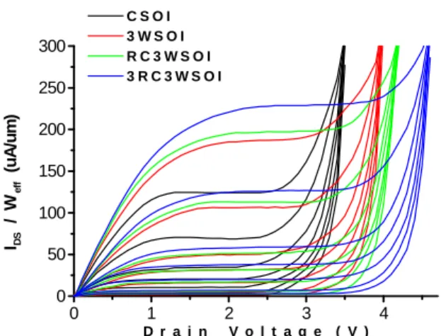
For comparing more easily, we put all the ÎDS
currents in one picture as shown in Fig. 6. First, we obtain that all the multi-gate devices have
higher saturation currents than that of
conventional SOI device and the triple recessed multi-gate device has the highest ÎDS among
them. Second, the breakdown voltages are postponed in multi-gate devices, and the
breakdown voltage of the triple recessed multi-gate is the highest among the four
architectures. Therefore, the multi-gate
architectures have higher current drive
capability and higher breakdown voltage than that of conventional SOI architecture. In the triple recessed multi-gate device, the breakdown is about 50% larger than that of conventional SOI device. In addition, the self-heating effect is
not obvious in our measured ID - VDS
characteristics. We found out that the
self-heating effect in obvious in a CSOI Device as VG- VTH = 2V, whereas the self-heating effect
is slight in the multi-gate device. Fig. 7 presents the excess current gains as a function of VG- VTH
with different mask width for multi-gate devices. First we compare the experiment (black line) with simulation result (blue line), we obtain that the simulation excess current gains are larger than that of experiment. It is due to the large source/drain series resistance of our experiment device. Second we compare the experiment (black line) with experiment (red line) in the same figure. We find out that the excess current gains are larger as the mask width is smaller.
四、結果與討論
We have successfully fabricated triple recessed multi-gate SOI NMOS device in this project. We used recessed technology to raise the source and drain for reducing the source/drain series resistance, and exploited the rounded process to suppress the edge effect. According to the simulation results of 3 – D Davinci and the measurement results, the triple recessed multi-gate SOI device has better short channel effect immunity, lower leakage current, higher current drive capability, and higher breakdown voltage than that of conventional SOI device. Besides, it has excess current gain compared with conventional SOI device and the excess current gain increases with the decrease of effective channel width. The self-heating effect would not increase with current gain, so, the triple recessed multi-gate SOI device has better self-heating effect immunity. Finally, we compare the experiment with simulation results. Although the performance of our experiment is not as good as our expectation, the ID – VG and
ID - VDS characteristics trends shows good
agreement with the simulation results.
Furthermore, we have proposed several
techniques to improve our fabrication process.
五、參考文獻
[1] Yuan Taur and Edward J. Nowak “CMOS Device below 0.1um: How High Will Performance Go?” IEEE Transaction on Electron Devices 1997 P.215-217.
[2] Chenming Hu, “SOI and Device Scaling”. Proceedings 1998 IEEE International SOI Conference, Oct. 1998.
[3] Jong-Wook Lee, Member, IEEE, Hyung-Ki Kim, Woo-Han Lee, Min-Rok Oh, and Yo-Hwan Koh, Member, IEEE, “Hot-Carrier Degradation Behavior of Thin-Film SOI nMOSFET with Isolation Scheme and Buried Oxide Thickness”IEEE Transaction on Electron Devices 2000 P.1013-1017.
[4] Jong-Ho Lee, Hyung-Cheol Shin, Jong-Son Lyu, Bo Woo Kim, and Young-June Park, “ Recessed Channel (RC) SOI NMOSFET ‘s with Self-Aligned Polysilicon Gate Formed on the RC Region” Proceedings 1996 IEEE International SOI Conference, Oct.1996 P.122.
[5] J.B.Kuo “Sidewall-Related Narrow Channel Effect in Mesa-Isolated Fully-Depleted Ultra-Thin SOI NMOS Devices” IEEE Transaction on Electron Devices 1995
P.379-381.
[6] Takahisa Eimori, Toshiyuki Oashi, Fukashi Morishita, Toshiaki Iwamatsu, Yasuo Yamaguchi, Fumihiro Okuda et al, “Approaches to Extra Low Voltage DRAM Operation by SOI-DRAM” IEEE Transaction on
Electron Devices VOL.45, NO.5 MAY 1998
P.1000-1007.
Fig.1 The triple recessed multi-gate SOI NMOSFET’s architecture (3RMGSOI).
Fig. 2 The ID - VG characteristics of the four
devices, where the silicon film is 100nm, burier oxide is 400nm, gate oxide is 5.5nm, channel length is 0.6um, mask width is 0.8um, and the channel doping is 1x1017 cm-3. -0.5 0.0 0.5 1.0 1.5 10-17 10-16 10-15 10-14 10-13 10-12 10-11 10-10 10-9 10-8 10-7 10-6 10-5 10-4 VDS = 0.1V Simulation CSOI Simulation 3WSOI Simulation RC3WSOI Simulation 3RC3WSOI Experiment CSOI Experiment 3WSOI Experiment RC3WSOI Experiment 3RC3WSOI IDS (A) Gate Voltage (V)
-0.5 0.0 0.5 1.0 1.5 0 2 4 6 8 10 12 14 16 18 20 VDS= 0.1V
Exp erim en t CSOI Exp erimen t MGSOI Exp erimen t RMGSOI Exp erim en t 3RMGSOI Simulatio n CSOI Sim ulatio n MGSOI Simulatio n RMGSOI Simulatio n 3RMGSOI g m / W e ff (u S /u m ) Gate Vo lt ag e (V)
Fig. 3 The normalized transconductance, gm/weff,
of the four devices.
Fig. 4 The measured threshold voltage versus the mask width, where the channel length is fixed at 0.6um.
Fig. 5 The measured threshold voltage versus the channel length, where the mask width is fixed at 2.4um.
Fig. 6 Comparison of normalized output characteristics of these four devices with the silicon film is 100nm, burier oxide is 400nm, gate oxide is 5.5nm, channel length is 0.6um, mask width is 0.8um, and the channel doping is 1x1017 cm-3.
Fig. 7. The excess current gains are as a function
of VG – VTH with different mask width for
multi-gate devices. 0.4 0.6 0.8 1.0 1.2 1.4 1.6 1.8 2.0 2.2 2.4 2.6 0.30 0.35 0.40 0.45 0.50 0.55 0.60 0.65 0.70 0.75 0.80 CSOI 3WSOI RC3WSOI 3RC3WSOI T h re s h o ld V o lt a g e (V )
Channel Length (um)
0 1 2 3 4 0 50 100 150 200 250 300 C S O I 3 W S O I R C 3 W S O I 3 R C 3 W S O I IDS / W e ff ( u A /u m) D r a i n V o l t a g e ( V ) 0.0 0.2 0.4 0.6 0.8 1.0 0 50 100 150 200 250 300 350 VDS= 2.0V
Simulation 3WSOI W eff =1.0um (W m=0.8um T SI =0.1um) Simulation RC3WSOI W eff =0.9um (W m=0.8um T SI =0.05um) Simulation 3RC3WSOI W eff =0.8um (W m=0.7um T SI =0.05um) Experiment 3WSOI W eff =1.0um (W m=0.8um T SI =0.1um) Experiment RC3WSOI W eff =0.9um (W m=0.8um T SI =0.05um) Experiment 3RC3WSOI W eff =0.8um (W m=0.7um T SI =0.05um) Experiment 3WSOI W eff =1.8um (W m=1.6um T SI =0.1um) Experiment RC3WSOI W eff =1.7um (W m=1.6um T SI =0.05um) Experiment 3RC3WSOI W eff =1.6um (W m=1.5um T SI =0.05um)
Ge x c e s s (% ) V G - VTH (V) 0.6 0.8 1.0 1.2 1.4 1.6 1.8 2.0 2.2 2.4 2.6 0.30 0.35 0.40 0.45 0.50 0.55 0.60 0.65 0.70 0.75 0.80 CSOI 3WSOI RC3WSOI 3RC3WSOI T h re s h o ld V o lt a g e (V )

![TraditionalMLCalgorithmsmainlytacklethebatchMLCproblem,wheretheinputdataarepresentedinabatch[24,28].Nevertheless,inmanyMLCapplicationssuchase-mailcategorization[22],multi-labelexamplesarriveasastream.Onlineanalysisistherefore dimensionreducermotivatedbyma](data:image/gif;base64,R0lGODlhAQABAIAAAP///wAAACH5BAEAAAAALAAAAAABAAEAAAICRAEAOw==)